
Design of IRIG-B(AC) encoder based on FPGA
2015-03-03 07:51ZHOUCaiqinLIShizhongLIANGGuoqiang
ZHOU Cai-qin, LI Shi-zhong, LIANG Guo-qiang
(College of Mechatronic Engineering, North University of China, Taiyuan 030051, China)
周彩亲, 李世中, 梁国强
(中北大学 机电工程学院, 山西 太原 030051)
Design of IRIG-B(AC) encoder based on FPGA
ZHOU Cai-qin, LI Shi-zhong, LIANG Guo-qiang
(CollegeofMechatronicEngineering,NorthUniversityofChina,Taiyuan030051,China)
InterRange Instrumentation Group (IRIG-B(AC)) code is usually used in the shooting range test for time information transmission and systems time synchronization. According to IRIG-B(AC) code format and modulation principle, this paper presents IRIG-B(AC) coding circuit design scheme based on field programmable gate array (FPGA). The B(AC) code signal is generated by AD7245, a digital-to-analog (D/A) converter. After amplified, the signal can be used directly for system time synchronization, and the amplitude of the signal can be adjusted according to different requirements. The IRIG-B(AC) encoder designed has been verified by test. The test results show that it can output accurate time information and has higher practicality.
IRIG-B(AC) code; field programmable gate array (FPGA); amplitude modulation; time synchronization
0 Introduction
InterRange Instrumentation Group (IRIG) code includes parallel format and serial format. Serial format is used more widely than parallel format because the time code of serial format has far transmission distance. Serial format includes IRIG-A, IRIG-B, IRIG-D, IRIG-E, IRIG-G and IRIG-H, and the difference of them lies in different frame rates. The frame rate of IRIG-B is 1 frame/s, which means that 100 bits pass per second[1]. IRIG-B code has many advantages such as high resolution, large amount of information, and so on.
IRIG-B code can be divided into B(DC) code and B(AC) code. Relative to B(DC) code, B(AC) code has longer transmission distance and higher precision[2]. IRIG-B code based on the international standard has general specification, high reliability and standard interface[3], therefore, it is flexible to be used for range test, communication and other test equipment.
Field programmable gate array (FPGA) has been widely used in industry. IRIG-B(AC) modulation system based on FPGA has high precision, stable performance, small size and low cost[4].
1 IRIG-B(AC) code format and modulation principle
The modulation of B(DC) code to B(AC) code is achieved by means of amplitude modulation of 1 kHz sine signal, as shown in Fig.1.
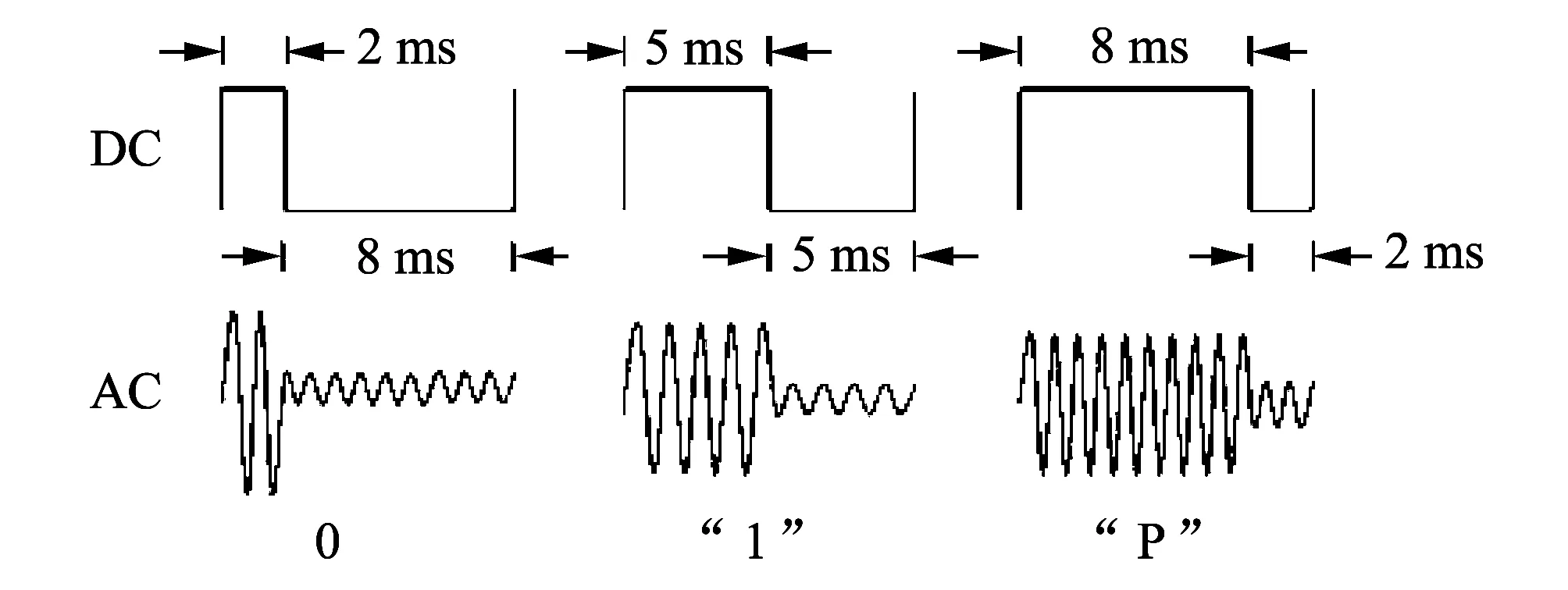
Fig.1 IRIG-B coding
B(DC) code element width has three forms, namely 2, 5 and 8 ms. Different code widths represent different meanings. For B(AC) code, the code element is composed of sine signal at the amplitude ratio of 10∶3. If there are only two high-amplitude sine signals during 10 ms, the code element symbol is “0”; if there are five high-amplitude sine signals, the code element symbol is “1” or index mark; and if there are eight high-amplitude sine signals, the code element symbol is location identification mark “P”[5-6].
A frame period of IRIG-B code contains 100 code elements, and each element width is 10 ms. The pulse rising edge is taken as a time calibraton reference point for code element. The reference mark of the frame consists of a location identification mark and an adjacent reference element. The the code width of PR is 8 ms and it serves as a reference point of a frame[7-8]. IRIG-B code format is shown in Fig.2.
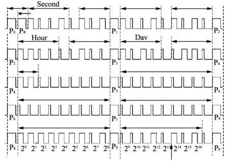
Fig.2 IRIG-B coding format
2 Design of IRIG-B(AC) encoder
The hardware circuit of IRIG-B(AC) encoder is mainly composed of FPGA module, D/A conversion circuit and signal amplification circuit. It is responsible for signal level conversion, output control, encoding of of B code signal. The composition of hardware circuit is shown in Fig.3.
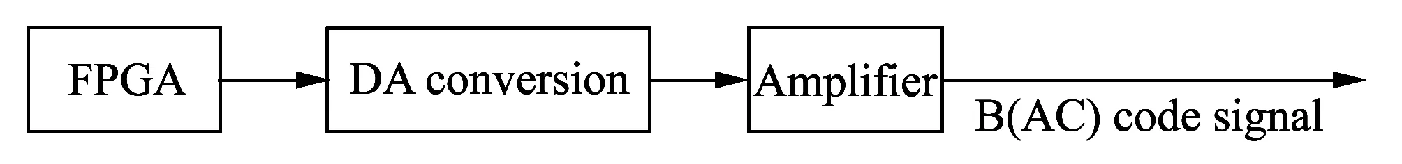
Fig.3 Composition of hardware circuit
2.1 Circuit and coding design of FPGA module
The EP3C16 from Altera is chosen as FPGA chip due to simple hardware circuit, less peripheral devices needed, high integration, high reliability, low power consumption, anti-jamming and high precision. The FPGA module is responsible for real-time encoding for IRIG-B code and controlling the output of IRIG-B(AC) code signal. The hardware connection of FPGA with D/A converter is shown in Fig.4.
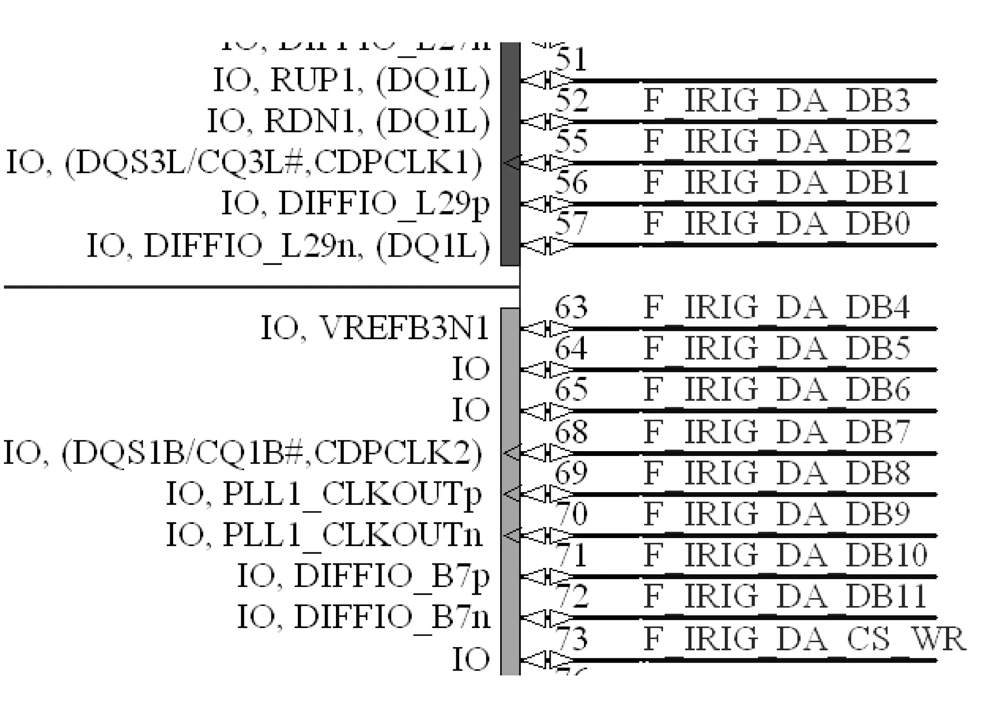
Fig.4 Hardware connection of FPGA with D/A converter
There are many ways to output sine signals by D/A converter under the control of FPGA. Here the look-up table method is selected. The comprehensive program is implemented in Quartus II environment. The ROM IP core is adopted and the sine value table is stored in the ROM.
The 2-port ROM is set up in FPGA chip. The space can store a .mif file, which is a coding table for sine wave output by 12 bit D/A converter. The top 1 000 address space of the coding table holds high-amplitude sine data, and the next 1000 address space of the coding table holds low-amplitude sine data. The two groups of data can produce the signal at the amplitude ratio of 10∶3[9]. The mif file is programmed by Matlab, and main program is shown as follows:
depth=1 000;
width=12;
x=(round(2 047*sin((2*pi*(0∶1 000))/1 000)))+2 048;
y=(round(614*sin((2*pi*(0∶1 000))/1 000)))+2 048;
fid=fopen(‘D:sine1.mif’,‘wt’);
fprintf(fid,‘WIDTH=%d; ’,width);
fprintf(fid,‘DEPTH=%d; ’,depth*2);
fprintf(fid,‘ADDRESS_RADIX=DEC; ’);
fprintf(fid,‘DATA_RADIX=UNS; ’);
fprintf(fid,‘Content Begin ’);
for(k=1∶depth)
fprintf(fid,‘%d:%d ; ’,k-1,x(k));
厅堂石,指天然形成的,石质高雅、色泽细润、造型独特、个体适中、具有较高品位的观赏石。如龙化石、贵州红、晶体石等。
end
for(k=1:depth)
fprintf(fid,‘%d:%d ; ’,k-1+1 000,y(k));
end
fprintf(fid,‘end;’);
fclose(fid).
2.2 Hardware design of D/A module
The output of FPGA is digital signal, and sine signal of B(AC) code is analog signal. Therefore, D/A conversion is needed and 12 bit D/A conversion chip AD7245 is adopted. It has a variety of output voltage ranges and the maximum output voltage is ± 5 V. The range of the output voltage used in the system is from -5 V to + 5 V. The circuit schematic diagram of AD7245 is shown in Fig.5.
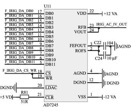
Fig.5 Circuit schematic diagram of AD7245
The amplification circuit consists of OP282, resistors and capacitors. In D/A module, Rx17 can adjust the offset of the output signal, and Rx13 can increase or decrease the output signal voltage in order to meet the different requirements. The signal amplification circuit is shown in Fig.6.
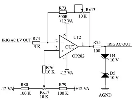
Fig.6 Signal amplification circuit schematic diagram
3 IRIG-B(AC) encoder test
The FPGA is the core controller of the encoder. In order to guarantee high-precision time synchronization, the time sequence of IRIG-B code is generated by FPGA. After IRIG-B is recoded, the D/A synchronous control signal is generated. The working process of the encoder is as follows:
Firstly, FPGA produces the time sequence of IRIG-B code. And then the address of the ROM is searched according to the produced time sequence of IRIG-B code. If the B code is “1” , the address of high-amplitude sine signal will be found; if the B code is “0”, the address of low-amplitude sine signal will be found. According to the ROM address, the sine table is output to data input port of the corresponding D/A converter. Finally, D/A conversion is completed and the sine wave is output according to the control signal D/A. After the converted signal is amplified, the IRIG-B (AC) code can be used directly[12]. The sine wave diagram of the IRIG-B(AC) code is shown in Fig.7.
Considering actual demands, the peak voltage of sine wave with high amplitude is 10 V and the peak voltage of sine wave with low amplitude is 3V, as shown in Fig.8.
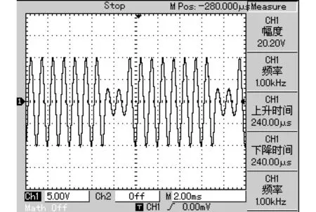
Fig.7 Sine wave diagram of IRIG-B (AC) code
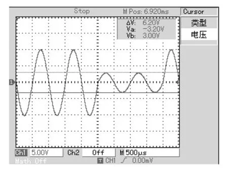
Fig.8 Voltage amplitude of IRIG-B(AC) sine wave
4 Conclusion
The IRIG-B(AC) encoder is designed based on FPGA to complete all logic functions. The modulation of IRIG-B(AC) code is implemented by FPGA and D/A converter. The hardware design of the encoder is simple, and software design is based on modular programming. The designed system has been verified by test. The results show that the performance of the encoder is stable and reliable.
In the test, the encoder outputs serial time code, and the time code is demodulated by standard B code demodulator, thus the correct time information can be got. According to the specific application envir-onments, the initial time value can be set by the used application software. The system has good practical value.
[1] GUO Bin, SHAO Qing-xiao, XIAO Chang-yan, et al. A study of Bei-dou and GPS dual-mode synchronization technology for electric power system clock. Computer Measurement & Control, 2011,19(1):139-141.
[2] LI Jian-wu, QIAO Zheng-sheng, LONG Li-ni.A method of digital modulation of IRIG-B(AC) code. China Water Transport, 2008, 8(9): 121-122.
[3] PANG Ji-yao. Implementation of IRIG-B encoder based on FPGA. Modern Electronics Technique, 2009, 32(24): 113-117.
[4] HAO Shuai, HONG Hai-li, REN Yu-fei. Design of IRIG-B(DC) code encoder and decoder based on FPGA. Foreign Electronic Measurement Technology, 2012, 31(08): 64-67.
[5] LI Liang, LI Jie-ran, ZHANG Ye. IRIG-B (AC) code modulation design based on EPM7160S. Electronic Design Engineering, 2010,18(2): 60-62.
[6] TAN Wei-ze, ZHAN Jian. Design for IRIG-B code encoder with embedded microprocessor. Journal of the Academy of Equipment Command & Technology, 2009,20(4): 82-85.
[7] ZHANG Xiang-rong. Circuit design of the interface card with IRIG - B code format decoding. Microcontroller & Embedded System, 2001, (9): 31-33, 36.
[8] LIU Ming-bo, GENG Wen-jian, HUA An, et al. Design and implement of IRIG-B builder and decoder. Foreign Electronic Measurement Technology, 2010, 29(5): 47-51.
[9] ZHANG Xue-ming, ZHANG Zhen-ya, DAI Ming, et al. Filtering and digital phase compensation of IRIG-B(AC) code in airborne equipment. Optics and Precision Engineering, 2009,17(1): 213-219.
[10] XIE Ren-xiang.The decoding of IRIG-B and the realization of net time service. Chengdu: Sichuan University, 2006: 24-28.
[11] TONG Gang, CUI Ming, CAO Yong-gang, et al. Application of MSP430F149 in IRIG-B code demodulator. Computer Measurement & Control, 2007,15(11): 1597-1601.
[12] TANG Bin, XU Qing-fang, YAO Shan-hua. Design of B code time terminal system based on Bei-dou/GPS dual-mode. Electrical Measurement & Instrumentation, 2013, 50(8): 116-120.
基于FPGA的IRIG-B(AC)编码器设计
IRIG-B(AC)码常用于靶场试验中传递时间信息和同步各系统时间。 根据IRIG-B(AC)码的格式及调制原理, 介绍了基于FPGA的IRIG-B(AC)编码电路的设计。 利用AD7245实现D/A转换转换产生B(AC)码信号, 信号经放大后可直接用于系统时间同步, 而且信号幅度可根据不同的使用需求进行调节。 经测试验证, 本系统输出的时间信息准确无误, 有较高的实用性。
IRIG-B(AC)码; FPGA; 调幅; 时间同步
ZHOU Cai-qin, LI Shi-zhong, LIANG Guo-qiang. Design of IRIG-B(AC) encoder based on FPGA. Journal of Measurement Science and Instrumentation, 2015, 6(3): 291-295. [
周彩亲, 李世中, 梁国强
(中北大学 机电工程学院, 山西 太原 030051)
10.3969/j.issn.1674-8042.2015.03.016]
Received date: 2015-05-22 Foundation items: The 10th Postgraduate Science and Technology Fund of North University of China (No. 20131020)
ZHOU Cai-qin (1245113319@qq.com)
1674-8042(2015)03-0291-05 doi: 10.3969/j.issn.1674-8042.2015.03.016
CLD number: TN99 Document code: A
猜你喜欢
中国机械工程(2022年22期)2022-11-25
中国机械工程(2022年7期)2022-04-20
无机化学学报(2021年7期)2021-07-10
科学导报(2021年91期)2021-01-11
今日农业(2020年15期)2020-12-15
考试与评价·七年级版(2020年2期)2020-10-29
红领巾·萌芽(2020年6期)2020-10-27
中北大学学报(自然科学版)(2019年6期)2019-11-22
今日华人(2019年9期)2019-10-16
中国机械工程(2019年17期)2019-09-19
 Journal of Measurement Science and Instrumentation2015年3期
- Journal of Measurement Science and Instrumentation的其它文章
- Numerical simulation of two-phase flow field in underwater sealing device based on dynamic mesh
- Ballistic impact simulation of Kevlar-129 fiber reinforced composite material
- X-ray image distortion correction based on SVR
- Application of adaptive Kalman filter in rocket impact point estimation
- Analysis of movement laws of fragment and shock wave from a blast fragmentation warhead
- Simulation of small-aperture deep hole drilling based on ABAQUS