
单壁碳纳米管-石墨烯杂化材料的自组装及其电学性能
2015-06-05 14:36PrashantaDhojAdhikariYonghunKoDaesungJungChungYunPark
新型炭材料 2015年4期
Prashanta Dhoj Adhikari, Yong-hun Ko, Daesung Jung, Chung-Yun Park,
单壁碳纳米管-石墨烯杂化材料的自组装及其电学性能
Prashanta Dhoj Adhikari1, Yong-hun Ko1, Daesung Jung2, Chung-Yun Park1,2
(1.InstituteofBasicScience,SungkyunkwanUniversity,Suwon440-746,RepublicofKorea; 2.DepartmentofEnergyScience,SungkyunkwanUniversity,Suwon440-746,RepublicofKorea)
以Si为基底,采用气相沉积法制备出石墨烯(G/Si)薄膜。将含1%APTES的苯溶液与G/Si密封,在115℃下加热2 h,G薄膜上自组装单层APTES膜(SAM-G/Si)。将SAM-G/Si浸渍于酸处理后的单壁碳纳米管氯仿液中,45℃干燥即得到单壁碳纳米管-石墨烯杂化材料(SWCNT-G/Si)。结果表明,具有p-型电学性能的G/Si经表面改性后呈现出n-型性能,电容性能得到提高。
1 Introduction
One-dimensional single-walled carbon nanotubes (SWCNTs)and two-dimensional graphene are nanocarbon materials.Both materials have attracted tremendous attentions for fundamental research and applications in field-emission devices,field-effect transistors,supercapacitors,batteries[1-11],solar cells[12,13]and transparent electrodes[14-16],owing to their extraordinary electrical,mechanical,physical, and structural properties.SWCNTs and graphene have many analogous properties,but there are differences between the two due to structuraldifferences.Several attempts have recently been made to integrate these two novel materials together in order to utilize the merits of both[17-22].
Chemical vapor deposition(CVD)is an important mean to synthesis carbon nanomaterials[13,23,24]. To realize the merits of a combined 2D graphene and 1D CNT material,there have been many recent attempts to prepare graphene sheet-CNT hybrid materials.Recently,the fabrication of G/CNT hybrids through CVD is more attractive because it is possible to form covalent C-C bonding between graphene and CNTs,and to prepare G-CNT hybrids with various structures[25-28].However,the as-grown CNTs are usually multi-walled CNTs(MWCNTs).This results in low specific surface areas(SSA)of as-fabricated G-CNT hybrids,and hinders their performance in the area where a high SSA is required,such as energystorage devices.The direct growth of CNTs on graphene oxide(GO)and reduced GO is simple and effective way to obtain G-CNT hybrids with strong graphene-CNT bonding and anticipated nanostructures. But,as-grown CNTs were still MWCNTs with a poor graphitization due to the high solubility of catalyst nanoparticles in GO or reduced GO[29].Besides,the high defect density of GO or reduced GO also limits the quality of graphene in as-fabricated G-CNT hybrids,and thus hinders their performance.Compared with MWCNTs,the SWCNTs have much large surface area and low defectdensity.Recently,Ning and co-workers demonstrated a one-step synthesis of GSWCNT hybrids by CVD with a mixed catalyst of MgO and Fe/MgO,in which MgO served as the template for the deposition of graphene and Fe/MgO served as the catalyst for the growth of SWCNTs,as well as the graphene layers[30].Nevertheless,to prepare purely SWCNT-graphene hybrid in this technique is difficult due to the poor stability of the catalyst nanoparticles on metal surface.
In order to improve the quality of SWCNT-graphene hybrid that is well interconnected and has superior durability/applicability features for use in device fabrication,we report a simple approach first time to prepare the SWCNT-G hybrid,in which functionalized SWCNTs were chemisorbed onto the supported graphene film that was immobilized with a monolayer self-assembled from 3-aminopropyltriethoxysilane (APTES).This method could be useful as a new route to the fabrication of graphene hybrid materials for various potential applications.
2 Experimental
2.1Reagents and materials
Isopropyl alcohol(IPA),3-aminopropyltriethoxysilane(APTES),toluene,SWCNTs,chloroform,nitric acid and membrane filter paper were purchased as received.Deionized water was used throughoutthe whole experiment.
2.2Graphene synthesis
Graphene was synthesized on copper foil by CVD method.Briefly,Cu foil was pre-annealing up-to 1 050℃in a reactor for 30 min under Ar. Then,methane was introduced into the reactor for 30 min,followed by a cooling down under Ar flow. The graphene grown via CVD was transferred onto a silicon substrate(SiO2/Si)by copper etching technique(G/Si)[31].
2.3Fabrication of self-assembled monolayer onto graphene surface
The graphene on the silicon substrate was irradiated by UV light for 30 min.Then,a glass beaker containing 1%APTES in toluene and UV-treated G/Si were placed in an air-tight steel box.The box was loaded into a processing chamber and heated up to 115℃for 2 h.An APTES was self-assembled to form a monolayer on graphene.Finally,as-fabricated self-assembled monolayer(SAMs)on graphene was rinsed with toluene and ethanol,and then dried by under a N2stream to obtain SAM-G/Si[32].
2.4Functionalization of SWCNTs
25 mg of SWCNTs and 50 mL of HNO3were mixed and refluxed overnight and later the mixtures were vacuum distilled,washed several times with water and dried in vacuum oven at 60℃for 1 h.
2.5Loading of SWCNTs onto graphene surface
The surface functionalized SWCNTs were dispersed in chloroform by ultrasonication for 3 h and then,SAM-G/Si substrate was dipped into solution overnight at 45℃.The SWCNT-loaded graphene on substrate was washed by ethanol and dried by blowing N2gas to obtain SWCNT-G/Si.
2.6Characterization
The surface modified substrates were characterized by Raman spectroscopy.Raman spectra were obtained using a Renishaw,1 000 micro-Raman spectrometer at an excitation wavelength of 514 nm, where at leastthree different sites were sampled.The substrates were further evaluated by X-ray photo electron spectroscopy(XPS).XPS spectra were obtained using a theta probe(VGMICROTEC,ESCA 2000) with a monochromatic Al Kαsource at a pressure of 2×10⁻⁹mbar.The surface morphology of samples was characterized using a field emission scanning electron microscope(FE-SEM,JEOL,JSM-7500F) at an accelerating voltage of 15 kV.The electrical properties of the SWCNT-G hybrid were examined using a 4200-scs Keithley semiconductor analyzer. Electrochemical characterizations of G/Si and SWCNT-G/Si were performed by cyclic voltammetry analysis in a three-electrode half shell system in 1 mol/L H2SO4solution.
3 Results and discussion
The acid-treated SWCNTs were evaluated by Raman spectroscopy.The radial breathing mode peak (RBM),G and 2 D peaks are seen at182,1 587 and 2 679 cm-1respectively for pristine SWCNTs as shown in Fig.1 a.However,after the acid treatment those peaks were not changed substantially,but a D peak clearly appears at 1 350 cm-1,indicating that surface defects are generated in SWCNTs by an acid oxidation(Fig.1b).The surface-functionalizedSWCNTs were further evaluated by XPS.Pristine SWCNTs sample is shown to have an overall oxygen content of 4%as shown in Fig.1c,but after the acid oxidation,the oxygen content is increased to 17% (Fig.1d),indicating that the surface treatment leads to a formation of sufficient surface functionalized groups(—OH,—COOH)in SWCNTs as expected, which might be helpful for their binding onto functionalized CVD-grown graphene film.The non-aqueous dispersion of SWCNTs into solvent is found more effective for acid treated ones rather than pristine SWCNTs,which could be also due to the introduction of hydrophilic groups into SWCNTs surface as shown in Fig.2(Inset).In addition,fabrication of SAMs onto graphene surface was evaluated by XPS and itis found that there is no evidence of formation of N peak for pristine graphene(Fig.3a)but for the SAMs fabricated sample a well-constructed N peak appears, confirming that abundant amine-terminated group is liberated onto graphene surface as shown in Fig.3. Compared with the graphene without the UV treatment(Fig.3b),the UV-treated one has a high N content of(Fig.3c),which is four times as that of the un-treated one,indicating that amine group is sufficiently loaded onto graphene surface as shown in Fig.3c[33].This indicates that the UV-treated sample liberates sufficient oxidize molecules onto graphene surface that is favorable for fabricating SAMs.
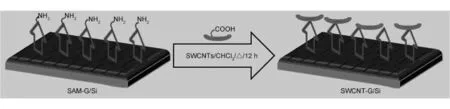
Fig.1 Schematic illustration of SWCNTs covalently linked onto graphene surface.
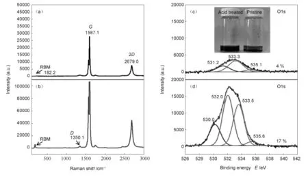
Fig.2 Raman and XPS spectra of SWCNTs before and after acid treatment: (a,b)Raman spectra of(a)pristine SWCNTs and(b)SWCNTs treated by oxidized acid;(c,d)XPS spectra of(c)SWCNTs and (d)SWCNTs treated by oxidized acid(Inset:the photographs of the dispersions of acid-treated SWCNTs and pristine SWCNTs).
In order to further examine whether the SWCNTs are electronically coupled with graphene surface or merely physically attached,Raman bands of pristine and the acid-treated SWCNTs onto SAM-G samples are compared.The acid-treated SWCNTs are chemisorbed onto SAM-G,causing a change of the G and 2 D bands and also RBM peak position.However, there is no change of bands in SAM-G surface for thepristine SWCNTs onto SAM-G,indicating that there is no chemical interaction between SWCNTs and graphene surface.
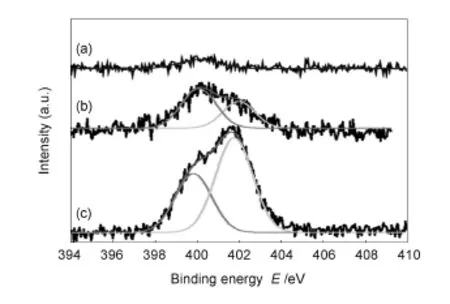
Fig.3 N1s XPS spectra for(a)G/Si,(b)SAM-G/Si without out UV treatment and(c)with UV treatment.
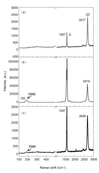
Fig.4 Raman spectra for(a)SAM-G,(b)acid treated SWCNTs and(c)SWCNT-G/Si.
Morphologies of SWCNTs,G/Si and SWCNTG/Si were evaluated by SEM as shown in Fig.5. After the acid-treated SWCNTs are chemisorbed onto graphene surface,they are commonly communicated with graphene as shown in Fig.5 c,consistent with the Raman results.
To further confirm the chemical bonding,the acid-treated SWCNTs sorbed onto garphene surface was evaluated by XPS as shown in Fig.6.The N1s peak of SAM-G/Si is observed in the range of B.E. 399-402 eV.But,after the acid-treated SWCNTs are sorbed onto graphene surface the N1s peak is clearly divided and splitting peak is seen at higher B.E.~405 eV,which should be originated by amide bond. This result confirms the sorption of SWCNTs onto graphene surface is of chemicalnature[31,34].To evaluate their electrical characteristics induced by chemisorption between the SWCNTs and functionalized graphene,field-effect transistors measurements(FET) were carried out as shown in Fig.7.Pristine,functionalized and hybrid graphene FET were fabricated on SiO2/Si substrates using platinum for the source and drain electrodes and 1-butyl-3-methylimidazolium (BmimPF6)as an ionic liquid.The schematic procedure of FET measurements is shown in Fig.7 (Inset).The charge neutrality point for G/Si without surface treatment is near to positive site of zero volt (Fig.7a)but for the UV-treated G/Si,it is further shifted to the same positive site,indicating a p-type doping,which could be resulted from the-COOH, OH group via UV-treatment(Fig.7b).However, after SAMs fabrication on the UV-treated G/Si the charge neutrality point is shifted to negative site of zero volt,meaning a n-doping into graphene surface due to amine terminated SAMs deposition onto graphene surface(Fig.7c).But,after the acid-treated SWCNTs are chemisorbed onto SAM-G/Si,the n-type characteristic is reduced,indicating that doping of p-type material,which could be contributed from the SWCNTs(Fig.7d).Based on these results,itis expected that lone pair of electron from amine in SAMs may donate electron onto graphene,thereby, increasing the charge carrier concentration and therefore increasing the conductivity of SAM-G/Si sample.However,the chemisorption of SWCNTs onto its surface leads to a reduction in the resistance and reaches conductivity beyond position(Figure was not shown).This observation strongly suggests that the exceedingly conductive SWCNTs bonded with graphene[35].Therefore,stable binding of SWCNTs onto graphene surface in present work could be very applicable in storage devices.
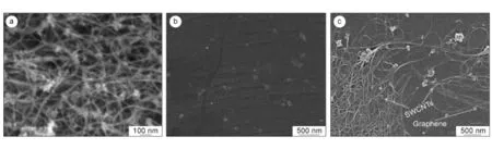
Fig.5 SEM images of pristine(a)SWCNTs,(b)G/Si and(c)SWCNT-G/Si.
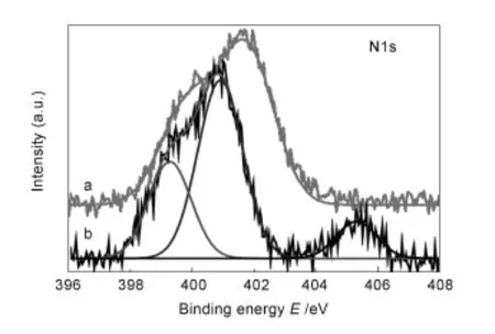
Fig.6 XPS N1s spectra of(a)SAM-G and(b)SWCNT-G/Si.
Moreover,the electrochemical properties of pristine and the hybrid materials were studied using them as working electrodes and 1 mol/L H2SO4for electrolyte solution at a scan rate 20 mV/s.Fig.8c and 8 d show the typical charge/discharge curves of the G/Si and SWCNT-G/Sisamples.The linear and symmetrical curves are indicative of the excellent electrochemical stability and charge/discharge properties as shown in Fig.8.The capacitance from the discharge curves is calculated using the following equation C=i×Δt/ ΔV[36].Where,i is the discharge current density (0.1 mA·cm-2),Δt is the duration of the discharge from+0.8 to-0.8 V(ΔV).
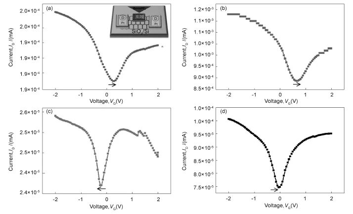
Fig.7 I-V measurement for(a)G/Si, (b)UV-treated G/Si,(c)SAMs/Si and(d)SWCNT-G/Si(Inset:schematic representation of FET device).
The discharge time for the SWCNT-G/Si is slightly greater than the G/Si sample and specific capacitance for the hybrid and pristine samples are calculated to be 6.01 and 5.03 mF/cm2respectively,indicating that the SWCNT-G/Si offers the larger charge capacity than the G/Si.Based upon the peak positions of Fig.8,the possible reason of the present result is that the SWCNT fibrils promote the electron transfer between SWCNTs and graphene electrode.In addition,the immobilization of SWCNTs creates the larger surface area onto the hybrid graphene electrode.Therefore,the surface functionalization of SWCNTs and graphene is found more effective to integrate them into the SWCNT-G hybrid,which could be implemented to fabricate supercapacitor.The present simple technique might be utilized to prepare other nanomaterials too.
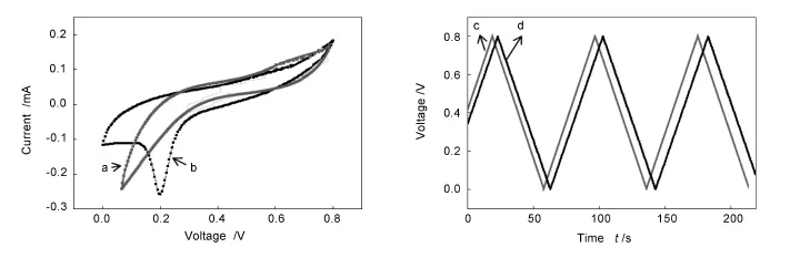
Fig.8 Cyclic voltammogram curves of(a)pristine graphene and(b)SWCNT-G at a scan rate of 20 mV/s in 1 mol/L H2SO4solution. (c,d)Their galvanostatic charge/discharge curves respectively.Supercapacitor performance of hybrid film showing high specific capacitance owing to a large surface area and marginally higher electrical conductivity.
4 Conclusions
We have developed a simple method to integrate SWCNTs onto CVD grown graphene film via immobilization technique.The amine groups on graphene promote the chemisorption of the acid-treated SWCNTs.A p-type characteristic of the G/Siis shifted to n-type electrical properties after immobilized with SAMs of APTES and hybridized with SWCNTs, which improves the specific capacitance.This approach could be of great use in the fabrication of supercapaicitors,flexible hybrid electrodes and other future applications.
Acknowledgements
This research was supported by Basic Science Research Program through the National Research Foundation of Korea(NRF)funded by the Ministry of Education(2009-0094023).
[1] Novoselov K S,Geim A K,Morozov S V,et al.Electric field effect in atomically thin carbon films[J].Science,2004,306: 666-669.
[2] Liang J,Xu Y,Huang Y,et al.Infrared-triggered actuators from graphene-based nanocomposites[J].J Phys Chem C, 2009,113:9921-9927.
[3] Wang X,Zhi L J,Mullen K.Transparent,conductive graphene electrodes for dye-sensitized solar cells[J].Nano Lett,2008,8: 323-327.
[4] Yoo E,Kim J,Hosono E,et al.Large reversible Li storage of graphenenanosheet families for use in rechargeable lithium ion batteries[J].Nano Lett,2008,8:2277-2282.
[5] Schwierz F.Graphene transistors[J].Nat Nanotechnol,2010, 5:487-496.
[6] Stoller M D,Park S,Zhu Y W,et al.Graphene-based ultracapacitors[J].Nano Lett,2008,8:3498-3502.
[7] Simon P,Gogotsi Y.Materials for electrochemical capacitors[J]. Nat Mater,2008,7:845-854.
[8] Dong X C,Shi Y M,Huang W,et al.Electrical detection of DNA hybridization with single-base specificity using transistors based on CVD-grown graphene sheets[J].Adv Mater,2010, 22:1649-1653.
[9] Huang Y X,Sudibya H G,Fu D L,et al.Label-free detection of ATP release from living astrocytes with high temporal resolution using carbon nanotube network[J].Biosensor Bioelectron, 2009,24:2716-2720.
[10] Huang Y X,Dong X C,Shi Y M,et al.Nanoelectronic biosensors based on CVD grown graphene[J].Nanoscale,2010, 2:1485-1488.
[11] Dong X C,Fu D L,Xu Y P,etal.Label-free electronic detection of DNA using simple double walled carbon nanotube resistors[J].J Phys Chem C,2008,112:9891-9895.
[12] Jia Y,Cao A,Bai X,et al.Achieving high efficiency siliconcarbon nanotube heterojunction solar cells by acid doping[J]. Nano Lett,2011,11:1901-1905.
[13] Arco L G D,Zhang Y,Schlenker C W,et al.Continuous, highly flexible,and transparent graphene films by chemical vapor deposition for organic photovoltaics[J].ACS Nano,2010, 4:2865-2873.
[14] Bae S,Kim H,Lee Y,et al.Roll-to-rollproduction of30-inch graphenefilms for transparent electrodes[J].Nat Nanotechnol, 2010,5:574-578.
[15] Hu L B,Gruner G,Li D,et al.Patternabletransparent carbon nanotube films for electrochromicdevices[J].J Appl Phys,2007,101:016102.
[16] Tantang H,Ong J Y,Loh C L,et al.Using oxidation to increase the electrical conductivity of carbon nanotube electrodes [J].Carbon,2009,47:1867-1870.
[17] Dong X C,Li B,Wei A,et al.One-step growth of graphenecarbon nanotube hybrid materials by chemical vapor deposition [J].Carbon,2011,49:2944-2949.
[18] Li CY,Li Z,Zhu H W,et al.Graphenenano-‘‘patch’’on a carbon nanotube network for highly transparent/conductive thin film applications[J].J Phys Chem C,2010,114:14008-14012.
[19] King P J,Khan U,Lotya M,et al.Improvement oftransparent conducting nanotube films by addition of smallquantities of graphene[J].ACS Nano,2010,4:4238-4246.
[20] Hong T K,Lee D W,Choi HJ,et al.Transparent,flexible conducting hybrid multilayer thin films of multiwalled carbon nanotubes with graphenenanosheets[J].ACS Nano,2010,4:3861-3868.
[21] Fan Z J,Yan J,Zhi L J,et al.A three-dimensional carbon nanotube/graphene sandwich and its application as electrode in supercapacitor[J].Adv Mater,2010,22:3723-3728.
[22] Tung V,Chen L M,Allen M J,et al.Low-temperature solution processing of graphene-carbon nanotube hybrid materials for high-performance transparent conductors[J].Nano Lett,2009, 9:1949-1955.
[23] Adhikari P D,Kim S,Lee S,et al.Immobilization of iron nanoclustures on functionalized silicon substrate and their catalytic behavior to synthesize multi-walled carbon nano tubes[J]. Nanosci and Nanotech,2013,13:4587.
[24] Adhikari P D,Song W,Cha M J,et al.Synthesis of high quality single-walled carbon nanotubes via catalytic layer reinforced by self-assembled monolayer[J].Thin Solid Films, 2013,545:50-55.
[25] Chen S,Chen P,Wang Y.Carbon nanotubes grown in situ on graphenenanosheets as superior anodes for Li-ion batteries[J]. Nanoscale,2011,3(10):4323-4329.
[26] Paul R K,Ghazinejad M,Penchev M,etal.Synthesis of a pillared graphene nanostructure:acounterpart of three-dimensional carbon architectures[J].Small,2010,6(20):2309-2313.
[27] Lv R T,Cui T X,Jun M S,et al.Open ended,N-doped carbon nanotube-graphene hybrid nanostructures as high-performance catalyst support[J].Adv Funct Mater,2011,21(5): 999-1006.
[28] Yu K H,Lu G H,Bo Z,et al.Carbon nanotube with chemically bonded graphene leaves for electronic and optoelectronic applications[J].J Phys Chem Lett,2011,2(13):1556-1562.
[29] Rinaldi A,Tessonnier J P,Schuster M E,et al.Dissolved carbon controls the initial stages of nanocarbon growth[J].Angew Chem Int Ed,2011,50(14):3313-3317.
[30] Zhu X,Ning G,Fan Z,et al.One-step synthesis of a graphene-carbon nanotube hybrid decorated by magnetic nanoparticles[J].Carbon,2012,50(8):2764-2771.
[31] Adhikari P D,Jeon S,Chha M,et al.Immobilization of carbon nanotubes on functionalized graphene film grown by chemical vapor deposition and characterization of the hybrid material [J].Sci and Technol of Adv Mater,2014,15:015007.
[32] Adhikari P D,Tai Y,Ujihara M,et al.Surface functionalization of carbon micro coils and their selective immobilization on surface-modified silicon substrates[J].J Nanosci and Nanotech,2010,10:833-839.
[33] Adhikari P D,Imae T,Motojima S.Selective immobilization of carbon micro coils on patterned substrates and their electrochemical behavior on ITO substrate[J].Chem Eng J,2011,174: 693.
[34] AdhikariP D,Chho J,Park C Y.Easy synthesis of nitrogen doped single-walled carbon nanotubes via using supporting layer as a precursor[J].Material Focus,2014,3:281-285.
[35] Mou Z,Chen X,Du Y,etal.Forming mechanism of nitrogen doped graphene prepared by thermal solid-state reaction of graphite of oxide and urea[J].Appl Surf Sci,2011,258: 1704-1710.
[36] Song R K,Park J H,Sivakkumar S R,et al.Supercapacitive properties of polyaniline/Nafion/hydrous RuO2composite electrodes[J].Journal of Power Sources,2007,166:297-301.
Single-wall carbon nanotube hybridized graphene films: self assembly and electrical properties
Prashanta Dhoj Adhikari1, Yong-hun Ko1, Daesung Jung2, Chung-Yun Park1,2
(1.InstituteofBasicScience,SungkyunkwanUniversity,Suwon440-746,RepublicofKorea;2.DepartmentofEnergyScience,SungkyunkwanUniversity,Suwon440-746,RepublicofKorea)
A SWCNT-G/Si hybrid film was fabricated from graphene(G)film by chemical vapor deposition and single-walled carbon nanotubes(SWCNTs)by an immobilization method,in which a 3-aminopropyltriethoxysilane monolayer was formed on a UV irradiated graphene film by self-assembly,and acid-oxidized SWCNTs were chemisorbed on it.The G/Si,3-aminopropyltriethoxysilane immobilized G/Si and SWCNT-G/Si hybrid films were characterized by SEM,Raman spectroscopy,XPS,and conductivity and electrochemical tests.Results indicate that the immobilization changes the p-type G/Si into n-type by electron donation from a lone electron pair on the amine and the chemisorption reduces the n-type behavior.The SWCNT-G/Si hybrid film has a higher specific capacitance than the G/Si film.This approach could be of great use in the fabrication of supercapacitors,flexible hybrid electrodes and other devices.
Chung-Yun Park.E-mail:cypark@skku.edu
TB332
A
Chung-Yun Park.E-mail:cypark@skku.edu
Prashanta Dhoj Adhikari.E-mail:dhoj2@yahoo.com
1007-8827(2015)04-0342-07
Received date:2015-03-10;Revised date:2015-08-05
Author introduction:Prashanta Dhoj Adhikari.E-mail:dhoj2@yahoo.com
English edition available online ScienceDirect(http://www.sciencedirect.com/science/journal/18725805).
10.1016/S1872-5805(15)60193-7
猜你喜欢
河北果树(2022年1期)2022-02-16
中学生数理化·中考版(2020年11期)2020-12-14
华北农学报(2020年5期)2020-11-10
中学生数理化(高中版.高考理化)(2020年2期)2020-04-21
天然气工业(2019年10期)2019-11-12
心电与循环(2016年6期)2016-12-24
浙江大学学报(工学版)(2016年9期)2016-06-05
中学生数理化·高二版(2016年6期)2016-05-14
原子与分子物理学报(2015年3期)2015-11-24
中国塑料(2014年9期)2014-10-17
