碳纳米管脉冲式场发射中所存在的尖峰及其解决方法
2016-03-22 06:55刘春毅何艳康周公羽
电子器件 2016年1期
刘春毅,何艳康,周公羽,雷 威
(东南大学电子科学与工程学院,南京210096)
碳纳米管脉冲式场发射中所存在的尖峰及其解决方法
刘春毅,何艳康,周公羽,雷威*
(东南大学电子科学与工程学院,南京210096)
摘要:从电路负载方面考虑,将二级平板式碳纳米管场发射结构看做一个电容和可变电阻的并联结构。根据测试数据计算出电容值在皮法级,可变电阻在兆欧到千欧变化。通过电路仿真,分析了此结构在脉冲式下的负载特性。以此得出在脉冲前沿和后沿产生尖峰的原因。根据仿真结构提出增加RLC和二极管来消除尖峰的方法。实验证明,整体负载特性的改变使得发生发射结构上的脉冲尖峰基本得到消除。
关键词:纳米材料;场发射;电路仿真;尖峰消除
Many methods have been proposed to improve the filed-emission characteristic of CNTs in recent years[1-5]. Because the emission current flowing through the CNTs produces heating,it is unstable to get a high filed-emission current in a direct-current driving mode while the CNTs wear under such condition[6]. There⁃fore,the pulsed field-emission operation of a CNT cath⁃ode was introduced.
Lysenkov and Müller[7]investigated the pulsed filed-emission options of a CNT cathode with 80-Hz repetition rate. The peak current density is 60 mA/cm2. Kim et al.[8]measured the pulsed field-emis⁃sion performance of a CNT triode,and a pulsed cath⁃ode current of 2.8 mA is obtained.
In the process of investigating the impulse re⁃sponse of filed-emission diode by experiment,because the field- emission current Iais difficult to be me⁃asured directly,we measure the waveform of current Ieby an oscilloscope(Agilent 54624).
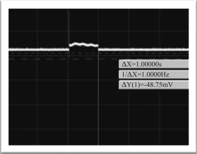
Fig.1 Waveform of current Iemeasured by the oscilloscope(Agilent 54624)
1 Qualitative Explanation
The electronic-circuit model of a CNT diode with a pulse driving mode is shown in Fig.2.
1.1Plate Capacitor of Field Emission Tube
The structure of the CNTs field emission tube in⁃dicates that there is a plate capacitor at load. Since the drive signal to stimulate the CNTs is set as a high volt⁃age pulse signal,the oscillatory frequency at the rising or falling edge of the driving source can be tremendous high(because of the steep slope of both edges). By us⁃ing the theoretical capacitive reactance calculating equation(XC=1/(ωC)),we can estimate the capacitive reactance theoretically. It may be significant small as the frequency ω is high at the edge. In that case,when the drive signal is rising or falling,the capacitor can be regard as short circuited comparing with the measuring resistance,and the whole voltage will be loading on the measuring resistance(Re).Therefore,the waveform on the oscilloscope will show us a sharp peak,up to source voltage.
1.2Parasitic Inductance of Measuring Resistance
Because the measuring resistance has an instinct small parasitic inductance,when we monitor the field emission current,there’s possibility that the inductor,though very small,may contribute to the sharp peak at the rising and falling edges of the waveform.Because the frequency is high when the voltage is rising and falling,the inductive reactance might be pretty high by calculat⁃ing it with the inductive reactance equation(XL=ωL).
Since the source has an internal resistance(up to 10 kΩ)and the voltage will be distributed to the source resistance and the measuring one,when the measuring resistance is much smaller comparing with the source resistance,the voltage loading on the measuring resis⁃tance will be small at the rising and falling edges,with⁃out a distinct sharp peak. Therefore,when considering the source internal resistance,we can make out that the parasitic inductance of the measuring resistance al⁃so makes great contributions to the sharp peak at rising and falling edges.
1.3Primitive Peak of High Voltage Pulse
Since our group using the semiconductor IGBT to shape the pulse signal,there will always exist a natural peak at the rising and falling edges. Because we cannot efficiently eliminate the natural peak and the peak is much small than the observing one,we can take it as a secondary influence of the cutting peak.
1.4 Inner Structure of Oscilloscope
When analyzing the sharp peak,we cannot ignore the hidden influence from the observing oscilloscope. Because the internal circuit of the oscilloscope also contributes to the waveform,we cannot underestimate the possible factors that affect the waveform. For in⁃stance,because the sampling rate determines the sam⁃pling amount in a certain period,the waveforms might be different under different sampling rates,even though the observing voltage remains unchanged.
If the sampling rate is much smaller than the peri⁃od of the sharp peak(several μs),the waveform is cred⁃ible because it’s able to detect such peak. On the oth⁃er hand,if it’s longer than the period of the sharp peak,the waveform may be suspicious because oscillo⁃scope may compose the waveform by continuing the tendency of the rising or falling edge,resulting in a measuring cutting peak while the actual observing volt⁃age is smooth.
In our experiment,we select the appropriate sam⁃pling rate and storage depth to avoid such problem.
2 Theoretical Explanation
In order to explain the main reasons precisely,we have tried to make some theoretical explanations and attain some simulating results:
2.1Field Emission Tube’s Plate Capacitor
To merely analyze the influence from the capacitor,we idealize the electronic-circuit model as the Fig.3. In Fig.3,RBeamis simplified as a constant resistance in or⁃der to facilitate the simulation and experiment.
According to the electronic-circuit model,the fol⁃ lowing equations can be obtained:
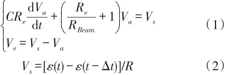
The solution to the equations is:

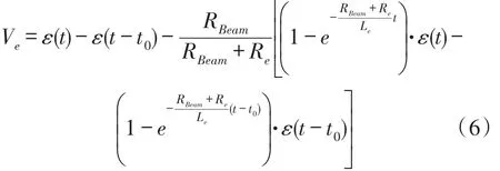
From the solution,we can find that when we give an ideal gate signal(impulse)to the system,the wave⁃form will suddenly rise and fall at rising and falling edg⁃es in a short time. Moreover,since the time constantis short because the plate capacitor is small as several pF,the waveform will show us a dis⁃tinct sharp peak at the rising and falling edges. On the contrary,we can deduce that the recovery time of the peak current will be longer when the plate capacitor is bigger,which have been proved in our experiments.
The simulation and experimental results can be maintained in Fig.4(a)and Fig.4(b).
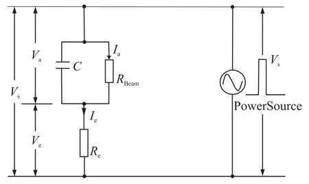
Fig.3 The ideal electronic-circuit to explain the capacitor effect

Fig.4 The influence of the plate capacitor(a)Simulation result(b)Experimental result
In the experiment,we substitute the field emis⁃sion tube with a capacitor matching the parameter of the tube,as show plate in Fig.3. Therefore,we can not only exclude the influence of the internal structure ofthe field emission tube,but make it available to change the capacitor to obtain the same experimental phenom⁃ena with the field emission tube.
2.2Measuring Resistance’s Parasitic Inductance To merely analyze the influence from the parasitic inductance,we idealize the circuit as Fig.5.

Fig.5 The ideal electronic-circuit analyzing the effect of parasitic inductance
In Fig.5,Leis the parasitic inductance of measur⁃ing resistance.
According to the electronic-circuit model,the fol⁃lowing equations can be obtained:

The solution to the equations is:
From the solution,we can figure out that the simi⁃lar situation will also appear if the time constant t=is short. Since Ris several MΩ and LBeameis very small and the recovery time will be pretty short,the oscilloscope will not be able to observe a distinct sharp peak,coinciding with the experimental results.
The simulation and experimental results can be maintained in Fig.6(a)and Fig.6(b).
Fig.6 The influence of the parasitic inductance(a)Simulation result(b)Experimental result
In the experiment,we directly link a big inductor after the measuring resistance without changing the cir⁃cuit structure in other aspects. In this case,if the sharp peak hikes dramatically after we connect the measur⁃ing resistance with a small inductor matching the para⁃sitic inductance of the resistance,we can conclude that the parasitic inductance also contributes to the peak.
However,the waveform remained unchanged when we added a small inductor to the measuring resis⁃tance while the distinguished sharp peaks emerged when adding a large one.
According to the theoretical calculation,we can convince our assumption that the oscilloscope cannot observe such distinct sharp peaks when the inductance is small while it can recognize with a larger enough in⁃ductance,because the time constant is shorter than the sampling rate of the oscilloscope.
In the simulation,we replace the field emission tube with a resistance to observe the results without any influence from the capacitor,as shown in Fig.5.
3 Results Analysis
According to the results,we can easily figure out that the plate capacitor make great contributions to the sharp peak. Meanwhile,the waveforms we get perfectly match the experiment phenomena of field emission tube,so that we can not only conclude the plate capaci⁃tor results in the sharp peak,but demonstrate the elec⁃tronic-circuit model of field emission tube rational.
On the other hand,when changing the source re⁃sistance and measuring one,we can easily observe a sharp peak at appropriate parameters,source and mea⁃suring resistance smaller than 100 Ω and the induc⁃tance larger than 1 mH .
Regardless of the frequency at the rising and fall⁃ing edges,only when the parasitic inductance of the measuring is larger than 100 H(resulting in the lon⁃ger enough time constant to observe the sharp peaks)can there form distinct sharp peaks at the rising and falling edges,which is unreasonable in our experimen⁃tal condition. Therefore,we can conclude that the main reason of sharp peaks is the plate capacitor of the field emission tube and the parasitic inductance almost doesn’t affect the waveform because the recovery time is too short to distinguish.
On the other hand,since we have proved that the inductor can produce sharp peaks,we can also utilize it to kill the sharp peaks.That is to say,the parasitic in⁃ductance will produce a sharp peak voltage in a pretty short period and we cannot observe them with the oscil⁃loscope. To effectively eliminate such sharp peaks,we have to connect a bigger inductor in the front circuit to draw all the voltage on it at the rising and falling edges.
4 Solution to Decrease of the Peak
4.1Adding a Choke at Load
As shown in Fig.7(a),by adding a choke(very high inductance to cut off the high frequency signal)at load,we can effectively reduce the peak current in the whole circuit,not by-pass the current of the measuring resistance. It is a very efficient way to protect the cir⁃ cuit as a whole because the global current will be limit⁃ed at rising and falling edges.
4.2Parallel Connecting a Capacitor
As shown in Fig.7(b),we can parallel connect a capacitor with the measuring resistance. The principle of this method has been introduced before,which is similar with the capacitor’s contribution to the sharp peak current. Since the capacitive reactance is small at the rising and falling edges,the measuring resistance can be regarded as short-circuited,capacitor by-pass⁃ing the high current,protecting the oscilloscope.
4.3Adding Low Pass Filter at Load
As shown in Fig.7(c),the load is a high-pass fil⁃ter. In order to kill the peaks,we can add a low-pass fil⁃ter at load to filter out the high frequency signal.
4.4Parallel Connecting a Diode
As shown in Fig.7(d),at the falling peaks,the di⁃ode will also short- circuit the measuring resistance,eliminating reverse sharp peak in the waveform.
The four solutions above have been experimented by our group respectively,and every one can contrib⁃ute to decreasing the sharp peaks to some extent. Then we experiment to combine these solutions,ob⁃taining comparative ideal waveform of circuit Ie,showing in Fig.7(b). From waveform in Fig.7(b),it can be seen that the sharp peaks on both rising and falling edges of pulse have been removed. The further investigation of impulse response of field-emission can be conducted.
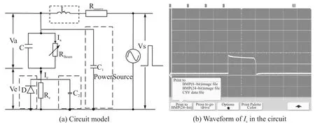
Fig.7 Electronics-circuit models of different solutions(a):(1)Add inductor at load;(2)Parallel capacitor;(3)Add a low-pass filter;(4)Parallel diode. (b)Waveform of circuit Ieafter using solutions in(a).
5 Conclusion
The causes of the sharp peaks are investigated by numerals simulations and experiments. By using a host of methods to demonstrate our assumptions,we have not only confirmed the influence of plate capacitor of the field emission tube to the sharp peak at the rising and falling peak,but excluded the effect of parasitic in⁃ductance when the source resistance and the measur⁃ing resistance are bigger than 10 kΩ,because the time constant of the sharp peak is too short to observe in such condition.
However,since the inductance has been proved to restrain the current value,we put forward the solution to series connect a choke on load to limit the instane⁃ous current change.
Moreover,by utilizing the bypassing characteris⁃tic of capacitor,we give the solution to parallel connect a capacitor on load or with the measuring resistance. Furthermore,we also replace the capacitor with a di⁃ode,attaining the similar consequence at the falling edge.
参考文献:
[1]Vink T J,Gillies M,Kriege J C. Enhanced Field Emission from Printed Carbon Nanotubes by Mechanical Surface Modification[J]Appl. Phys. Lett.,2003,83(17):3552-3554.
[2]Kim Y C,Sohn K H,Cho Y M,et al. Vertical Alignment of Print⁃ed Carbon Nanotubes by Multiple Field Emission Cycles[J]. Appl Phys Lett,2004,84(26):5350-5352.
[3]Kim J M,Choi W B,Lee N S. Field Emission from Carbon Nano⁃tubes for Displays[J]. Diamond Relat Mater,2000,9(3):1184-1189.
[4]Feng T,Zhang J,Li Q,et al. Effects of Plasma Treatment on Mi⁃crostructure and Electron Field Emission Properties of Screen-Printed Carbon Nanotube Films[J]. Phys E,2007,36(1):28-33.
[5]Kim J S,Ahn K S,Kim C O. Ultraviolet Laser Treatment of Multi⁃wall Carbon Nanotubes Grown at Low Temperature[J]. Appl Phys Lett,2003,82(10):1607-1609.
[6]Wang Z L,Gao R P,de Heer W A. In Situ Imaging of Field Emis⁃sion from Individual Carbon Nanotubes and Their Structural Dam⁃age[J]. Appl Phys Lett,2002,80(5):856-858.
[7]Lysenkov D,Müller G. Improved Current Densities of Carbon Nanotube Cathodes by Pulsed Operation[J]. Vac Sci Technol B,Microelectron Process Phenom,2006,24(2):1067-1071.
[8]Kim H J,Choi J J,Han J H. Design and Field Emission Test of Carbon Nanotube Pasted Cathodes for Traveling-Wave Tube Ap⁃plications[J]. IEEE Trans Electron Devices,2006,53(11):2674-2680.
[9]Spindt C A,Brodie I,Humphrey L,et al. Physical Properties of Thin- Film Field Emission with Molybdenum Cones[J]. Appl Phys,1976,47(12):5248-5263.
[10]Wang Q H,Corrigan T D,Dai J Y,et al. Field Emission from Nanotube Bundle Emitters at Low Fields[J]. Appl Phys Lett,1997,70(24):3308-3310.
刘春毅(1990-),男,汉族,江苏人,学东南大学电子科学与工程学院硕士,主要研究方向为基于碳纳米管场发射X射线系统,aystliu@163.com;

雷威(1967-),男,汉族,东南大学教授,主要研究方向为纳米材料、TFT、量子点技术,lw@seu.edu.cn。

Synthesis and Field Emission Properties of Diamond Microcrystalline*
GAO Jinhai1*,LI Zhen1,ZHANG Wuqin1,ZHANG Binlin2
(1.Department of Physics,Zhengzhou Normal University,Zhengzhou 450044,China;2.Physics Engineering College,Zhengzhou University,Zhengzhou 450052,China)
Abstract:The diamond microcrystalline films was fabricated by microwave plasma chemical vapor deposition(MP⁃CVD)method. The ceramic with a Ti mental layer was used as substrate. The fabricated diamond was evaluated by Raman scattering spectroscopy,X-ray diffraction spectrum(XRD),scanning electron microscopy(SEM). The field emission properties were tested by using a diode structure in a vacuum. A phosphor-coated indium tin oxide(ITO)anode was used for observing and characterizing the field emission. It was found that the diamond microcrystalline films exhibited good electron emission properties. The turn-on field was only 1.15 V/μm,and emission current den⁃sity as high as 0.81 mA/cm2was obtained under an applied field of 3.35 V/μm. The field emission properties of the diamond microcrystalline films are discussed relating to microstructure and electrical conductivity.
Key words:diamond microcrystalline films;field emission;emission site densities;chemical vapor deposition
doi:EEACC:0520;232010.3969/j.issn.1005-9490.2016.01.003
收稿日期:2015-02-05修改日期:2015-03-13
中图分类号:TN311
文献标识码:A
文章编号:1005-9490(2016)01-0006-06
猜你喜欢
学与玩(2022年8期)2022-10-31
河南科技(2022年8期)2022-05-31
化工管理(2021年7期)2021-05-13
铁道通信信号(2020年12期)2020-03-29
中国材料进展(2019年10期)2019-12-07
电子制作(2018年19期)2018-11-14
电子制作(2018年19期)2018-11-14
电子制作(2017年10期)2017-04-18
电子制作(2017年19期)2017-02-02
电子制作(2016年19期)2016-08-24