Design of an Operational Amplifier Using PSPICE
2016-10-18 00:27张海明
科技视界 2016年22期
张海明
【Abstract】This report demonstrates the experiment of operational amplifier design based on PSPICE software. The assignment contains three parts the first of which is to find transistor output characteristics,and the next is to set DC,transient and AC sweeps to find out the characteristics of the amplifier.The final part is to plot Bode plot to search the frequency response.The report will present the operation and results of each sections,and detailed analysis and discussion will also be provided.
1Introduction
1.1Objectives
The objective of this project is to design an operational amplifier and simulate it by PSPICE software.The amplifier has to satisfy the following requirements in design[1]:
a)The input impedance.
b)The output impedance.
c)The frequency response down to DC.
d)Output voltage to be approximately zero for zero input.
e)Total voltage consumption with voltage supply to be-9V to+9V.
1.2Theoretical Background
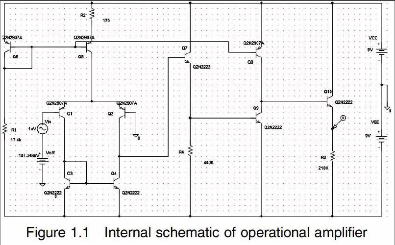
The operational amplifier is high-gain voltage amplification device and there are basically five parts included, the first of which is a differential amplifier with two differential inputs.The second part is the simple current mirror that sets the DC bias current.Whilst the next section is an emitter follower to reduce the load effect,which is followed by a common emitter that has a second amplification.The last part is another emitter follower to produce a low output impedance.The figure 1.1 below is the figure of the basic structure of an operational amplifier.
Figure 1.1Internal schematic of operational amplifier
2Methods
According to the circuit above,the process can be divided into several parts.The first I s to sketch the output characteristics via.Then find out the DC current gain and AC current gain respectively due to the characteristic of the sketch.
According to the design specifications to calculate the values of the resistors in the circuit.Then obtain the transfer characteristics by DC sweep to find out the DC working ranges and open loop gain,and voltage offset of the amplifier.Then operate the AC sweep to find out the input and output impedance.
3Results
3.1Transistor Output Characteristics
As explained in the Methods section that the target of this part is to estimate the DC current gain of NPN transistor.Firstly,the output characteristics of Q2N2222 NPN transistor can be found that the collectorcurrent varies due to the change of voltage and base current.Due to the set of from 0 to 40μA in steps of 4μA and the bottom is in=0 with top in=40μA.When current=2mA which is presented in the red line,it approximately matches the forth curve where=12μA so that the DC current gain at this point is
The AC current gain can be estimated by the deviation of divided by and the deviation of base current.Therefore,when holding the value of,the deviation of between two adjacent curves can be obtained.Therefore,the average value of AC current gain is
3.2Achieving Specification of Operational Amplifier
3.2.1Resistors Calculation
Table 3.1The value of Resistor from R1toR4.
3.2.2Open Loop Gain
According to the operational amplifier equation in the differential mode.
Where=0 is operated,so that the open loop gain is
Figure 3.1The output voltage VS input voltage
It can be seen that the slope of the curve is the open loop gain,so in the operating points A1 and A2,it has
3.2.3Transient Simulation
The transient simulation presents the output waveform varying via time.Therefore,the sine-wave voltage source is employed as the input the input frequency of which is set 1Hz. Form Figure 3.7 it can be found that the operating range of the input is about -6 to+6,so the amplitude of the input signal is set from -4 to+4 in steps of 1 to obtain a set of output waveforms.Figure 3.2 presents the waveform when then input amplitude is 1.
Figure 3.2Transient Output waveform
Therefore,the output amplitude is 1.3253V and the gain is about 1325300.Therefore,the average gain of the amplifier is
3.2.4Input and Output Resistance
The AC sweep presents the output varying via frequency.To find the input impedance,the VAC voltage source is employed with amplitude set from -4 to+4 in steps of 1 to obtain a set of impedances.At the same time,the trace is set as VAC/IAC to present input impedance.By calculation,the average input impedance is
This value is not same as what it is assumed as but close to that, which means that the values of resistors set are relatively correct.
To measure the output impedance,the input voltage source should be shorted and there should be an AC voltage source connected to the output terminal.The amplitude of this source is due to the input operation range and the open loop gain.Therefore,the amplitude is set from 1V to 5V in steps of 1V to obtain a set of output impedances.At the same time,the trace is set as VOUT/IOUT to present output impedance.By calculation, the average input impedance is
Similarly,this value differs from what it is set as.However,this value is close to the initial set which means that the resistors set and the offset voltage found are in the reasonable range.
3.3Frequency Response of the Operational Amplifier
The Bode plots contain the plot of both voltage gain and phase. Figure 3.3 presents the gain plot with respect to the frequency.
Figure 3.3Bode plot of the voltage gain
The function of this Bode plot of the voltage gain is
It can be seen from the figure that the AC voltage gain stabilizes in the low frequency region, and the value is about 122.517dB down to DC as the point A1 shows.
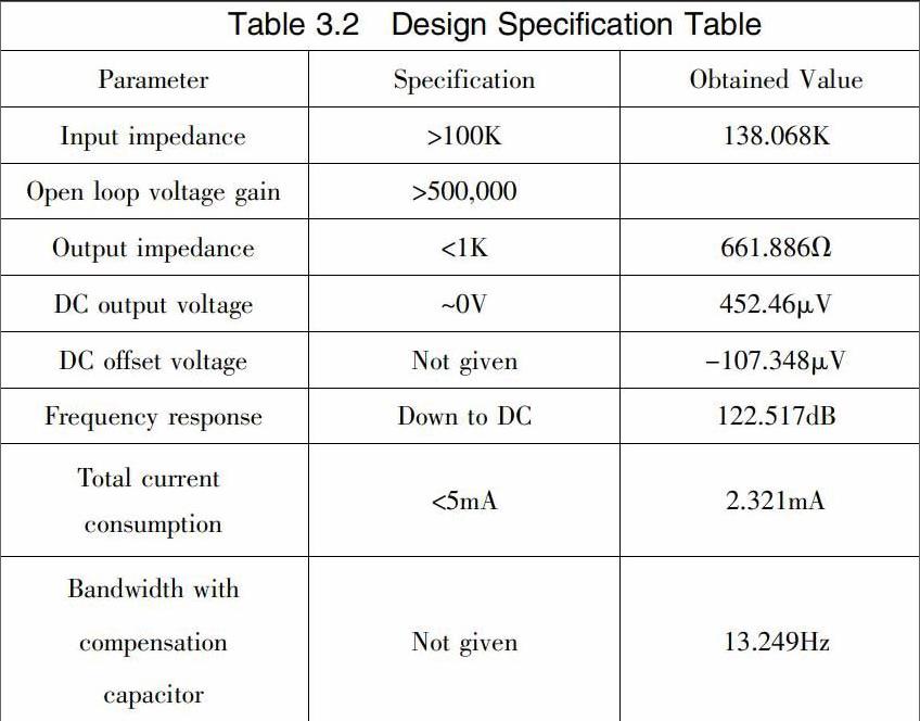
3.4Design Specifications Table
Table 3.2Design Specification Table
4Discussions
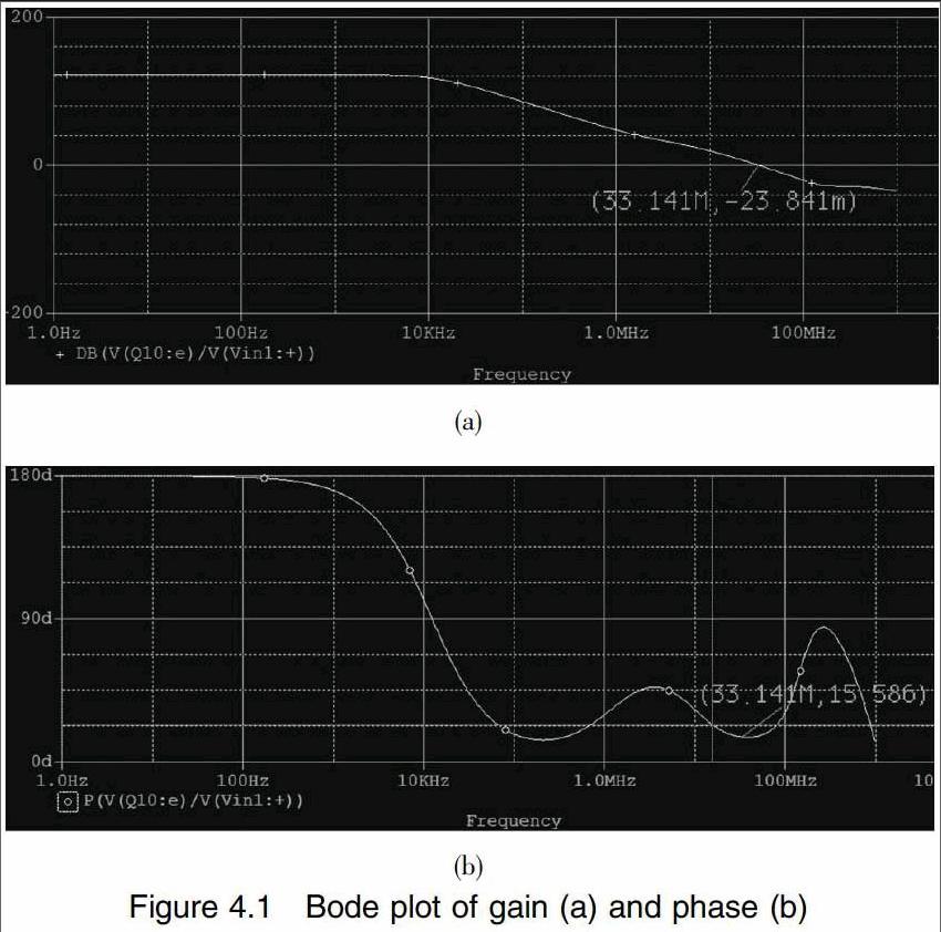
What can you deduce about the stability of your amplifier from the Bode plots in Part III?
The operational amplifier designed is an open loop system, the stability of which can be estimated by gain margin and phase margin from the Bode plot.Gain margin,a positive number,is the difference between 0dB and voltage gain where the frequency has a 180 degree phase difference.Phase margin is the difference between 180 degree and the phase shift where voltage gain crosses 0dB. Looking into Figure 3.3 that the phase difference cannot achieve 180 degree,so only phase margin is considered.Looking into Figure 4.1 for the phase margin.
(a)
(b)
Figure 4.1Bode plot of gain (a) and phase (b)
It can be seen that the gain crossover frequency is approximately 33.141 MHz in figure (a),so the corresponding phase in the figure(b)is about 15.586 degree and this is the phase margin as the phase plot starts at 180 degree.As the phase margin is 15.586 which is larger than zero so that this operational amplifier is stable.However,as the bigger the phase margin,the more stable of the amplifier,this amplifier is not much stable and the ideal range of phase margin is about 45 to 70 degree.
5Conclusions
In conclusion,the designed operational amplifier satisfy all the design requirement and is stable according to the phase margin and gain margin.At the same time,this operational amplifier has a high common mode rejection ratio(CMRR)in a millionaire level due to the small value of common mode gain.
Most importantly,this experiment is a practice of the analog circuits design with respect to the analog circuit design. The design process helps us have a deep understanding of the concepts we have learned and a better application.
【References】
[1]Ali.Al.Ataby,"Experiment 5 lab script,"[Online].Available: https://vital.liv.ac.uk/webapps/blackboard/content/listContent.jsp?course_id=_236259_1&content_id=_871458_1 [Accessed 27 4 2016].