
A 600W Broadband Doherty Power Amplifier with Improved Linearity for Wireless Communication System
2017-05-08 01:46JingLiWenhuaChenQianZhang
China Communications 2017年2期
Jing Li, Wenhua Chen, Qian Zhang
Department of Electronic Engineering, Tsinghua University, Beijing100084, China
* The corresponding author, email: chenwh@tsinghua.edu.cn
I. INTRODUCTION
With the evolution of communication standards, modern communication systems often require transmitters to work at multi-band or multi-standard operation efficiently. Besides,to reach higher data rate and spectral efficiency, complex modulation technique is employed, which results in high peak-to-average power ratio (PAPR). Power amplifier, which is used to amplify modulated signals, is a crucial part of the wireless transmitter and its performance affects the linearity and efficiency of the whole wireless communication systems.
Doherty power amplifier (DPA) is an attractive choice to amplify modulated signals due to its high average efficiency. A number of bandwidth extension techniques have been proposed in recent years due to the demand of communication systems for multi-band and multi-standard operation [1]- [11]. These modified DPAs achieved high back-off and peak efficiency as well as good linearity. However,the traditional Doherty architecture does not always work well for higher power application especially at frequencies around 2GHz which is the mainstream wireless communication bands. The optimal impedance of high power transistors is usually much lower than the characteristic impedance of the communication system which makes it difficult to design matching networks due to the large impedance transformation ratio. [12] presented a threestage high power DPA to extend the back-off range. And [13] presented a high efficiency 3W-DPA with Class-F topology. A 200W DPA is carefully designed considering both fundamental and the second harmonic optimal impedance in [14]. An asymmetric Doherty architecture easing the matching structures is presented in [15]. And authors in [16]- [19]designed several high power and high efficiency DPAs using semiconductor technology.However, most of these high power amplifiers worked at one single frequency and few literatures proposed wide-band high power ampli fiers using packaged transistors.
In general, there is a trade-off between efficiency and linearity especially for Doherty power amplifiers (DPAs). And DPAs with extended back-off range often have poor linearity which is difficult to be corrected even using digital pre-distortion algorithm. Therefore, it’s important to consider both high efficiency and good linearity for DPAs. Authors in [20] indicate that power amplifier devices contain more than one nonlinearity mechanism. Due to their interaction,the third order products IMD3 are affected not only by the fundamental component, but also the envelope and second harmonic frequenciesandIt means that the products at frequencyare added to the fundamental component atand contribute to the third order intermodulation products.
Usually, the bias network acts as an inductance at envelope frequency and parallel resonation occurs due to the parasitic capacitor of the packaged transistor. Generally, the parasitic capacitor varies with different devices and the equivalent inductance depends on the desired frequency. For mostly used Cree’s HEMT, the resonant frequency is at 100MHz level. And the mainstream communication bands are separated by 100MHz~700MHz. Once the resonant frequency is close to the differential frequency when the DPA is excited by two-tone signals and then the produced inter-modulated components leads to poor linearity.
The bandwidth from DC to this resonant frequency is defined as envelope bandwidth(EBW) by authors in this paper and in order to analyze its effect on linearity, the IMD2 and IMD3 is simulated and measured before and after extending EBW. And bandwidth, efficiency and linearity is discussed in detail on the basis of [21]. This paper is organized as follows: Section2.1 presents detailed analysis of the modified combining architecture and explain why this architecture has its advantage to design a wide-band and high efficiency power amplifier.Section2.2 defines the bandwidth from DC to the resonant frequency as envelope bandwidth(EBW) and the effect of EBW on concurrent multi-band performance of a broadband DPA is analyzed and Section2.3 provides several EBW extension techniques. Section3 presents the simulated and experimental results. Finally,conclusion is given in section4.
II. THEORETICAL ANALYSIS OF THE PROPOSED 3W-DPA
2.1 Analysis of the modified combining network
The proposed output combining network for high power 3W-DPA is shown in Fig.1.
According to the ABCD matrix of atransmission line, the drain voltage and current of carrier and peaking PA is written by

The fundamental component of the drain current and voltage of the carrier and peaking PAs versus the normalized input voltagepro-files are shown in Fig.2 whereis the maximum drain current and Vdc is the bias voltage.
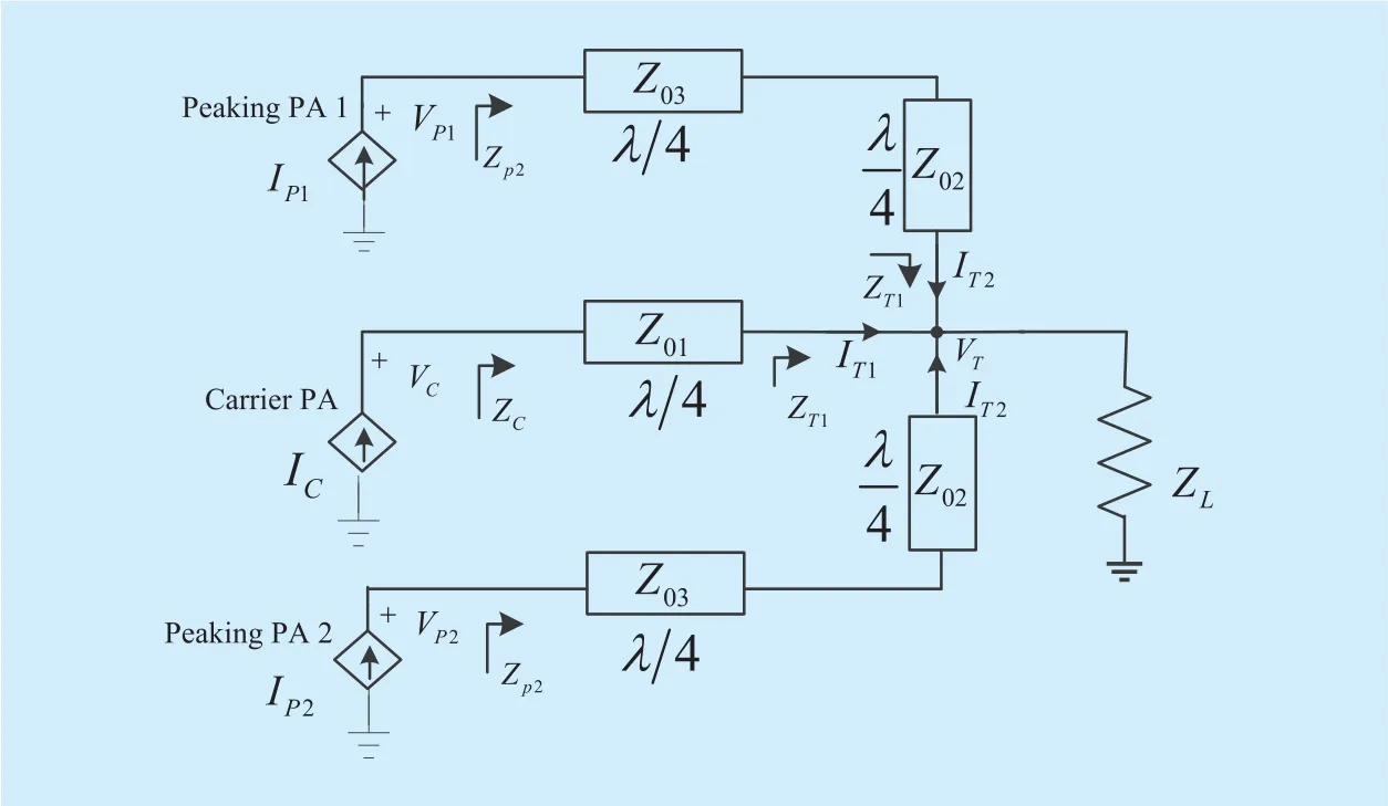
Fig.1 Modified combining network for high power 3W-DPA
As can be seen, the maximum magnitude of the output voltage equals the drain DC voltageand the maximum fundamental drain current is. Therefore, at the maximum output power level, equation (1) and (2) can be rewritten and simplified as

As the carrier and peaking PAs have the same optimal impedances, which arethenequalsat the saturation power level in Fig.1, and the impedancesandseen from the two peaking PAs at the combining node are three times of the load impedance.

The relation of the characteristic impedances of quarter-wave lines is derived from (3)and (4)

Therefore, the drain impedance of the carrier PA at the saturation output power level is

At low power region, the two peaking PAs is theoretically open at the combining node.The drain impedance of the carrier PA at the back-off output power level is


Fig.2 (a) Fundamental component of the drain current pro files versus normalized input voltage;(b) Fundamental component of the drain voltage profiles versus normalized input voltage
From (6) (7) and (8), there are four parameters,andtwo of which are free.Different load impedanceslead to different impedance bandwidth and letbe equal tothen there is

This proposed combining architecture provides a wide impedance bandwidth at back off output power level because the desired impedance of the transistor at 9.5dB back-off level is also equal toConsidering the bandwidth of the other two paths at high power level, we utilized two quarter-wave lines with different characteristic impedance and the values are set asBesides, post matching network is needed to match the load impedanceto the characteristic impedance of the RF transmitter.
2.2 Definition of envelope bandwidth for the broadband DPA
A simplified low frequency equivalent circuit of the bias network at the drain of the power amplifier is shown in Fig.3. Bias networks of power amplifiers often act as small inductances at envelope frequency and then form the parallel network together with the parasitic capacitor of the transistor. Bandwidth from DC to the resonant frequency is defined as envelope bandwidth (EBW).

Consider a broadband PA covering a frequency band fromtoas shown in Fig.4b. When this broadband PA is driven by two-tone Continuous Wave (CW) signals whose carrier frequencies areandthe
If the resonant frequency of the device is close to the differential frequency of two-tone concurrent input signals, and this parallel resonation produces a higher impedance seen from the ideal current source of the transistor which leads to concurrent performance degradation.
The contribution of products at envelope frequency to the total third order inter-modulation (IM3) can be seen from the composition of IM3 in Fig.4a.second order inter-modulation (IMD2) component falls into region I. Once the frequency differenceequals EBW, strong nonlinearity and reduced output power occurs.Therefore, EBW should be extended out of region I to guarantee a satisfying concurrent performance of the broadband PA.
2.3 EBW extension techniques
As multi-band concurrent performance of a broadband DPA deteriorates evidently due to the narrow EBW, measures must be taken in broadband DPA circuits to extend EBW.
The drain bias network is equivalent to an inductance at low frequency and forms parallel resonation together with the parasitic capacitor. From (10), although the parasitic capacitor cannot be changed, a conclusion still can be reached that a reduced equivalent inductance makes a higher resonant frequency which means a wider EBW. Then there are several practical tips to extend EBW of the broadband 3W-DPA based on above analysis.
2.3.1 Shorter micro-strip line of the bias network
Usually, the bias networks is amicro-strip line at RF frequency and its low frequency equivalent inductanceis proportional to its electrical length. Therefore, if the length of the micro-strip line is shorter than, the equivalent inductanceis also reduced. And then,the EBW of the proposed PA can be extended as expected.
2.3.2 Balanced DC supply network:
A balanced drain bias network provides two equivalent inductances in parallel, thus the effective inductance at the drain of transistor is also reduced. So the traditional single-stub micro-strip line can be replaced by balanced DC power supply network for wider EBW.

Fig.3 Simplified equivalent circuit of the bias network at the drain of the PA
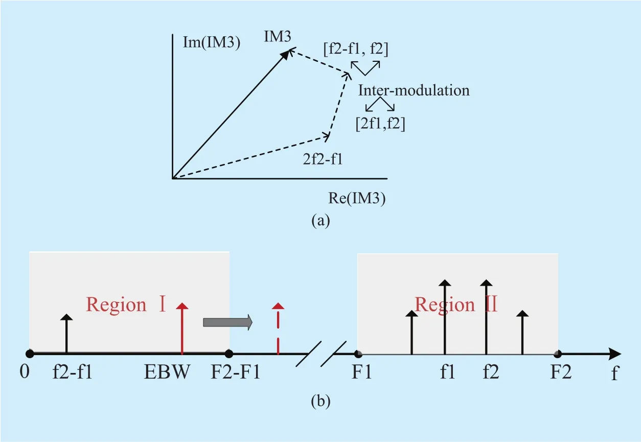
Fig.4 (a) Contribution of the second order inter-modulation to IM3; (b) Spectrum of broadband PA under two-tone excitation
As for the proposed broadband 3W-DPA,its schematic diagram is depicted in Fig.5a and the simplified diagram of the drain bias network is shown in Fig.5b. Three transistors in the circuit are powered by one voltage source placed at the end of the feeding line of thefirst peaking PA. Each section of transmission line in Fig.5b has the same length to simplify the analysis. LC equivalent networks at the drain of each transistor are also shown in Fig.5b.is an envelope decoupling capacitor. The feed line’s impedances at the drain of each transistor are expressed as follows.
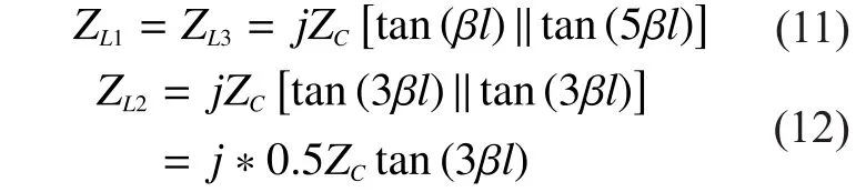

Fig.5 (a) Schematic diagram of the proposed 3W-DPA; (b) Simplified bias network of the proposed 3W-DPA; (c) Photograph of the proposed 3W-DPA

As can be seen, the LC networks resonate at a higher frequency and EBW of the threeway DPA is extended as well.
III. IMPLEMENTATION OF A BROADBAND 3W-DPA AND EXPERIMENTAL RESULTS
3.1 Design of the broadband 3W-DPA
Based on the theoretical analysis of the proposed three-way combining network for high power amplifiers, a broadband 3W-DPA using three CGHV22200 transistors is fabricated on a RF60 substrate as illustrated in Fig.5c. Its output matching network is modified slightly due to parasitic effects and the optimal impedance is decided by load-pull simulation. Besides, post matching network is used to match the load impedance to the system impedance.The bias network of the proposed 3W-DPA is marked with red line in Fig.5c. Large decoupling capacitors are added in the bias network to extend EBW. The gate of two peaking PAs is biased at -5.5V and the carrier PA is biased at -2.73V with 50V drain bias. The input power is divided equally by 3dB and 5dB hybrid couplers in cascade into the gate of these three transistors.
3.2 Simulated performance of the proposed 3W-DPA using continuous wave
The simulated result of the proposed 3W-DPA using continuous wave (CW) is shown in Fig.6a. As can be seen, its drain efficiency at back-off region is above 50% from 1.9 GHz to 2.2 GHz and the output power is about 600W with gains above 10dB. To verify the effect of EBW on the 3W-DPA’s two-tone concurrent performance, two-tone CW signal is used to excite this 3W-DPA. One frequencyisfixed,and the frequency intervalis swept from 40MHz to 180MHz. Simulated IMD2 and IMD3 versus frequency intervals are shown in Fig.7.
IMD2 and IMD3 varies with the frequency differenceand IMD3 atalmost gets close to the output power level at fundamental frequency which means strong nonlinearity and makes it hard to correct the nonlinearity of the DPA even with digital pre-distortion (DPD) algorithm. After employing EBW extension techniques mentioned above, Fig.7b shows that EBW is extended to 170MHz from 90 MHz and the worst IMD3 of 3W-DPA is also improved by about 9dB. Therefore, linearity of the broadband 3W-DPA is also improved.

Fig.6 (a) Simulated drain efficiency and power gain at different frequencies(b) Measured drain efficiency and power gain at different frequencies
3.3 Measured performance of the proposed 3W-DPA using continuous wave
Drain efficiency and power gain of this 3W-DPA is measured with a 10%-duty cycle pulse CW signal. As can be seen from Fig.7b,the designed 3W-DPA delivers 57.7dBm maximum output power. The back-off drain efficiency is above 45% from 2GHz to 2.2GHz while the efficiency decreases slightly to 35.5% at 1.9GHz and drain efficiency at saturation output power level is above 47.5%. In addition, the measured power gain is above 10dB across the whole band. The performance of this 3W-DPA is also compared with several high power amplifiers in table1.

Fig. 7(a) Simulated IMD2 before and after extending EBW versus frequency intervals; (b) Simulated IMD3 before and after extending EBW versus frequency intervals

Table I Comparison with three-way high power Doherty PA
To measure the concurrent performance of the designed broadband DPA, two-tone CW signals with the same input power are used to feed into the input port of this 3W-DPA. Thefirst frequencyisfixed on 1.92GHz and the second frequencychanges from 1.96GHz to 2.1GHz. Measured IMD2 and IMD3 are shown in Fig.8, which indicates the measured EBW is extended to 120 MHz from 70MHz and the worst IMD3 of proposed 3W-DPA is improved by about 5dB.
3.4 Measured results using twotone modulated signals
Then the 3W-DPA is also excited by two-tone modulation signals and the measured adjacent channel power ratio (ACPR) versus carrier frequency intervalsshown in Fig.9a suggests that linearity of this high power amplifier is improved by 5dB.
Finally, the concurrent power spectrum density (PSD) of this 3W-DPA measured with two-tone LTE signals at frequency 1.92 GHz and 2.01 GHz is shown in Fig.9b. EBW extension techniques are employed in this circuit to improve linearity, so ACPR is easily decreased under -45dBc at these two frequencies after applying digital pre-distortion (DPD).
IV. CONCLUSION
It is a great challenge to synthesize a broadband network for high power DPA as the optimal impedance of a high power transistor is much lower. Hence, modified combing network suitable to high power Doherty power amplifier is proposed and analyzed in this paper. Impedance bandwidth of this combining network varies with different load impedances.The proposed high power 3W-DPA is carefully designed considering both bandwidth and design complexity.
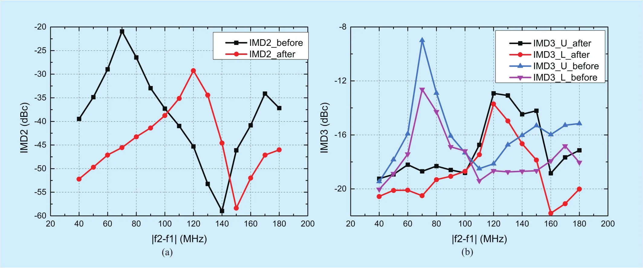
Fig.8 (a) Measured IMD2 before and after extending EBW versus frequency intervals; (b) Measured IMD3 before and after extending EBW versus frequency intervals

Fig.9 (a) Measured ACPR before and after extending EBW versus frequency intervals; (b) Measured concurrent spectrum at 1.92GHz and 2.01GHz with and without 2D-DPD after extending EBW
In addition, EBW is defined as the resonant frequency in this paper. When a broadband DPA is used to amplify two-tone modulated signals, narrow EBW results in strong nonlinearity especially under condition that carrier frequency interval equals EBW. Several EBW extension techniques are provided to improve the concurrent performance such as employing shorter micro-strip lines and balanced supply bias networks. Finally, EBW of this broadband 3W-DPA is extended to 120MHz from 70MHz and its linearity is also improved by about 5dB.
This work was supported in part by the National Basic Research Program of China(Grant No. 2014CB339900), the National Science and Technology Major Project of the Ministry of Science and Technology of China (Grant No. Grant 2015ZX03002002 and Grant 2016ZX03002009, and Grant 2016ZX03001005), the 863 program (Grant No. 2015AA010802), the National Natural Science Foundation of China (Grant No.61522112, 61331003), and the New Century Excellent Talents in University (NCET).
[1] D. Y. T. Wu and S. Boumaiza, “A Modified Doherty Con figuration for Broadband Ampli fication Using Symmetrical Devices,”IEEE Trans.Microw. Theory Tech., vol. 60, no. 10, pp. 3201-3213, Oct. 2012.
[2] R. Giofré, L. Piazzon, P. Colantonio and F. Giannini, “A Doherty Architecture with High Feasibility and Defined Bandwidth Behavior,”IEEE Trans.Microw. Theory Tech., vol. 61, no. 9, pp. 3308-3317, Sept. 2013.
[3] G. Sun and R. H. Jansen, “Broadband Doherty Power Amplifier via Real Frequency Technique,”IEEE Trans. Microw. Theory Tech., vol. 60, no. 1,pp. 99-111, Jan. 2012
[4] J. M. Rubio, J. Fang, V. Camarchia, et al, “3–3.6-GHz Wideband GaN Doherty Power Amplifier Exploiting Output Compensation Stages,”IEEE Trans. Microw. Theory Tech., vol. 60, no. 8, pp.2543-2548, Aug. 2012
[5] H. Golestaneh, F. A. Malekzadeh and S. Boumaiza, “An Extended-Bandwidth Three-Way Doherty Power Amplifier,”IEEE Trans. Microw. Theory Tech., vol. 61, no. 9, pp. 3318-3328, Sept. 2013
[6] C. M. Andersson, D. Gustafsson, J. Chani Cahuana, et al, “A 1–3-GHz Digitally Controlled Dual-RF Input Power-Amplifier Design Based on a Doherty-Outphasing Continuum Analysis,”IEEE Trans. Microw. Theory Tech., vol. 61, no. 10, pp.3743-3752, Oct. 2013
[7] M. N. A. Abadi, H. Golestaneh, H. Sarbishaei and S. Boumaiza, “An extended bandwidth Doherty power amplifier using a novel output combiner,”2014 IEEE MTT-S International Microwave Symposium (IMS2014), Tampa, FL, 2014, pp. 1-4.
[8] R. Giofrè, L. Piazzon, P. Colantonio,et al, “A Closed-Form Design Technique for Ultra-Wideband Doherty Power Amplifiers,”IEEE Trans.Microw. Theory Tech., vol. 62, no. 12, pp. 3414-3424, Dec. 2014.
[9] X. H. Fang and K. K. M. Cheng, “Improving Power Utilization Factor of Broadband Doherty Amplifier by Using Bandpass Auxiliary Transformer,”IEEE Trans. Microw. Theory Tech., vol. 63, no. 9,pp. 2811-2820, Sept. 2015.
[10] R. Kalyan, K. Rawat and S. K. Koul, “Design strategy of concurrent multi-band Doherty power amplifier,”IET Microwaves, Antennas & Propagation, vol. 9, no. 12, pp. 1313-1322, 9 17 2015
[11] J. Pang, S. He, C. Huang, et al, “A Post-Matching Doherty Power Amplifier Employing Low-Order Impedance Inverters for Broadband Applications,”IEEE Trans. Microw. Theory Tech., vol. 63,no. 12, pp. 4061-4071, Dec. 2015.
[12] M. J. Pelk, W. C. E. Neo, J. R. Gajadharsing,et al, “A High-Efficiency 100-W GaN Three-Way Doherty Amplifier for Base-Station Applications,”IEEE Trans. Microw. Theory Tech., vol. 56, no. 7, pp.1582-1591, July 2008
[13] J. Moon, J. Kim, I. Kim, et al, “Highly Efficient Three-Way Saturated Doherty Amplifier with-Digital Feedback Predistortion,”IEEE Trans.Microw. Theory Tech., vol. 18, no. 8, pp. 539-541,Aug. 2008.
[14] K. Bathich, M. T. Arnous and G. Boeck, “Design of 200 W wideband Doherty amplifier with 34% bandwidth,”2013 European Microwave Conference, Nuremberg, 2013, pp. 279-282.
[15] J. Staudinger, G. Bouisse and J. Kinney, “High efficiency 450W asymmetric three-device Doherty amplifier with digital feedback predistortion,”2010 IEEE Radio and Wireless Symposium (RWS),New Orleans, LA, 2010, pp. 116-119.
[16] S. Embar R., L. Wang, J. Kim, et al, “A 400 W 2-way asymmetrical doherty PA with 50% efficiency based on second-generation airfastTMLDMOS technology,”2015 IEEE Topical Conference on Power Amplifiers for Wireless and Radio Applications (PAWR), San Diego, CA, 2015, pp. 1-3.
[17] J. Kim, B. Fehri, S. Boumaiza and J. Wood, “Power Efficiency and Linearity Enhancement Using Optimized Asymmetrical Doherty Power Amplifiers,”IEEE Trans. Microw. Theory Tech., vol. 59,no. 2, pp. 425-434, Feb. 2011.
[18] H. Deguchi, N. Watanabe, A. Kawano, et al, “A 2.6GHz band 537W peak power GaN HEMT asymmetric Doherty amplifier with 48% drain efficiency at 7dB,”2012 IEEE/MTT-S International Microwave Symposium Digest, Montreal, QC,Canada, 2012, pp. 1-3.
[19] T. Landonet al., “Design of a 600W Doherty using generation 2 HVHBT with 55% WCDMA efficiency linearized to −55dBc for 2c11 6.5dB PAR,”2012 IEEE Topical Conference on Power Amplifiers for Wireless and Radio Applications,Santa Clara, CA, 2012, pp. 73-76.
[20] Vuolevi J, Rahkonen T. Distortion in RF power amplifiers[M]. Artech house, 2003.
[21] Jing Li, Jianli Liu, Wenhua Chen, Gongzhe Su and Zonghao Wang, “A 600W broadband threeway Doherty power amplifier for multi-standard wireless communications,” 2015 IEEE MTT-S International Microwave Symposium, Phoenix,AZ, 2015, pp. 1-3.
[22] H. Kang; H. Lee; H. Oh; W. Lee; C. s. Park; K. C.Hwang; K. Y. Lee; Y. Yang, “Symmetric Three-Way Doherty Power Amplifier for High Efficiency and Linearity,”IEEE Transactions on Circuits and Systems II: Express Briefs, vol.PP, no.99,pp.1-1

- China Communications的其它文章
- Open Access Strategy in Cloud Computing-Based Heterogenous Networks Constrained by Wireless Fronthaul
- Orchestrating Network Functions in Software-Defined Networks
- RGB Based Multiple Share Creation in Visual Cryptography with Aid of Elliptic Curve Cryptography
- Distributed Document Clustering Analysis Based on a Hybrid Method
- Action Recognition with Temporal Scale-Invariant Deep Learning Framework
- High-Performance Beamformer and Low-Complexity Detector for DF-Based Full-Duplex MIMO Relaying Networks