
Ultrafast interlayer photocarrier transfer in graphene–MoSe2 van der Waals heterostructure∗
2017-08-30 08:26XinWuZhang张心悟DaWeiHe何大伟JiaQiHe何佳琪SiQiZhao赵思淇ShengCaiHao郝生财YongShengWang王永生andLiXinYi衣立新
Chinese Physics B 2017年9期
关键词:大伟
Xin-Wu Zhang(张心悟),Da-Wei He(何大伟),Jia-Qi He(何佳琪),Si-Qi Zhao(赵思淇),Sheng-Cai Hao(郝生财), Yong-Sheng Wang(王永生),and Li-Xin Yi(衣立新)
Key Laboratory of Luminescence and Optical Information,Ministry of Education,Institute of Optoelectronic Technology,
Beijing Jiaotong University,Beijing 100044,China
Ultrafast interlayer photocarrier transfer in graphene–MoSe2van der Waals heterostructure∗
Xin-Wu Zhang(张心悟),Da-Wei He(何大伟),Jia-Qi He(何佳琪),Si-Qi Zhao(赵思淇),Sheng-Cai Hao(郝生财), Yong-Sheng Wang(王永生),and Li-Xin Yi(衣立新)†
Key Laboratory of Luminescence and Optical Information,Ministry of Education,Institute of Optoelectronic Technology,
Beijing Jiaotong University,Beijing 100044,China
We report the fabrication and photocarrier dynamics in graphene–MoSe2heterostructures.The samples were fabricated by mechanical exfoliation and manual stacking techniques.Ultrafast laser measurements were performed on the heterostructure and MoSe2monolayer samples.By comparing the results,we conclude that photocarriers injected in MoSe2of the heterostructure transfer to graphene on an ultrafast time scale.The carriers in graphene alter the optical absorption coefficient of MoSe2.These results illustrate the potential applications of this material in optoelectronic devices.
van der Waals heterostructure,transition metal dichalcogenides,molybdenum diselenide,transient absorption
1.Introduction
The discovery of graphene in 2004[1,2]has stimulated extensive studies on its novel property and potential applications. Graphene is formed by a single layer of carbon atoms bound together in a hexagonal lattice.Due to its unique structure, graphene has many superior properties,such as high Young’s modulus and fracture strength,[3]high thermal conductivity,[4]ultrafast dynamic optical properties,[5]and high charge carrier mobility.[1]These properties make graphene an attractive candidate for various applications,such as ultracapacitors,[6,7]solar cells,[8–11]photodetector,[12]and low-power-consumption electronics.[13,14]However,the lack of a bandgap limited its application in logic electronic devices.Furthermore,its relatively small optical absorbance is also a drawback for optoelectronic applications.Monolayer transition metal dichalcogenides(TMDs),on the other hand,have remarkably high absorbance in the visible range[15]and a sizable bandgap.[16,17]However,their charge carrier mobilities are relatively low. Hence,combining graphene and TMD can potentially produce bi-layer materials that can effectively absorb light and transfer charge carriers,which are two key elements for most optoelectronic applications.
Indeed,very recently,significant progress has been made in studies of graphene–TMD heterostructures.So far,most studies have focused on combining graphene with MoS2. Initially,such heterostructures were fabricated by manually stacking graphene and MoS2monolayers together.[18]Mechanical properties of graphene–MoS2were studied both theoretically and experimentally.[19,20]The electronic structure of the formed heterostructure was calculated,measured,and controlled.[21–26]For electronic applications,tunneling transistors have been demonstrated with MoS2serving as the tunneling barrier.[18,27–33]
Besides these investigations on graphene–MoS2,heterostructure formed by graphene and tungsten based TMD monolayers has also been studied.For graphene–WS2,spin–orbit interaction[34]and various applications have been attempted,such as tunneling transistors,[29,35]photovoltaics,[36]light-emitting diodes,[37]and photodetection.[38]Measurements of its band alignment,[39]photoluminescence properties,[40]and light-emitting devices[37]have been reported.
In contrast to these extensive efforts on developing heterostructures formed by graphene and MoS2and WS2,MoSe2has been seldom used to form heterostructures with graphene. The only reports on graphene–MoSe2heterostructures are their molecular beam expitaxy[41]and observation of photoluminescence quenching.[42]MoSe2possesses several properties that make it an attractive member of TMDs.It has a direct optical bandgap of 1.55 eV,[43]which is near the optimal bandgap of single-junction photovoltaic devices and photocatalysis.[44–46]
Here we report fabrication of graphene–MoSe2heterostructures and ultrafast laser measurements on photocarrier dynamics.We observed efficient carrier transfer from MoSe2to graphene,and strong effect of carriers in graphene on optical properties of MoSe2.These results indicate that graphene–MoSe2heterostructures are promising materials for optoelectronic applications.
2.Experiment
Graphene and MoSe2flakes were fabricated by mechanical exfoliation.Adhesive tapes were used to mechanically exfoliate flakes from bulk crystals onto polydimethylsiloxane (PDMS)substrates.The monolayers were identified by optical contrasts with an optical microscope.Then a MoSe2monolayer flake was transferred to a Si substrate with a 90 nm SiO2layer and annealed for 2 h at 200°C in an Ar(60 sccm) environment with a pressure of 3 Torr.Next,a graphene flake was transferred onto the MoSe2flake,followed by the same annealing procedure.The final optical microscope image of the sample is shown in Fig.1(a),where the graphene–MoSe2heterostructure is in the triangle yellow area.Figure 1(b)illustrates the predicted band alignment[47,48]of the heterostructure.We note that the band gap of MoSe2presented in Fig.1(b)is a theoretical value,which is different from that of the experiment and has no influence on the measurement.
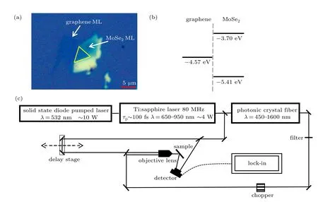
Fig.1.(color online)(a)Microscope images of the samples studied.(b)Band alignment of graphene and MoSe2 monolayers.(c)Experimental setup to measure differential reflectivity.
In the transient absorption microscopy setup shown as Fig.1(c),a passively mode-locked Ti:sapphire oscillator was used to generate a 100 fs pulse with a central wavelength of 790 nm at 80 MHz.We used a beamsplitter to separate the pulse into two beams.One of the beams was coupled to a photonic crystal fiber to generate supercontinuum.A bandpassfilter with a passing wavelength of 620 nm and a bandwidth of 10 nm was employed to select a 620 nm pulse from the super continuum,which served as the pump.Combined with the other beam probe which was outputted directly from the oscillator,the two beams were finally focused onto the sample by a microscope objective lens.The reflected probe was collimated by the objective lens and measured by one detector of a balanced detector.A portion of the probe beam was taken as a reference beam,which is sent to the other detector of the balanced detector.A lock-in amplifier was used to measure the voltage output of the detector.A mechanical chopper was placed in the pump arm to modulate the intensity of the pump beam at about 2 kHz.Hence,the balanced detector now outputs a voltage that is proportional to a differential reflectivity of the probe,R/R0.It is defined as the relative change of the probe reflectivity caused by the pump,(R-R0)/R0,where R and R0are the reflectivity of the probe with the pump presence and without it,respectively.All the measurements were performed at room temperature with the sample exposed in air.
3.Results and discussion
We first studied a MoSe2monolayer sample.A pump pulse of 2.00 eV was used to inject photocarriers.A probe pulse of 1.57 eV,which is tuned near to the exciton resonance of MoSe2,was used to monitor these photocarriers.The top panel of Fig.2(a)shows the differential reflectivity signal as a function of the probe delay.In this measurement,the pump fluence is 4.9µJ/cm2.By using an absorption coeffi-cient of 2×105cm−1for MoSe2monolayer at the probe photon energy,[49]an injected carrier density of 2.1×1010cm−2was established.A peak differential reflectivity signal of 1.14×10⁻⁴was observed.Furthermore,the decay of the signal can be fitted by a bi-exponential function,with two time constants of 22 and 125 ps,respectively.The rest of Fig.2(a) shows the measured signal at different pump fluences.By fitting these data,we found that as the pump fluence decreased, the fast decay component characterized by 22 ps becomes less pronounced.Based on this feature,we can attribute the long time constant of 125 ps to the photocarrier lifetime in MoSe2. The fast decay channel at higher fluence can be attributed to the contribution of exciton–exciton annihilation.[50]
Figure 2(b)summarizes the peak differential reflectivity signal as a function of the pump fluence.A linear relation is clearly observed,as confirmed by the linear fit(red line). Finally,with a fixed pump fluence of 1.23µJ/cm2,we repeated the measurement with different probe photon energies. Figure 2(c)shows the peak differential reflectivity signal as a function of the probe photon energy.The peak signal was observed at a probe photon energy of 1.57 eV,which is well consistent with the previously determined optical bandgap of MoSe2monolayers.This observation shows that the probe pulse senses the photocarriers via the change of the excitonic absorption peak induced by these carriers.
Figure 3 shows the results of the same measurement performed with the graphene–MoSe2heterostructure.If there was no interlayer photocarrier transfer or no interlayer coupling, the results should have been similar to those shown in Fig.2. Due to the smaller absorption coefficient of graphene compared to MoSe2,the carriers injected in graphene can be neglected for simplicity,and the pump pulse can be assumed to inject the same carrier density in the MoSe2of the heterostructure as the MoSe2monolayer.However,we observed two dramatic differences between the two measurements.First, the signal magnitude is about a factor of 10 larger in the heterostructure sample under the same conditions.Second,the signal decays rapidly compared to the MoSe2monolayer.Exponential fits(blue curves)produced a decay time constant of 8.5 ps.Meanwhile,similar dependences on the pump fluence and probe photon energy are observed.
We attribute these observed features to two physical mechanisms.First,the photocarriers excited in MoSe2rapidly transfer to graphene.Second,the carriers in graphene can induce a differential reflectivity signal of the probe tuned to the MoSe2resonance.
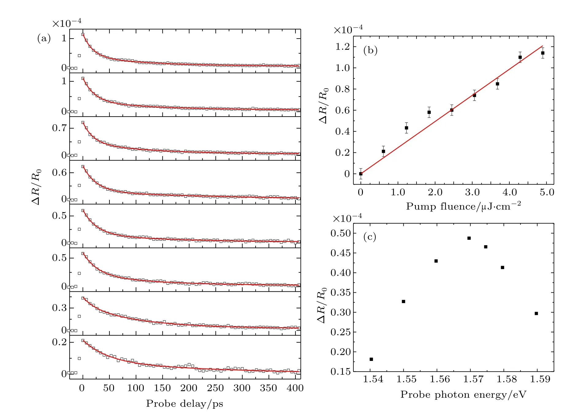
Fig.2.(color online)Differential reflectivity measurement of monolayer MoSe2.(a)Differential reflectivity signal as a function of probe delay with pump fluences of(from top to bottom)4.9,4.29,3.06,2.45,1.84,1.23 and 0.61µJ/cm2,respectively.The red curves are exponential fits.(b)Peak differential reflectivity signal as a function of pump fluence.(c)Peak differential reflectivity signal as a function of the probe photon energy.

Fig.3.(color online)Differential reflectivity measurement of graphene–MoSe2 heterostructure.(a)Differential reflectivity signal as a function of probe delay with pump fluences of(from top to bottom)4.9,4.29,3.06,2.45,1.84 and 1.23µJ/cm2,respectively.The blue curves are exponential fits.(b)Peak differential reflectivity signal as a function of pump fluence.(c)Peak differential reflectivity signal as a function of the probe photon energy.

Fig.4.The electric field of the excitons in MoSe2 before and after forming the heterostruture.
The strong dependence of the peak signal on probe photon energy indicates that the signal originates from a change of the absorption coefficient of MoSe2.However,this change cannot be induced by the photocarriers in MoSe2,since in the measurements on MoSe2monolayer(Fig.2),we have established the magnitude of the signal for such photocarrier densities used in the measurements.The signal is too large to be attributed to photocarriers in MoSe2.Furthermore,the decay of the signal is very fast.Since the lifetime of photocarriers in graphene was known to be on the same time scale,this further indicates that the signal monitors the carriers in graphene, instead of MoSe2.
We assume that the mechanism for change of the absorption coefficient of MoSe2by carriers in graphene is via a screening effect of these carriers on the electric field of the excitons.It has been well established that the Coulomb interaction between electrons and holes in monolayer TMDs is significantly enhanced by the reduced dielectric screening. As shown in Fig.4,the majority of the field lines are in the vacuum surrounding the monolayer.This effect has resulted in extremely large exciton binding energies in these materials.When combined with a graphene layer,the carriers in graphene can screen the fields in that layer,and hence change the interaction between the electrons and holes in excitons.
Therefore,our results provide quantitative information on the physics mechanism of screening of graphene on manybody interactions in MoSe2monolayers.In particular,it is possible to control the electron–hole interaction in MoSe2,as well as other 2D materials,by interfacing with graphene with a certain thickness.This opens up the opportunities of controlling electron–hole interactions in van der Waals materials.
Based on this mechanism and the fast decay of the signal observed in Fig.3,as well as the lack of a long-lived signal,we conclude that photocarriers excited in MoSe2rapidly transfer to graphene.These carriers in graphene can alter the absorption of MoSe2.
The observed effects have important implications on using these materials in optoelectronic devices.For example, the efficient transfer of photocarriers from MoSe2to graphene suggests that such bilayers can be used in photodetectors and solar cells.MoSe2has a large absorption coefficient at optimal wavelength for solar cells,while graphene possesses superior charge transport performance.The bilayer structure effectively combines these advantages.The demonstrated control of MoSe2absorption by carriers in graphene can be utilized in light modulation applications where gate controlled carriers in graphene can be used to modulate absorption of light by MoSe2.
4.Conclusion
We have fabricated a less investigated graphene–MoSe2heterostructure,and studied its photocarrier dynamics.We found that photocarriers injected in MoSe2transfer to graphene on an ultrafast time scale.We also found that a carrierin graphene can change the excitonic absorption ofMoSe2, which can be potentially used for electric control of optical absorption of MoSe2.Ourresults illustrate thatgraphene–MoSe2heterostructures can effectively combine the novel optical absorption property of MoSe2and charge the transport property of graphene,for potential applications in optoelectronic devices.
[1]Novoselov K S,Geim A K,Morozov S V,Jiang D,Zhang Y,Dubonos S V,Grigorieva I V and Firsov A A 2004 Science 306 666
[2]Novoselov K S,Geim A K,Morozov S V,Jiang D,Katsnelson M I, Grigorieva I V,Dubonos S V and Firsov A A 2005 Nature 438 197
[3]Lee C,Wei X,Kysar J W and Hone J 2008 Science 321 385
[4]Balandin A A,Ghosh S,Bao W,Calizo I,Teweldebrhan D,Miao F and Lau C N 2008 Nano Lett.8 902
[5]Jin Q,Dong HM,Han Kand Wang XF 2015 Acta Phys.Sin.64 237801 (in Chinese)
[6]Stoller M D,Park S,Zhu Y,An J and Ruoff R S 2008 Nano Lett.8 3498
[7]Pan D,Wang S,Zhao B,Wu M,Zhang H,Wang Y and Jiao Z 2009 Chem.Mater.21 3136
[8]Becerril H A,Mao J,Liu Z,Stoltenberg R M,Bao Z and Chen Y 2008 ACS Nano 2 463
[9]Chen H,Müller M B,Gilmore K J,Wallace G G and Li D 2008 Adv. Mater.20 3557
[10]Wang X,Zhi L and Müllen K 2008 Nano Lett.8 323
[11]Liu Z,Liu Q,Huang Y,Ma Y,Yin S,Zhang X,Sun W and Chen Y 2008 Adv.Mater.20 3924
[12]Liang Z J,Liu H X,Niu Y X and Yin Y H 2016 Acta Phys.Sin.65 138501(in Chinese)
[13]Geim A K and Novoselov K S 2007 Nat.Mater.6 183
[14]Geim A K 2009 Science 324 1530
[15]Liu H L,Shen C C,Su S H,Hsu C L,Li M Y and Li L J 2014 Appl. Phys.Lett.105 201905
[16]He K,Kumar N,Zhao L,Wang Z,Mak K F,Zhao H and Shan J 2014 Phys.Rev.Lett.113 026803
[17]Zeng F,Zhang W B and Tang B Y 2015 Chin.Phys.B 24 097103
[18]Britnell L,Gorbachev R,Jalil R,Belle B,Schedin F,Mishchenko A, Georgiou T,Katsnelson M,Eaves L and Morozov S 2012 Science 335 947
[19]Jiang J W and Park H S 2014 Appl.Phys.Lett.105 033108
[20]Elder R M,Neupane M R and Chantawansri T L 2015 Appl.Phys.Lett. 107 073101
[21]Ebnonnasir A,Narayanan B,Kodambaka S and Ciobanu C V 2014 Appl.Phys.Lett.105 031603
[22]Coy Diaz H,Avila J,Chen C,Addou R,Asensio M C and Batzill M 2015 Nano Lett.15 1135
[23]Jin W,Yeh P C,Zaki N,Chenet D,Arefe G,Hao Y,Sala A,Mentes T O,Dadap J I and Locatelli A 2015 Phys.Rev.B 92 201409
[24]Pierucci D,Henck H,Avila J,Balan A,Naylor C H,Patriarche G, Dappe Y J,Silly M G,Sirotti F and Johnson A C 2016 Nano Lett. 16 4054
[25]Ulstrup S,Čabo A G,Miwa J A,Riley J M,Grønborg S S,Johannsen J C,Cacho C,Alexander O,Chapman R T and Springate E 2016 ACS Nano 10 6315
[26]Wei Y,Ma XG,Zhu L,He H and Huang CY 2017 Acta Phys.Sin.66 087101(in Chinese)
[27]Yu W J,Li Z,Zhou H,Chen Y,Wang Y,Huang Y and Duan X 2013 Nat.Mater.12 246
[28]Moriya R,Yamaguchi T,Inoue Y,Morikawa S,Sata Y,Masubuchi S and Machida T 2014 Appl.Phys.Lett.105 083119
[29]Yamaguchi T,Moriya R,Inoue Y,Morikawa S,Masubuchi S,Watanabe K,Taniguchi T and Machida T 2014 Appl.Phys.Lett.105 223109
[30]Zhang W,Chuu C P,Huang J K,Chen C H,Tsai M L,Chang Y H, Liang C T,Chen Y Z,Chueh Y L and He J H 2014 Sci.Rep.4 3826
[31]Moriya R,Yamaguchi T,Inoue Y,Sata Y,Morikawa S,Masubuchi S and Machida T 2015 Appl.Phys.Lett.106 223103
[32]Sata Y,Moriya R,Morikawa S,Yabuki N,Masubuchi S and Machida T 2015 Appl.Phys.Lett.107 023109
[33]Joiner C A,Campbell P M,Tarasov A A,Beatty B R,Perini C J,Tsai M Y,Ready W J and Vogel E M 2016 ACS Appl.Mater.Inter.8 8702
[34]Wang Z,Ki D K,Chen H,Berger H,MacDonald A H and Morpurgo A F 2015 Nat.Commun.6 9339
[35]Georgiou T,Jalil R,Belle B D,Britnell L,Gorbachev R V,Morozov S V,Kim YJ,Gholinia A,Haigh S J and Makarovsky O 2013 Nat. Nanotechnol.8 100
[36]Shanmugam M,Jacobs-Gedrim R,Song E S and Yu B 2014 Nanoscale 6 12682
[37]Withers F,Del Pozo-Zamudio O,Mishchenko A,Rooney A,Gholinia A,Watanabe K,Taniguchi T,Haigh S,Geim A and Tartakovskii A 2015 Nat.Mater.14 301
[38]Tan H,Fan Y,Zhou Y,Chen Q,Xu W and Warner J H 2016 ACS Nano 10 7866
[39]Kim K,Larentis S,Fallahazad B,Lee K,Xue J,Dillen D C,Corbet C M and Tutuc E 2015 ACS Nano 9 4527
[40]Li Y,Qin J K,Xu C Y,Cao J,Sun Z Y,Ma L P,Hu PA,Ren W C and Zhen L 2016 Adv.Funct.Mater.26 4319
[41]Vishwanath S,Liu X,Rouvimov S,Mende P C,Azcatl A,McDonnell S,Wallace R M,Feenstra R M,Furdyna J K and Jena D 2015 2D Mater. 2 024007
[42]Shim G W,Yoo K,Seo S B,Shin J,Jung D Y,Kang I S,Ahn C W,Cho B J and Choi S Y 2014 ACS Nano 8 6655
[43]Ji J T,Zhang A M,Xia T L,Gao P,Jie Y H,Zhang Q and Zhang Q M 2016 Chin.Phys.B 25 077802
[44]Shin B,Zhu Y,Bojarczuk N A,Chey S J and Guha S 2012 Appl.Phys. Lett.101 053903
[45]Shin B,Bojarczuk N A and Guha S 2013 Appl.Phys.Lett.102 091907
[46]Shi Y,Hua C,Li B,Fang X,Yao C,Zhang Y,Hu Y S,Wang Z,Chen L and Zhao D 2013 Adv.Funct.Mater.23 1832
[47]Guo Y and Robertson J 2016 Appl.Phys.Lett.108 233104
[48]Yu YJ,Zhao Y,Ryu S,Brus L E,Kim K S and Kim P 2009 Nano Lett. 9 3430
[49]Beal A R and Hughes H P 1979 J.Phys.C:Solid State Phys.12 881
[50]Kumar N,Cui Q,Ceballos F,He D,Wang Y and Zhao H 2014 Phys. Rev.B 89 125427
28 April 2017;revised manuscript
11 June 2017;published online 31 July 2017)
10.1088/1674-1056/26/9/097202
∗Project supported by the National Natural Science Foundation of China(Grant Nos.61275058,61527817,61335006,and 61378073),the National Science Foundation,China(Grant No.DMR-1505852),the National Basic Research Program of China(Grant Nos.2016YFA0202300 and 2016YFA0202302),and Beijing Science and Technology Committee,China(Grant No.Z151100003315006).
†Corresponding author.E-mail:lxyi@bjtu.edu.cn
©2017 Chinese Physical Society and IOP Publishing Ltd http://iopscience.iop.org/cpb http://cpb.iphy.ac.cn
猜你喜欢
美与时代·城市版(2022年3期)2022-04-25
Chinese Physics B(2022年4期)2022-04-12
电影故事(2021年2期)2021-08-04
歌海(2021年2期)2021-06-22
短篇小说(2021年9期)2021-06-06
智慧少年(2017年8期)2018-01-10
小学阅读指南·低年级版(2016年12期)2017-01-05
小小说大世界(2014年12期)2016-01-22
爱你(2015年8期)2015-11-15
故事会(2015年2期)2015-02-26

- Chinese Physics B的其它文章
- Improved control for distributed parameter systems with time-dependent spatial domains utilizing mobile sensor actuator networks∗
- Geometry and thermodynamics of smeared Reissner–Nordström black holes in d-dimensional AdS spacetime
- Stochastic responses of tumor immune system with periodic treatment∗
- Invariants-based shortcuts for fast generating Greenberger-Horne-Zeilinger state among three superconducting qubits∗
- Cancelable remote quantum fingerprint templates protection scheme∗
- A high-fidelity memory scheme for quantum data buses∗