
Optical response of tunable terahertz plasmon in a grating-gated graphene transistor∗
2017-08-30 08:26BoYan闫博JingyueFang方靖岳ShiqiaoQin秦石乔YongtaoLiu刘永涛LiChen陈力ShuangChen陈爽RenbingLi李仁兵andZhenHan韩震
Chinese Physics B 2017年9期
关键词:陈力
Bo Yan(闫博),Jingyue Fang(方靖岳),Shiqiao Qin(秦石乔),Yongtao Liu(刘永涛),Li Chen(陈力), Shuang Chen(陈爽),Renbing Li(李仁兵),and Zhen Han(韩震)
1 China Aerodynamics Research and Development Center,Mianyang 621000,China
2 College of Science,National University of Defense Technology,Changsha 410073,China
3 Key Laboratory of Nanodevices and Applications,Suzhou Institute of Nano-tech and Nano-bionics, Chinese Academy of Sciences,Suzhou 215123,China
Optical response of tunable terahertz plasmon in a grating-gated graphene transistor∗
Bo Yan(闫博)1,2,3,Jingyue Fang(方靖岳)2,†,Shiqiao Qin(秦石乔)2,Yongtao Liu(刘永涛)3,Li Chen(陈力)1, Shuang Chen(陈爽)1,Renbing Li(李仁兵)1,and Zhen Han(韩震)1
1 China Aerodynamics Research and Development Center,Mianyang 621000,China
2 College of Science,National University of Defense Technology,Changsha 410073,China
3 Key Laboratory of Nanodevices and Applications,Suzhou Institute of Nano-tech and Nano-bionics, Chinese Academy of Sciences,Suzhou 215123,China
Tunable terahertz plasmon in a graphene-based device with a grating serving as a top gate is studied.Transmission spectra exhibit a distinct peak in the terahertz region when the terahertz electric field is perpendicular to the grating fingers. Our results show that the extinction in the transmission of single-layer graphene shields beyond 80%.Electronic results further show that the graphene plasmon can be weakly adjusted by tuning the gate voltage.Theoretical calculation also implies that the plasmon frequency of graphene can fall into the terahertz region of 1–2 THz by improving the sustaining ability and capacitance of the top gate.
graphene plasmon,Lorentz,terahertz time-domain spectroscopy,electrical measurement
1.Introduction
Graphene plasmon is attracting increased research attention because of their potential applications in technology,especially in optoelectronics.[1–3]Many theoretical studies have focused on terahertz graphene plasmon[4–6]because it exhibits many unusual behaviors,such as high wave velocity and long propagation distance.[4,7,8]Engineering a tunable graphene plasmon device is one of the key experiment tasks to determine their superior characteristics.Tunable terahertz plasmon in graphene ribbons/resonant electromagnetic(EM)cavities has recently been investigated to develop plasmon-based terahertz devices.However,the coupling between graphene and incident terahertz wave is relatively weak.[9,10]
The adoption of metallic grating and resonant cavity is one of the best solutions,and such a scheme has been studied in our previous paper.[6,11]The upper grating serves as a superior coupler to excite graphene plasmon.[6,11,12]The interaction between graphene plasmon and EM wave can be enhanced by a Fabry–Pérot cavity.[6,11,13]The relation between graphene plasmon frequency and the grating width has also been quantitatively analyzed.[11]
This study investigates the voltage-tunable terahertz plasmon in a grating-coupled two-dimensional electron density (2DEG)embedded in a Fabry–Pérot cavity,using the terahertz time-domain spectroscopy(THz-TDS).Transmission theoretical calculation on the graphene plasmon agrees well with the experimental results.Methods to enhance the tunability of the prepared device are discussed in the next sections.
2.Experiments
Three main building blocks were involved in this device,a graphene sheet,a Fabry–Pérot cavity,and a grating,as shown in Fig.1(a).The graphene was synthesized by chemical vapor deposition(CVD)method under low pressure and high temperature.After that,it was transferred onto a silicon substrate(THz permittivity,ε1=11.9)with a 300-nm oxide layer(THz permittivity,ε2=4)by using the PMMA transfer method.Raman measurements were performed in the asprepared sample.Results show that the transferred graphene is single layered with high quality[14,15](see Fig.1(b)).A thinfilm of Al2O3was deposited on the sample by atomic layer deposition(ALD)[16]subsequently,whose chamber temperature was set to 140°C and 280 rounds of deposition were carried out.The thickness of Al2O3film deposited on graphene was about 25 nm.These three elements(Al2O3/SiO2/Si)introduced above make up the main body of the cavity.Next, the 100-nm thick gold grating gate,coupling the terahertz EM wave to the grapheme plasmon and regulating the electronic density of graphene,was fabricated on top of the Al2O3layer. The grating constant L was 8.7µm when the length of the individual gold finger W was 4.7µm(see Fig.1(c)).The source and drain electrodes were produced simultaneously when thegrating gate was prepared.Besides,the device was encapsulated using a chip carrier with 24 pins.The overall thickness and the total functional area of the sample were D1=190µm and S1=4×4 mm2,respectively.Finally,the THz-TDS technique allowed us to obtain the transmission spectrum at different gate voltages.The incident light polarized along the gridfingers,as shown in Fig.1(a).
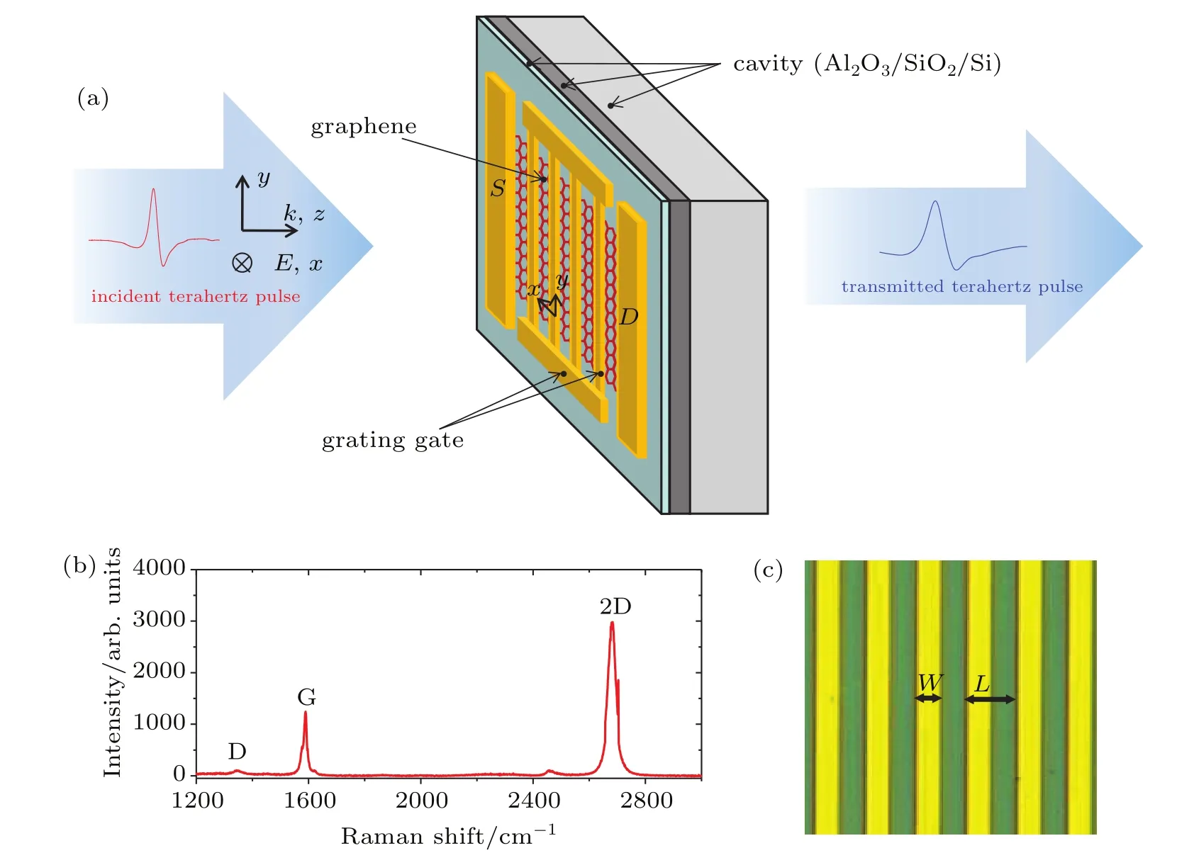
Fig.1.(color online)(a)Schematic structure of the device and the coordinate notation for transmission measurement. (b)Measured Raman spectrum of the transferred monolayer graphene on top of the Si/SiO2 substrate.(c)The optical photo of the grating gate.
3.Results and discussion
Transmission of the bare cavity and the grating-coupled graphene plasmon device are shown in Fig.2(a).The bare cavity is an insulator with constant transmission level in the THz region.However,the transmission spectra measured on the graphene device with resonant cavity shows that a prominent peak locates at 1.511 THz.This phenomenon implies that THz absorption is observably affected by graphene.Thus,extinction spectra(1−T/T0)for grating devices with VTG=−0.8 V, 0 V,0.8 V were then investigated.
To compare with the experimental data,we calculate (1−T/T0)of the graphene device theoretically by[11]
where T0and T are the transmissions passing through the bare cavity and the sample with the graphene,respectively.Z0is the vacuum impedance,and nsis the effective refractive index of the substrate.The solid curves in Fig.2(b)are fitting results according to Eq.(1)and the Lorentz conductivity.We use Lorentz conductivity for the graphene layer as[10,11]
where ω is the radian frequency of the incident terahertz light, n is the carrier density,and Γpis the plasmon resonance width. The resonance frequency is given by[10,11]

where ε and kGare effective dielectric constant and plasmon wave vector,respectively.The σuni=πe2/2h is the wellknown optical conductivity,and the Femi energy is given by EF=hvF(πn)1/2,vF=1×106m/s.If the sample is irradiated vertically by the light,the plasmon wave vector is determined by kG=mπ/W with m=1,2,3,...[11,17]
The corresponding solid curves in Fig.2(b)are fitting results according to Eqs.(1)–(3)with n and Γpas two fitting parameters.Three prominent features for the data are presented in Fig.2(b).First,the plasmon resonance width of the as prepared sample is approximately 3.5 THz,whereas the carrier density n ranges from 7.16×1012cm−2to 8.36×1012cm−2. Second,an obvious blue shift of the plasmon resonance frequency with decreasing top-gate voltage is observed:resonance frequencies are located at 1.523 THz,1.511 THz,and 1.506 THz for voltage of 0.8 V,0 V,and−0.8 V,respectively. Using a larger range of effective top-gate voltage,terahertz resonance in 1–2 THz can be straightforwardly achieved(see Fig.5).Third,the light–plasmon coupling in graphene is remarkably strong;transmission extinction at the plasmon resonance for VTG=0 V is more than 80%.A higher extinction can be achieved readily by enlarging the top-gate voltage VTG.

Fig.2.(color online)(a)Transmission spectra of the bare cavity(T0) and the device with graphene(T).(b)Extinction in transmission, 1−T/T0,in the graphene plasmonic device as gate voltage V G are−0.8, 0,and 0.8.The solid lines are fitting curves.Inset shows partial enlarged details inside the red-dashed box.The maximal transmission extinction is approximately 85%.
The electrical properties of the engineered graphene plasmon device are discussed by performing a fullest direct current(DC)measurement.Figure 3 shows the equivalent current model in the DC measurement.First,the output character is measured to obtain the device resistance(see Figs.3(a)and 4(a)).The channel current of the graphene device is found to be linear with the output voltage VDS,and the output resistance is proved to be a constant of 1639 Ω.Second,the leakage character of the fabricated graphene plasmon device is obtained in Figs.3(b)and 4(b).In the measurement,the source and drain electrodes are linked to the ground.Figure 3(b)shows the leakage measurement equivalent model. The top-gate structure can be regarded as a parallel between the top-gate capacitance Cxand junction resistance RGbecause of the top-gate leakage.In DC measurement,the current can only flow through the resistance RG.The leakage current results IG1and IG2show an almost perfect symmetry to the origin of coordinates(Fig.4(b)).The total leakage current is IG=IG1+IG2≈1.5µA when VTG=0.85 V.Thus,the junction resistance RGis approximately 0.6 MΩ,far less than that of small-size top-gate media.Meanwhile,the value of IG1is almost the same as that of IG2.Assuming two graphene channel resistances close to the source and drain electrodes are equal,RS≈RD.
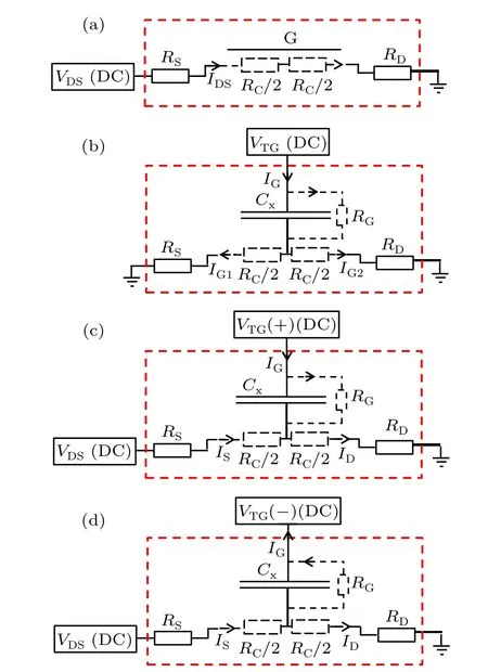
Fig.3.(color online)Equivalent current models.Here,R S and R D are considered as contact resistances in the source and drain electrodes,respectively.Graphene channel resistance is regarded as two parts close to the source and drain electrodes.Both resistances are set equally to calculate easily,and C x and R G are the top-gate capacitance and resistance,respectively.(a)Output-character measurement model.(b)Leak current measurement model.Panels(c)and(d)are transfer-characters measurements for positive and negative voltage,respectively.
Third,our double DC measurement of the prepared graphene device for different top-gate voltages will explicitly indicate the transfer character,as shown in Figs.3(c), 3(d),and 4(c).From the values of ID,IS,and IGextracted from the DC measurement(inset in Fig.4(c)),the actual topgate voltage VGset on the capacitance Cxat different gate voltages can be obtained in Fig.4(c).Here,VG=VTG−V (see Figs.3(c)and 3(d)),with graphene channel voltage V= ID(RD+RC/2)=VDS−IS(RS+RC/2).To further simplify, RS+RC/2=RD+RC/2=VDS/(IS+ID),V=VDSID/(IS+ ID).As a result,VG=VTG−VDSID/(IS+ID),and the actual channel current due to the graphene carrier can be expressed by IDS=V0/Rt,where the whole device resistance Rtcan be given by Rt=RD+RS+RC=2VDS/(IS+ID),and V0is set as 10 mV.The theoretical fitting for our transfer characteristic data will be discussed below.The carrier concentration(electrons or holes)in the graphene channel regions n related to the residual carrier concentration n0and the Diracpoint voltage VDiraccan be approximatedwhere Cxand n0can be set as 122.4 nF/cm2and 1×1012cm−2in our fitting model,respectively.The total device resistance Rtis given by Rt=Rcontact+L/(Weµn),[18]where the contact resistance is Rcontact=RS+RDand µ represents the mobility.Finally, the channel current is given by IDS=V0/Rt.The measured IDSagainst VG(symbols)along with the fitting results(solid lines)is shown in Fig.4(c).Then,the relevant parameters can be extracted:VDirac=−10.5 V,µ=1500 cm2·V−1·s−1and Rcontact=770 Ω.
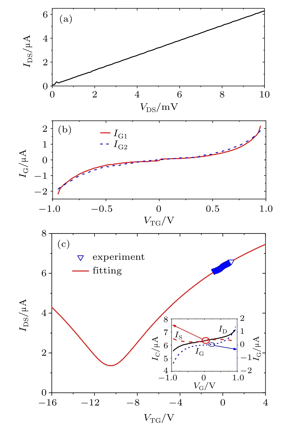
Fig.4.(color online)(a)Output characteristic curve.(b)Leak current curve(red solid line(I G1)and blue dashed line(I G2)).(c)Transfer characteristic curve of experimental and theoretical fitting results.Inset shows the channel and leakage results measured at the same time.
However,the variation range of the graphene plasmon frequency is very small,as shown in Fig.5.The calculating parameters were set as the same as those in Fig.4(c).In our experiments,tiny top-gate voltage range was applied to the device.Otherwise,when the larger top-gate voltage is applied to modulate the carrier density of the graphene channel,the leakage current can reach up more than 1.5µA(see Fig.4(b)). Therefore,the top-gate voltage can only be set as small as possible to avoid the large leakage current to breakdown the topgate capacitance.Two aspects should be considered to develop a device with a larger plasmon frequency range.First,defects of the top-gate media can be decreased by enlarging the growth temperature of ALDand applying the graphene prepared using molecular beam epitaxy(MBE).[19]As a result,the sustaining capability of the top-gate media can be improved directly.Second,the thickness and permittivity of top-gate dielectric layers can be optimized to enlarge its capacitance.Consequently,the range of graphene plasmon frequency can also be expanded (see the inset of Fig.5).
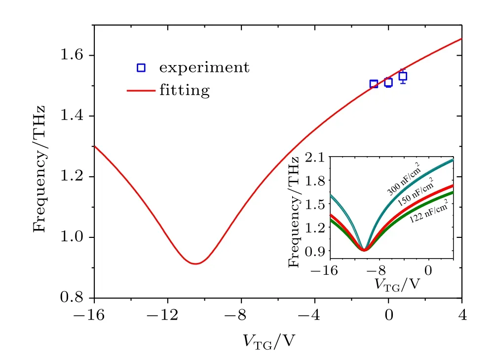
Fig.5.(color online)Experiment and theoretical frequency character of the prepared graphene plasmon device as a function of the top-gate voltage.Inset shows the graphene plasmon frequencies calculated at different top-gate dielectric capacitances.
4.Conclusion and perspectives
In summary,a tunable graphene plasmon device was fabricated with an Al2O3gate dielectric on its surface by ALD. A strong interaction between the graphene and the incident terahertz wave was expected because of the grating coupler and resonant cavity.The calculated results,including Lorentz conductivity of graphene,agree very well with our experimental results,and the extracted extinction value of the transmission in the resonance frequency is more than 80%at room temperature.Our DC measurement data revealed that a limited frequency range of the graphene plasmon was modulated. A superior graphene plasmon device with a larger frequency variable range may find applications in THz modulators by replacing the top-gate media with stronger sustaining ability and higher gate dielectric capacitance.
[1]Chen H T,Padilla W J,Zide Joshua M O,Gossard A C,Taylor A J and Averitt R D 2006 Nature 444 597
[2]Yen T J,Padilla W J,Fang N,Vier D C,Smith D R,Pendry J B,Basov D N and Zhang X 2004 Science 303 1494
[3]Wu H Q,Linghu C Y,Lu H M and Qian H 2013 Chin.Phys.B 22 098106
[4]Ryzhii V 2006 Jpn.J.Appl.Phys.45 923
[5]Hwang E H and Sarma S D 2007 Phys.Rev.B 75 205418
[6]Yan B,Yang X X,Fang J Y,Huang Y D,Qin H and Qin S Q 2015 Chin. Phys.B 24 015203
[7]Marinko J and Hrvoje B 2009 Phys.Rev.B 80 245435
[8]Ryzhii V,Satou A and Otsuji T 2007 J.Appl.Phys.101 024509
[9]Grigorenko A N,Polini M and Novoselov K S 2012 Nat.Photonics 6 749
[10]Vicarelli L,Vitiello M S,Coquillat D,Lombardo A,Ferrari A C,Knap W,Polini M,Pellegrini V and Tredicucci A 2012 Nat.Mater.11 865
[11]Yan B,Fang J Y,Qin S Q,Liu Y T,Zhou Y Q,Li R B and Zhang X A 2015 Appl.Phys.Lett.107 191905
[12]Marco F,Alexander U,Andreas P,Govinda L,Karl U,Hermann D, Pavel K,Aaron M,Werner S,Gottfried S and Thomas M 2012 Nano Lett.12 2773
[13]Nicolas U,Iris C,Julien L,Ievgeniia O N,Felix F,Michl K,Thomas S and Alexey B K 2013 Opt.Express 21 24736
[14]Ferrari A C,Meyer J C,Scardaci V,Casiraghi C,Lazzeri M,Mauri F, Piscanec S,Jiang D,Novoselov K S,Roth S and Geim A K 2006 Phys. Rev.Lett.97 187401
[15]Tu Z Q,Liu Z C,Li Y F,Yang F,Zhang L Q,Zhao Z,Xu C M,Wu S F,Liu H W,Yang H T and Richard P 2014 Carbon 73 252
[16]Lee B,Park S Y,Kim H C,Cho K,Vogel E M,Kim M J,Wallace R M and Kim J 2008 Appl.Phys.Lett.92 203102
[17]Zhu X L,Yan W Jepsen P U,Hansen O,Mortensen N A Xiao S S, Jackson R and Graham S 2013 Appl.Phys.Lett.102 131101
[18]Kim S,Nah J,Jo I,Shahrjerdi D,Colombo L,Yao Z,Tutuc E and Banerjee S K 2009 Appl.Phys.Lett.94 062107
[19]Sambonsuge S,Jiao S,Nagasawa H,Fukidome H,Filimonov S N and Suemitsu M 2016 Diam.Relat.Mater.67 51
17 April 2017;revised manuscript
10 June 2017;published online 27 July 2017)
10.1088/1674-1056/26/9/097802
∗Project supported by the National Natural Science Foundation of China(Grant No.11272337),the Research Project of National University of Defense Technology,China(Grant No.ZK16-03-34),the Natural Science Foundation of Hunan Province,China(Grant No.2016JJ3021),and the Open Project of Key Laboratory of Nanodevices and Applications,Suzhou Institute of Nano-tech and Nano-bionics,Chinese Academy of Sciences(Grant No.15ZS03).
†Corresponding author.E-mail:fjynudt@aliyun.com
©2017 Chinese Physical Society and IOP Publishing Ltd http://iopscience.iop.org/cpb http://cpb.iphy.ac.cn
猜你喜欢
广西文学(2022年1期)2022-10-20
湖南农业大学学报(自然科学版)(2022年3期)2022-07-19
上海人大月刊(2022年4期)2022-04-14
Chinese Physics B(2022年3期)2022-03-12
电影文学(2021年2期)2021-11-13
东方女性(2017年11期)2017-12-04
金秋(2017年10期)2017-08-31
青春岁月(2016年22期)2016-12-23
故事会(2016年8期)2016-05-06

- Chinese Physics B的其它文章
- Improved control for distributed parameter systems with time-dependent spatial domains utilizing mobile sensor actuator networks∗
- Geometry and thermodynamics of smeared Reissner–Nordström black holes in d-dimensional AdS spacetime
- Stochastic responses of tumor immune system with periodic treatment∗
- Invariants-based shortcuts for fast generating Greenberger-Horne-Zeilinger state among three superconducting qubits∗
- Cancelable remote quantum fingerprint templates protection scheme∗
- A high-fidelity memory scheme for quantum data buses∗