
Combined Effects of the Hole and Twin Boundary on the Deformation of Ag Nanowires: a Molecular Dynamics Simulation Study
2018-01-10 01:22WANGXiuXiuZHAOJianWeiYUGang
物理化学学报 2017年9期
WANG Xiu-Xiu ZHAO Jian-Wei YU Gang,*
Combined Effects of the Hole and Twin Boundary on the Deformation of Ag Nanowires: a Molecular Dynamics Simulation Study
WANG Xiu-Xiu1ZHAO Jian-Wei2YU Gang1,*
(1;2)
Based on molecular dynamics simulations, the plastic deformation of silver nanowires under uniaxial tension has been studied systematically. In this paper, the mechanical properties of [111]-oriented twin nanowires with different hole sizes have been studied. The existence of holes has no effect on the elastic deformation stage. The hole on the twin boundary has two main roles in the plastic deformation stage. During the initial stages of plastic deformation, the main function of the hole is to produce new dislocations as dislocation sources at small hole sizes. Upon increasing the hole size, the main effect changes to stop dislocation slip. During the late stages of plastic deformation, the two functions of the hole complement each other, upon increasing the hole size, the function of the hole as dislocation sources becomes obvious, leading to weakening of the plasticity of the nanowires.
Hole defect; Twin boundary; Tension; Silver nanowire; Molecular dynamics
1 Introduction
Metallic nanowires have been synthesized widely owing to their great potential applications in optical science, optical engineering mechanics, electronics and material science, etc1–4. Due to the effect of large surface-to-volume ratios, the structure and properties of nanowires are quite different from those of bulk materials5–8. Investigation of the mechanical behaviors of metal materials can provide the important insights and information to understand the nature of the nanowires and further promote the operation and improve the function of the nanodevices. Considerable studies on experimental measurements and computational simulations of understanding the mechanical properties of metallic nanowires under external loadings have been carried out9–14. Among these studies, it can be concluded that the deformations and strength of metallic nanowires are influenced by many factors, such as twin boundary (TB), defects, surface morphology, strain rate and temperature.
The TB is a kind of planar stacking faults whose lattice structures exhibit mirror symmetry across the boundary. It has always been of particular interesting because of the role as it plays in deformation processes15–18. In particular, as the critical dimensions of the material reduced to nanoscale, with the increase of the percentage of atoms located at or near the interfaces, the influence of the TBs becomes obvious. For example, many recent investigations in the metallic nanowires are associated with atomic-level mechanisms of plastic deformation at TBs19–24. Previous experiments have shown that the presence of high-density twins in copper nanowires can dramatically enhance the mechanical strength to present the considerable tensile ductility25–28. Compared to the experiments, molecular dynamics (MD) simulations have also been carried to understand the TB-strengthening21,23,29–33. Cao34have investigated the deformation mechanisms of twinned copper nanowires with a square cross-section using the MD simulation. They reported that the smaller TB spacing, the higher yielding stresses of the twinned nanowires. Deng and Sansoz35proposed a similar simulation models compared to the Cao’s work and predicted the linear dependence of yield stress as a function of number of TBs per unit length in periodically twinned Au nanowires with different diameters. Guo and Xia30established an analytical model based on kinetic rate theory to discuss the above-mentioned competing mechanisms. Moreover, Deng and Sansoz36further took the temperature effect into the study and put forward rate-controlling deformation mechanisms to show the surface dislocation emission and twin-slip interaction. All these studies of TB-strengthening demonstrated twin boundary spacing governs the mechanical properties and deformation behaviors of twinned metallic nanowires.
On the other hand, defects also play an important role in the generation of dislocation, slips or stacking faults. It is demonstrated that the existences of defects destroy the integrity of material structure, and it will lead to the serious influence on the physical properties of nanomaterials37,38. Meyers and Aimone39have observed the dislocation growth near the hole in the experiment of rapid compression of copper grain, copper holes emit a lot of slip bands near grain boundary, but due to the limitation of experimental technology, accurate dislocation and the dynamic process are difficult to acquire. Therefore, molecular dynamics calculation is essentially important for the comprehensive understanding of the defects effect in the microscopic material mechanics40,41. Deng and Sansoz36discovered that special defects could be utilized to approach a near-ideal strength in gold nanowires through microstructural design. Silva42studied the formation, evolution and breaking of gold nanowires, and they showed how defects led to the formation of one-atom constrictions in the gold nanowires.
Although much progress has been made on the experiment and theoretical calculation, there are rare reports on the direct study combined twin boundary and hole. Therefore, it is worth to study how the combined effects of the hole and twin boundary on the deformation of nanowires. In this work, we designed and constructed the silver nanowires with specific structures. By means of MD simulation, we will present their influence on the TB-strengthening and the deformation mechanism of silver nanowires.
2 Simulation method
Cuboid samples with the dimensions of 9.45 nm × 9.45 nm × 22.09 nm and~0.09 million atoms were constructed using a Voronoi tessellation construction as a matrix, as shown in Fig.1. The models of silver samples containing a twin boundary and a hole where on the twin boundary, and the hole is on the twin boundary. Three typical twinned nanowires with holes are illustrated in the figures, while one twinned nanowire with no hole (specimen I) is presented for comparison. The hole radius () of the second, third and fourth wires are 0.33 nm (0.8 lattices) (specimen II),0.82 nm (2.0 lattices) (specimen III) and 2.45 nm (6.0 lattices) (specimen IV), respectively. MD simulations were performed on the polycrystalline silvers with different length-diameter ratios using a self-developed software NanoMD43–47. A constant strain rate of 1.09 × 10⁹s−1was used in all simulations. The embedded atom method (EAM) potential48–50was adopted to analyze the atomic interaction of Face Centered Cubic (FCC) silver atoms. Free boundary conditions were applied in all three spatial dimensions to model a columnar-like structure. Prior to any imposed stress, each sample was equilibrated at a constant temperature for 51.3 ps to relax the unfavorable configurations in the grain boundaries. After reaching a steady-state arrangement, change the hole radius to extract temperature-dependent behaviors of the simulations.
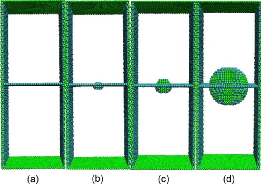
Fig.1 Atomistic model of [111] silver nanowires.
(a) specimen I, (b) specimen II, (c) specimen III, (d) specimen IV.
In order to study the structures of plastically deformed polycrystralline nanowires in detail, different types of defects are identified by means of the centro-symmetry parameter51. The centro-symmetry parameter can be defined as:

(1)
where RandR+6are the vectors corresponding to the six pairs of opposite nearest neighbours in the FCC lattice,0is the distance of the nearest neighbours andpis the centro-symmetry parameter value of atomin the lattice. For reference, p< 0.4 corresponds to the FCC structure, especiallyp= 0 reflects a perfect silver lattice. 0.7 <p< 1.2 stands for stacking faults, corresponding to the hexagonal close-packed (HCP) atoms. 1.2 <p< 1.8 represents for atoms halfway between HCP and the surface atoms, andp> 1.8 is equivalent to surface atoms. For convenience,p> 1.2 is regarded as other atoms for discussion in the following paragraphs.
The stress within the nanowires is computed by the virial scheme, and the overall stress is taken as the average of all atomistic stresses52. The corresponding atomic stress is expressed in terms of embedded-atom method potential functions as follows:
(2)
whereis thecomponent of the atomic stress tensor of atom,is its volume,is the mass andvis the velocity component in thedirection of atom,,,andare parameters from EAM potential. The first and second terms on the right side of the above-mentioned equation represent the thermal and atomic interactions, respectively.
3 Results and discussion
3.1 The influence of the hole size as studied with the potential energy and stress-strain curves
Potential energy is the stored energy of an object. It is the energy by virtue of an object’s. Generally, the potential energy is equal to the total energy divided by the total number of atoms in the system. Fig.2 shows the potential energy responses of seven nanowires at 10 K under tensile loading. In the elastic stage (the area <1> in Fig.2), elastic potential energyis the potential mechanical energy stored in the configuration of a material or physical system as work is performed to distort its volume or shape. After fitting, we observe that the potential energy increases in the form of a parabola (= 1/22). Theis 5.90 × 10⁻¹², 6.51 × 10⁻¹², 6.69 × 10⁻¹², 6.65 × 10⁻¹², 6.27 × 10⁻¹²and 6.35 × 10⁻¹²eV·strain−1, respectively. After many fitting, the error range ofis 3%–6%. From Fig.2, we can observe that the twinned nanowire without hole has least potential energy. At small hole size, the potential energy of the sample is lower than the single crystal nanowire, by raising hole size, the potential energy is higher than the single crystal nanowire.This is because the inner surface atoms of the hole can increase the potential energy. With the increase of the hole size, the hole effect on the potential energy is dominant. In the plastic stage, the potential energy has a slight decline, then, because of the large amounts of dislocation slips produced, the potential energy presents fluctuation. It is known that the potential drop is proportional to the sliding area. The TB can block the dislocation slip during the stretching, reducing the area. Therefore, the sample of single crystal needs biggest potential drop on dislocation slip. We also observe that the potential drop increases with the hole size increasing. This is because the larger hole releases more energy while the structure collapses during stretching.
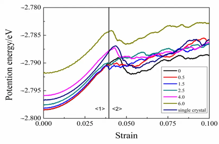
Fig.2 Potential energy curves for Ag nanowires at 10 K. color online.
Fig.3 plots the stress-strain curves of the ten nanowires at 10 K. Ten nanowires subjected to a tensile loading exhibit the features of both elastic and plastic deformations. It is observed that each curve increases up to a threshold stress, corresponding to the yield point. The yield stress of the single crystal nanowire is expected to exhibit a maximum yield stress, that is, about 20% larger than that of the twinned nanowires with a hole in spite of the hole size. After the yield point, the curves decrease with significant fluctuations until the final breaking.
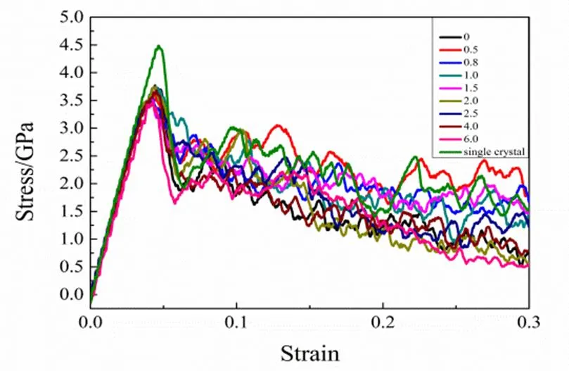
Fig.3 Stress-strain curves for the ten simulated Ag nanowires.color online.
To further reveal the influence of the hole on the deformation and breaking behaviors, we studied yield stress, yield strain, Young′s modulus and fracture strain as functions of the hole radius. Fig.4(a) shows the yield stress-hole radius curve. We can observe that the yield stress does not have significant change with the increase of the hole size, the average of the yield stress is about (3.67±0.08) GPa, less than that of single crystal. Similarly, the hole has no obvious effect on the yield strain as shown in Fig.4(b). The average value of the yield strain is about 0.045±0.006. In Fig.4(c), the average Young’s modulus has a first increase followed by a decrease with hole radius increasing, but the overall change is not obvious. Gao.53studied the silver nanowires with different twin boundary spacing, they found that twin boundary spacing has no effect on Young’s modulus. Gao also mentioned that the effect of hole size on silver nanowires is not significant in his Ph.D. thesis, which is consistent with our result. We know the Young’s modulus is defined as the stress of a material divided by its strain in the elastic deformation region, which may be used to evaluate the mechanical strength of the nanowires. So, from Fig.4((a)−(c)), we can observe that the hole effect on the twinned Ag nanowires is not obvious in elastic region. Fig.4(d) illustrates the fracture strain as function of the hole radius. We observed that with the increase of the hole radius, the fracture strain decreases. We can explain the decrease of the fracture strain from the generation of dislocations. Most dislocations are originated from surfaces, including the inter surface of the cavity. Therefore, the larger the inter surface may result in more dislocations. Then, the system more quickly reaches the necking position till final breaking, showing a smaller fracture strain. Meanwhile, the surface, including the inner surface, can block the propagation of the dislocation, the bigger the inner surface, the smaller the dislocation area, thus the fluctuation gets smaller.
3.2 Influence of the hole size as studied with the statistics of the specific atoms
To reveal the hole radius-dependence of plastic deformation samples, Fig.5 illustrates the evolution of the relative numbers of FCC, HCP and other atoms in the series of nanowires during the tensile loading. The relative number of the atoms is defined as the number at a certain strain subtracts the number before deformation. The positive value represents the increase, and. In the elastic deformation region with the strain from 0 to 3.0%, there is no significant change in the number of all atoms. After 3.0% strain, the nanowires get into the plastic deformation stage. The number of FCC atoms decreases accompanied with increasing HCP atoms. The sharp increase of HCP atoms in incipient plastic deformation indicates that the nucleation and motion of dislocation activities may be the dominant deformation mechanism for samples. The number of other atoms has a small increase in different time periods, as shown in Fig.5. The other atoms mainly represent the atoms in low centrosymmetry environment, including the hole surface atoms. In the late stage of plastic deformation (after 0.045 strain), the reduction of FCC atoms is not completely converted to HCP atoms, but also leads to the increase of the other atoms. It indicates that the mechanism transition in the late stage of plastic deformation.
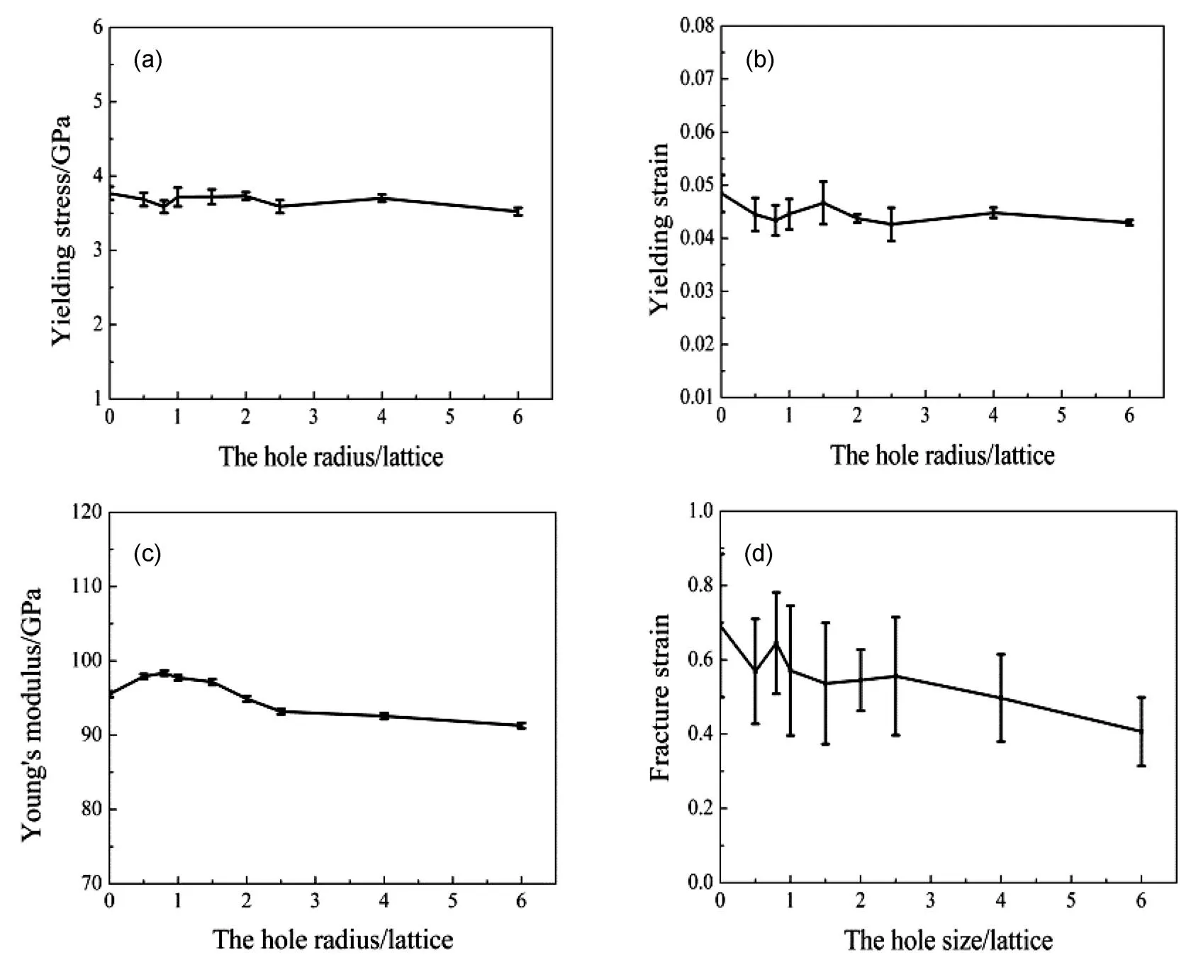
Fig.4 Mechanical properties of Ag nanowires with different hole size.
(a) the yielding stress, (b) the yielding strain, (c) Young’s modulus and (d) fracture strain of the nanowire plotted against the hole size, respectively.

Fig.5 Reduce number of different atoms versus strain of [111] elongation.
(a) specimen I; (b) specimen II; (c) specimen III; (d) specimen IV.
Generally, the change of the number of HCP atoms shows the generation of dislocations. In order to further investigate the hole effects, we draw the variation speed of the number of HCP atoms with hole surface area curve as shown in Fig.6. From Fig.6, we can observe that when the hole radius is less than 2.5 lattices, the variation speed of the number of HCP atoms increases with the hole surface area increasing. In contrast, when the hole size is more than 2.5 lattices, the variation speed of the number of HCP atoms decreases with the hole surface area increasing. We can infer that when the hole radius is less than 2.5 lattices, with the increase of the hole, more dislocations are generated from hole surface, so the faster the number of HCP atoms increased. Interestingly, the rate increases linearly with the increase of the hole surface area. But hole radius to a certain extent, because of the function which the hole can blocks dislocation slips, the slip plane area gets smaller, thus, the speed of the number of HCP atoms decreases.
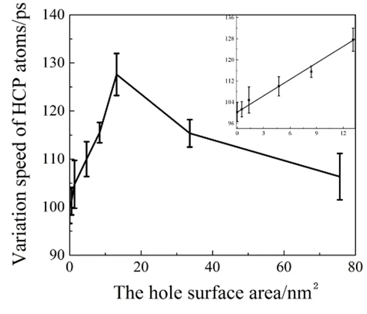
Fig.6 FCC atoms reduce rate with different hole surface area.
3.3 Influence of the hole size as studied with the atomic configuration
To further study how the hole affects the plastic deformation of the nanowire, we have captured the microstructure evolution of specimens I, II, III and IV, respectively. The microstructure evolution of specimens I and III are shown in Figs.1 and 2 in supplementary material.
Figs.7 and 8 show the dislocation evolution in specimens II and IV at yield point and the following picoseconds. Figs.7(a) and 8(a) correspond to the true yield point. At true yield point, the initial dislocations are all emitted from the surface in specimens II and IV (the letter “A” in Figs.7(a) and 8(a)) and it is not affected by the hole, in accordance with the result of the first stage which the hole has no effect on the initial dislocation generated in Fig.5. Figs.7(b, c), and 8(b, c) correspond to the yield point and the first release point, respectively. From the microscopic point of view, it is explained that with the increase of hole radius, the change rate of HCP atomic number increases first and then decreases. Compared with specimen IV, the main hole of specimens II, III is as dislocation sources generate new dislocations (the letter “B” in Figs.7(b) and 8(b)). While the main role of the hole of specimen IV blocks the dislocation slips, and the dislocation generated rate is lower than specimens I, II, III corresponding to Fig.6. In Figs.7(c) and 8(c), a large number of dislocations are generated and partial dislocations are absorbed by twin boundary or the front dislocation. In Fig.8(c), the hole in twin boundary has two roles, one generates new dislocations as dislocation sources, and the other blocks the dislocation slip. Figs.7(d) and 8(d) corresponds to the strain is 0.1, where the number of HCP atoms appears fluctuation. In Figs.7(d) and 8(d), the continuous generation and disappearance of the dislocations result in the number of HCP atoms appearing fluctuation. Figs.7(e) and 8(e) corresponds to the point where the necking appears. In Fig.7(e), the necking appears at the 1/2 of the nanowire when it deforms to 26%. The necking of specimen IV appears at the hole surface when the nanowire deforms to 15% in Fig.8(e). Combining Figs.4(d) and 5, we can observe that the larger the hole, the easier the necking appears and the easier the nanowires break.

Fig.7 Tensile yielding of specimen II at 10 K.
(a) the generation of the initial dislocation specimen II before yield point. (b) atomic structure of the deformed sample at= 4.1%. (c) atomic structure of the deformed sample at= 6.2%. (d) atomic structure of the deformed sample at= 10.0%. (e) atomic structure of the deformed sample at= 26.0%.

Fig.8 Tensile yielding of specimen IV at 10 K.
(a) the generation of the initial dislocation specimen IV before yield point. (b) atomic structure of the deformed sample at= 4.2%. (c) atomic structure of the deformed sample at= 5.7%. (d) atomic structure of the deformed sample at= 10.0%. (e) atomic structure of the deformed sample at= 15.0%.
Conclusively, the hole has no effect on the elastic deformation of twin silver nanowires. The hole effect is mainly manifested in the plastic deformation stage. There are two main functions, one is to block the dislocation slips, the other is to generate new dislocations as dislocation sources. In the initial plastic deformation, the main function of the hole is to generate new dislocations as dislocation sources at small hole size. By raising the hole size, the main function of the hole is to block dislocation slip. In the late stage of plastic deformation, the two functions of the hole complement each other, with the hole size increasing, the function of the hole surface atoms as dislocation sources becomes more significant, leading to the plastic of nanowires weaken.
4 Conclusions
In this work, we performed a MD simulations on the tensile deformation behavior of twinned nanowires with different hole size at 10 K. It was found that the potential energy is higher than the single crystal nanowire when the hole radius is greater than 1.64 nm, in contrast, the potential energy is lower than the single crystal nanowire. We also found that the initial dislocations are all emitted from the surface and the hole has no effect on the initial dislocation generated. However, in this work, the main finding is that the hole on the twin boundary has two main functions in the plastic deformation stage. In the initial stage of plastic deformation, generating new dislocations as dislocation sources is the main function of the hole at small hole size. By raising the hole size, the main function of the hole is to block dislocation slip. In the late stage of plastic deformation, the two functions of the hole complement each other, with the hole size increasing, the function of the hole surface atoms as dislocation sources becomes more significant, leading to the plastic of nanowires weaken.
Supporting Information: available free of chargethe internet at http://www.whxb.pku.edu.cn.
(1) Wan, Q.; Li, Q. H.; Chen, Y. J.; Wang, T. H.; He, X. L.; Li, J. P.; Lin, C. L.... 2004,, 3654. doi: 10.1063/1.1738932
(2) Liu, H. Q.; Kameoka, J.; Czaplewski, D. A.; Craighead, H. G.. 2004,, 671. doi: 10.1021/nl049826f
(3) Melosh, N. A.; Boukai, A.; Diana, F.; Gerardot, B.; Badolato, A.; Petroff, P. M.; Heath, J. R.2003,, 112. doi: 10.1126/science.1081940
(4)Husain, A.; Hone, J.; Postma, H. W. C.; Huang, X. M. H.; Drake, T.; Barbic, M.; Scherer, A.; Roukes, M. L.2003,, 1240. doi: 10.1063/1.1601311
(5) Park, H. S.; Cai, W.; Espinosa, H. D.; Huang, H. C.2009, 34, 178. doi: 10.1557/mrs2009.49
(6) Lieber, C. M.; Wang, Z. L.2007,, 99. doi: 10.1557/mrs2007.41
(7) Alexandrov, A. S.; Kabanov, V. V.2005,, 076601. doi: 10.1103/PhysRevLett.95.076601
(8) Xia, Y. N.; Yang, P. D.; Sun, Y. G.; Wu, Y. Y.; Mayers, B.; Gates, B.; Yin, Y. D.; Kim, F.; Yan, Y. Q.. 2003,, 353. doi: 10.1002/chin.200322236
(9) Liang, H. Y.; Upmanyu, M.; Huang, H. C...2005,, 241403. doi: 10.1103/ PhysRevB.71.241403
(10) Diao, J.; Gall, K.; Dunn, M. L....2004,, 1935. doi: 10.1016/j.jmps.2004.03.009
(11) Rodrigues, V.; Fuhrer, T.; Ugarte, D.... 2000,, 4124. doi: 10.1103/PhysRevLett.85.4124
(12) Rego, L. G. C.; Rocha, A. R.; Rodrigues, V.; Ugarte, D...2002,, 106. doi: 10.1103/ PhysRevB.67.045412
(13) Kondo, Y.; Takayanagi, K.... 1997,, 3455. doi: 10.1103/PhysRevLett.79.3455
(14) Wen, Y. H.; Zhang, Y.; Wang, Q.; Zheng, J. C.; Zhu, Z. Z.... 2010,, 513. doi: 10.1016/j.commatsci.2010.02.015
(15) Algra, R. E.; Verheijen, M. A.; Borgstrom, M. T.; Feiner, L. F.; Immink, G.; Enckevort, W. J. P.; Vlieg, E.; Bakkers, E. P. A. M.2008,, 369. doi: 10.1038/nature07570
(16) Johansson, J.; Karlsson, L. S.; Svensson, C. P. T.; Martensson, T.; Wacaser, B. A.; Deppert, K.; Samuelson, L.; Seifert, W... 2006,, 574. doi: 10.1038/nmat1677
(17) Wang, D. H.; Wang, D. Q.; Hao, Y. J.; Jin, G. Q.; Guo, X. Y.; Tu, K. N.2008,, 215602. doi: 10.1088/0957-4484/19/21/215602
(18) Shim, H. W.; Zhang, Y.; Huang, H.... 2008,, 10257. doi: 10.1063/1.2979716
(19) Sansoz, F.; Deng, C.... 2008,, 086101. doi: 10.1063/1.2970029
(20) Wu, B.; Heidelberg, A.; Boland, J. J.; Sader, J. E.; Sun, X. M.; Li, Y. D.. 2006,, 468. doi: 10.1021/nl052427f
(21) Sangid, M. D.; Ezaz, T.; Sehitoglu, H.. 2011,, 283. doi: 10.1016/j.actamat.2010.09.032
(22) Bernardi, M.; Raja, S. N.; Lim, S. K.2010,, 285607. doi: 10.1088/0957-4484/21/28/285607
(23) Wen, Y. H.; Huang, R.; Zhu, Z. Z.; Wang, Q.... 2012,, 205. doi: 10.1016/j.commatsci.2011.11.020
(24) Zhang, J. J.; Xu, F. D.; Yan, Y. D.; Sun, T.... 2013,, 684. doi: 10.1007/s11434-012-5575-3
(25) Lu, K.; Lu, L.; Suresh, S.2009,, 349. doi: 10.1126/science.1159610
(26) Lu, L.; Sui, M. L.; Lu, K.. 2000,, 1463. doi: 10.1126/science.287.5457.1463
(27) Lu, L.; Chen, X.; Huang, X.; Lu, K.2009,, 607. doi: 10.1126/science.1167641
(28) Lu, L.; Shen, Y. F.; Chen, X. H.; Qian, L. H.; Lu, K2004,, 422. doi: 10.1126/science.1092905
(29) McDowell, M. T.; Leach, A. M.; Gaill, K... 2008,, 3613. doi: 10.1021/nl801526c
(30) Guo, X.; Xia, Y. Z.. 2011,, 2350. doi: 10.1016/j.actamat.2010.06.047
(31) Kulkarni, Y.; Asaro, R. J.. 2009,, 4835. doi: 10.1016/j.actamat.2009.12.031
(32) Zhang, Y. F.; Huang, H. C.; Atluri, S. N.... 2008,, 215. doi: 10.3970/cmes.2008.035.215
(33) Ding, F.; Li, H.; Wang, J. L.; Shen, W. F.; Wang, G. H..... 2002,, 113. doi: 10.1088/0953-8984/14/1/310
(34) Cao, A. J.; Wei, Y. G.; Mao, S. X.... 2007,, 151909. doi: 10.1063/1.2721367
(35) Deng, C.; Sansoz, F.2009,, 1517. doi: 10.1021/nl803553b
(36) Deng, C.; Sansoz, F.2009,, 3001. doi: 10.1021/nn900668p
(37) Wu, H. A.; Liu, G. R.; Wang, J. S.2004,, 225. doi: 10.1088/0965-0393/12/2/004
(38) Heino, P.; Hakkinen, H.; Kaski, K.1998,, 641. doi: 10.1103/PhysRevB.58.641
(39) Meyers, M. A.; Aimone, C. T.1983,, 1. doi: 10.1016/0079-6425(83)90003-8
(40) Kohlhoff, S.; Gumbsch, P.; Fischmeister, H. F.1991,, 851. doi: 10.1080/01418619108213953
(41) Fischmeister, H. F.; Exner, H. E.; Poech, M.H.; Kohlhoff, S.; Gumbsch, P.; Schmauder, S.; Sigl, L. S.; Spiegler, R.1989,, 839.
(42) Silva, E. Z.; Novaes, F. D.; Silva, A. J. R.; Fazzio, A.2004,, 115411. doi: 10.1103/PhysRevB.69.115411
(43) Zhao, J. W.; Yin, X.; Liang, S.; Liu, Y. H.; Wang, D. X.; Deng, S. Y.; Hou, J..... 2008,, 367. doi: 10.1016/S1005-9040(08)60077-X
(44) Wang, D. X.; Zhao, J. W.; Hu, S.; Yin, X.; Liang, S.; Liu, Y. H.; Deng, S. Y.. 2007,, 1208. doi: 10.1021/nl0629512
(45) Liu, Y. H.; Zhao, J. W.; Wang, F. Y...2009,,
115417. doi: 10.1103//PhysRevB.80.115417
(46) Wang, F. Y.; Gao, Y. J.; Zhu, T. M.; Zhao, J. W.2011,, 1624. doi: 10.1039/CONR00797H
(47) Liu, Y. H.; Wang, F. Y.; Zhao, J. W.; Jiang, L. Y.; Kiguchi, M.; Murakoshi, K..... 2009,, 6514. doi: 10.1039/B902795E
(48) Johnson, R. A...1988,, 3924. doi: 10.1103/PhysRevB.37.3924
(49) Johnson, R. A...1988,, 6121. doi: 10.1103/PhysRevB.37.6121
(50) Johnson, R. A...1989,, 12554. doi: 10.1103/PhysRevB.39.12554.
(51) Kelchner, C. L.; Plimpton, S. J.; Hamilton, J. C...1998,, 11085. doi: 10.1103/PhysRevB.58.11085.
(52) Wu, H. A.2006,, 370. doi: 10.1016/j.euromechsol.2005.11.008
(53) Gao, Y. J.; Sun, Y. L.; Yang, X. B.; Sun, Q.; Zhao, J. W.;2015,, 1546. doi: 10.1080/08927022.2014.999238
孔洞和孪晶界对银纳米线形变行为联合影响的分子动力学模拟
汪秀秀1赵健伟2,*余 刚1,*
(1湖南大学化学生物传感与计量学国家重点实验室,化学化工学院,长沙 410082;2嘉兴学院材料与纺织工程学院,浙江 嘉兴 314001)
在分子动力学模拟的基础上,系统地研究了银纳米线在单轴拉伸条件下的塑性形变。本文研究了不同孔径大小的[111]晶向的孪晶纳米线的力学性能。研究发现,孔洞的存在对弹性形变阶段没有影响。孪晶界上的孔洞在塑性形变阶段主要有两个作用。在初始塑性形变阶段,当孔洞的尺寸较小时,主要是作为位错源产生新的位错;随着孔洞尺寸的增大,主要作用变为阻碍位错滑移。在塑性形变的后期,孔洞的两个作用相辅相成,但随着孔洞尺寸的增大,孔洞作为位错源产生位错的作用变得显著,最终导致纳米线的塑性减弱。
孔洞缺陷;孪晶界;拉伸;银纳米线;分子动力学
O641
10.3866/PKU.WHXB201705087
March 16, 2017;
April 27, 2017;
May 8, 2017.
YU Gang, Email: yuganghnu@163.com; Tel: +86-1897493643. ZHAO Jian-Wei, Email: zhaojw@nju.edu.cn; Tel: +86-13967321774.
The project was supported by the National Natural Science Foundation of China (51271074).
国家自然科学基金(51271074)资助
猜你喜欢
老年教育(老年大学)(2022年8期)2022-08-24
西南科技大学学报(2021年4期)2022-01-15
电子技术与软件工程(2021年7期)2021-06-16
收藏界(2019年3期)2019-10-10
学生天地(2019年30期)2019-08-25
人工晶体学报(2019年7期)2019-08-22
中学数学杂志(初中版)(2017年4期)2017-08-28
无机盐工业(2017年7期)2017-03-10
爆炸与冲击(2016年5期)2016-04-17
西华大学学报(自然科学版)(2015年3期)2015-07-18

- 物理化学学报的其它文章
- Development and Validation of a Reduced Chemical Kinetic Mechanism for HCCI Engine of Biodiesel Surrogate
- Cobalt@cobalt Carbide Supported on Nitrogen and Sulfur Co-Doped Carbon: an Efficient Non-Precious Metal Electrocatalyst for Oxygen Reduction Reaction
- OL负载Cu催化剂及其催化氧化CO及乙酸乙酯性能
- Efficient Synthesis of Sulfur and Nitrogen Co-Doped Porous Carbon by Microwave-Assisted Pyrolysis of Ionic Liquid
- First-Principles Study: the Structural Stability and Sulfur Anion Redox of Li1−xNiO2−ySy
- S掺杂促进Fe/N/C催化剂氧还原活性的实验与理论研究