
Monolithic semi-polar(1¯101)InGaN/GaN near white light-emitting diodes on micro-striped Si(100)substrate∗
2019-08-16 01:20QiWang王琦GuoDongYuan袁国栋WenQiangLiu刘文强ShuaiZhao赵帅LuZhang张璐ZhiQiangLiu刘志强JunXiWang王军喜andJinMinLi李晋闽
Chinese Physics B 2019年8期
Qi Wang(王琦), Guo-Dong Yuan(袁国栋),†, Wen-Qiang Liu(刘文强), Shuai Zhao(赵帅),Lu Zhang(张璐), Zhi-Qiang Liu(刘志强), Jun-Xi Wang(王军喜), and Jin-Min Li(李晋闽)
1Center for Semiconductor Lighting,Institute of Semiconductors,Chinese Academy of Sciences,State Key Laboratory of Solid State Lighting,Beijing Engineering Research Center for the 3rd Generation Semiconductor Materials and Application,Beijing 100083,China
2Center of Materials Science and Optoelectronics Engineering,University of Chinese Academy of Sciences,Beijing 100049,China
Keywords: InGaN/GaN MQWs,near white light-emitting diodes,Si(100)substrate
1. Introduction
Over the last few years,GaN-based light-emitting diodes(LEDs) have been rapidly developed due to their low energy consumption and long lifetime.[1-5]By reducing the indium content, the band gap of InGaN increases from 0.7 eV to 3.4 eV,which corresponds to the wavelength of emission from ultraviolet to infrared.[6-8]Traditionally, polar blue InGaN-based LEDs are combined with phosphors to produce white LEDs[9-12]This method has achieved a high lumen efficiency(197.8 lm/W),[13]but this method is not a fully meaningful LEDs lighting technology, and there are still some shortcomings: the process is complex,[14]conversion efficiency is still far from the theoretical efficiency limit(298.7 lm/W),[13]and polar InGaN has a strong quantum confined stark effect(QCSE).[15]As a result, researchers are looking for a new method to produce white LEDs on a monochromatic chip with no phosphors. For example,by growing a hexagonal nanopillar and inverted pyramid structure,the mixed structures of polar and semi-polar multiple quantum wells (MQWs), or inclined polar MQWs with changing the in-plane indium content in MQWs are prepared.[16-18]The white LEDs can also be achieved by changing the indium content of MQWs in polar,semi-polar and non-polar MQWs,respectively.[19-22]Nevertheless,the white LEDs have not been realized by changing the in-plane In content in semi-polar InGaN/GaN MQWs.The semi-polar facets of nitride include (1¯101), (11¯22), (20¯2¯1),etc., the first-principles calculation shows theoretically that the In incorporated in semi-polar facet is higher than in polar facet.[23,24]The semi-polar facet has a lower strain state than polar facet,which will give rise to higher In content[25,26]It was experimentally reported that the semi-polar(1¯101)has the maximum In content incorporation-efficiency compared with polar,nonpolar,and other semi-polar planes.[26]For long wavelength nitride LEDs, the InGaN/GaN MQWs with high indium content are needed, which is necessary for fabricating monochromatic white LEDs. The Si-based LEDs have become a hot research topic.[27-32]There are already some publications about semi-polar(1¯101)GaN grown on patterned Si(100)substrate.[33-37]Most of these studies focus on the growing of single-layer semi-polar GaN films, blue-green LEDs,blue lasers, and high-In content InGaN/GaN MQWs.[34,35]However,the white LEDs based on semi-polar(1¯101)MQWs on patterned Si (100) substrates have not yet been reported,which is probably due to V-grooves on a patterned Si (100)substrate with a width smaller than 3µm.[35]In such a small width,in-plane distribution of the indium content is more uniform and corresponding emission waveband is too narrow to emit wide spectrum light.Here in this work,semi-polar(1¯101)MQWs are grown on patterned Si (100) substrates with a V-groove width of ∼10µm. The wide in-plane indium distribution in semi-polar (1¯101) MQW is realized by carefully controlling the size of micro-stripe and the growth temperature of the InGaN, and the electroluminescence (EL) of white LEDs is reported.
2. Experiment
An InGaN MQW structure was grown on a(1¯101)plane GaN by selective-area epitaxy on inclined Si (111) planes etched from a Si(100)substrate as shown in Fig.1. First,the micro-stripes on Si(100)substrate were fabricated by depositing a 200-nm-thick silicon dioxide(SiO2)hard mask layer via plasma-enhanced chemical vapor deposition (Fig. 1(b)) followed by conventional photolithography (Fig. 1(c)), then the SiO2and photoresist were removed from the surface. After that, the Si(100)substrate was etched by tetramethyl ammonium hydroxide and isopropyl alcoholmixed solution, which is normally used for the anisotropic etching of(100)-oriented Si[38,39]as reported previously in our work.[40]Finally,the two opposite Si(111)planes were exposed with an inclined angle of about 54.7°with respect to the horizontal Si (100) plane.The LED structures were grown on a two-inch-thick p-type patterned Si (100) substrate by metal organic chemical vapor deposition(MOCVD).Trimethylgallium,trimethylaluminum,and ammonia were used as the Ga, Al, and N precursor, respectively. And hydrogen (H2) served as the carrier gas. As shown in Fig. 1(f), a 30-nm-thick AlN nucleation layer was deposited at 600°C and a 300-nm-thick AlN nucleation layer was deposited at 1100°C followed by a graded AlGaN buffer layer in which the Al content changed from 10% to 100%.Next, we deposited a 3-µm-thick n-GaN layer at 800°C, 11 periods of InGaN/GaN MQWs at 700°C/834°C, and a fiveperiod AlGaN/GaN superlattice.Finally,100-nm-thick p-GaN and 20-nm-thick u-GaN layer are grown as shown in Fig. 1.With a given sized patterned-Si (100) substrate, the growing of semi-polar(1¯101)LED structures shows a very good reproducibility.
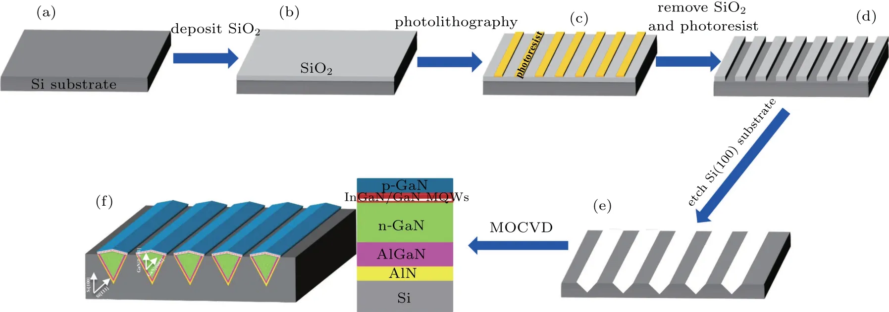
Fig. 1. Schematic diagram of (a) Si (100) substrate, (b) Si (100) substrate with SiO2 mask, (c) photolithography, (d) removing SiO2 and photoresist,(e)developing trenches by TMAH,(f)InGaN multiple-quantum-well system grown on the(1¯101)plane of GaN based on selectivearea epitaxial growth.
The morphology of the epitaxy structures was characterized by scanning electron microscopy (SEM). The structural analysis of the LED epitaxy structure formed on the micro-striped Si (100) substrate was performed by transmission electron microscopy (TEM). The cathodoluminescence(CL) measurements were conducted to determine the luminescence spectra. For functional testing, lateral LED devices were fabricated. A p-contact was deposited by electron-beam evaporation and defined by photolithography and lift-off. The Cr/Al/Ti/Au was used for the n-contact and the probing pad.The electroluminescence (EL) spectra of the LEDs indicate that the semi-polar InGaN/GaN MQWs emit near white light.
3. Results and discussion
From the cross-sectional SEM image in Fig.2(a),we obtain smooth triangular protrusions with Si(111)and(¯1¯11)side planes, and a period of 15µm, and 10-µm-wide trenches between the protrusions. Figure 2(b) shows an SEM image of the cross-section of the epilayers grown in the grooves shown in Fig.2(a). In our experiments,the size of the micro-stripe is enlarged:its maximum size is only 3µm in Ref.[35],whereas we use lithography to produce micro-stripes of 10µm or even larger V-groove to analyze the inner structures. The large size is favorable for the research of subsequent devices: the larger the more favorable. Besides,the width of the MQW is closely related to the size of the micro-stripe. Figure 2(c)reveals the surface morphology from a top-down view. The morphology is slightly roughened by the two opposite layers colliding with each other. The c (0001) plane of GaN completely disappears,and the semi-polar(1¯101)plane covers the whole stripe surface,which is shown in Fig.2(d). Figure 2(d)shows a cross-sectional SEM image of InGaN/GaN MQWs grown on a Si(111)plane,from which we see that the inclined angle between the side wall and the flat is ∼7°, indicating that the GaN (1¯101) semi-polar plane is not parallel to Si (100). The existence of the inclination angle is the main reason for the inhomogeneity of the epitaxial structure(for example,the width of InGaN/GaN MQWs). Furthermore, the growth rate of the GaN on the c (0001) plane is almost three times higher than that on the semi-polar(1¯101)plane. Under these growth conditions, the growth rate of the c (0001) plane is much larger than that of the semi-polar (1¯101) plane, indicating that the growth rate depends on the crystal orientation. The growth rates on both the Si(111)plane and the Si(¯1¯11)plane are almost the same, giving rise to a nearly symmetrical structure with a kite-like cross section in the trench. The growth direction of the GaN (0001) plane is perpendicular to that of the Si (111) plane, so that the two opposite GaN layers collide with each other, leaving only the(1¯101)plane. Then the two(1¯101)semi-polar planes merge after they have been in contact while growing,as shown in Fig.2(b).
The LED structure growth process is shown in Figs.3(a)-3(c). As shown in Fig.3(a),the AlN/AlGaN buffer layer only grows along the c-direction on two opposite Si (111) planes.The gradually decreasing of precursor concentration gives rise to different growth rates in the V-grooves along the c-plane.[41]The larger the open window of V-groove,the more obvious the uneven distribution will be. With the growth time increasing,due to the V-groove geometrical limitation, the polar c-plane area decreases while the semi-polar plane increases. When the c-plane fills the whole V-groove,the two opposite c-planes meet in the center of the V-groove and their growth is hindered due to a geometrical limitation. After that,semi-polar MQWs grow on the top of the filled trench as shown in Fig.3(b). According to the relationship between the planes in the hexagonal GaN, it can be known that the semi-polar plane is the (1¯101)plane, which is similar to the result reported previously.[42]As shown in Fig.3(c),there is an angle between(1¯101)plane and Si (100) plane, precursor concentration decreases along the surface slightly,causing the width of MQWs on the semipolar plane to gradually decrease from the middle to the two sides. When the stripe width is smaller than 3µm, the quantum well width variation along the surface is too small to be detected,thereby exhibiting a relatively narrow emission peak as shown in Ref. [35]. When the V-groove width increases to 10 µm in our case, the effect of precursor concentration turns much more obvious, the width of the quantum well decreases from the middle to the sides,which is the main reason for broad spectrum emission.
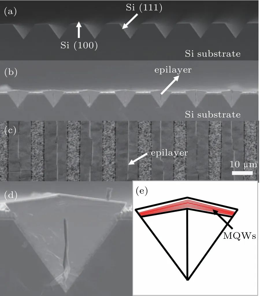
Fig. 2. Cross-sectional SEM images of (a) array of (111)-plane V-grooves in a Si(100)substrate and(b)as-grown epilayer from panel(a). Plan-view SEM images of(c)as-grown epilayer and(d)cross-section of SEM epilayer in V-groove. (e)Schematic cross-section of micro-stripe.
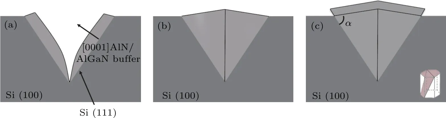
Fig.3. Schematic epitaxial growth showing(a)c-plane AlN/AlGaN buffer growth on Si(111)planes on Si(100)substrate,(b)GaN growth on trench,and(c)semi-polar growth.
To explore the nature of the wideband LED, the crosssectional TEM images are taken on the (1¯101) plane, and shown in Fig.4. Figures 4(a)and 4(b)show the high-magnification cross-sectional TEM images of InGaN/GaN MQWs,and the bright and dark layers indicate the InGaN quantum wells and GaN quantum barriers, respectively. Figure 3(a)corresponds to the center of the stripe, while figure 4(b) corresponds to the side of the stripe. More information about the width related to the embedded MQWs can be obtained from Figs.4(a)and 4(b). In Fig.4(a),the width of the InGaN QWs is 3.45 nm, whereas that of the InGaN QWs in Fig. 4(b) is 1.57 nm. Figure 4(c) shows the positions at which the images in panels (a) and (b) are acquired. The width of the In-GaN/GaN MQWs decreases gradually along the [1¯101]zone axis. Figure 4(c) shows the MQW portion of the epitaxial layer;the dashed lines indicate the boundaries of the MQWs,showing how the width of the surface MQWs changes from the center to the side of the(1¯101)plane. As shown in Fig.4(c),the width of the MQWs decreases from the center to the side.Besides,many black quantum dots appear in InGaN/GaN MQWs. After EDX analysis,it is found that the compositions of these black spots are all indium and the indium phase separation may be used to explain their formation.[43]Figure 4(d)shows the TEM-EDX line scan analysis, and it is interesting that the indium content in the center is much higher than that on the side. The result shows that the indium concentration at the center position is about 10%higher than that on the side.Wider QWs and more indium precipitation in the center of stripe causes the different indium content along the stripe.The MQWs with different indium content may be responsible for the wideband emissions.
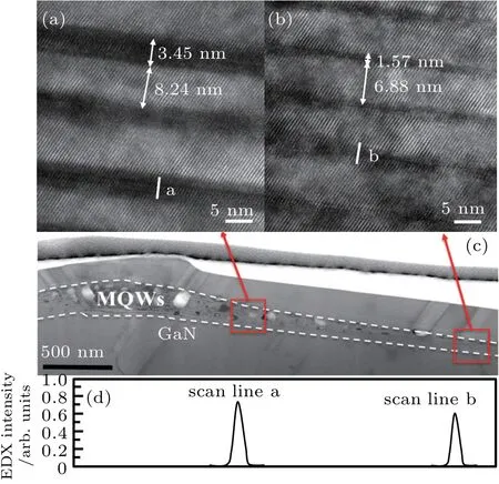
Fig.4. (a)and(b)High-magnification cross-sectional TEM images of MQW portion, which corresponds to different parts (red squares) of panel (c). (c)TEM of MQWs portion revealing individual InGaN/GaN QWs.Dashed lines indicate the boundaries of the MQWs. (d) TEM-EDX lines scanning in direction perpendicular to QW: Line a and line b representing the center and the side of the stripe,respectively.
We also study the optical properties of semi-polar LED structures by cathodoluminescence (CL) spectroscopy. As shown in Fig.5,the origins of individual spectral peaks within an LED structure grown on patterned Si (100) are identified.Figure 5(d) shows 1-µm-resolution CL spot scanning along the white dots denoted respectively as A, B, C, D, and E in Fig.5(a).The emission wavelengths undergo a blue-shift from the center (A) to the side (E) of the (1¯101) plane. The dualcolor emission peaks appear in the center region,whereas only blue emission appears in the remaining side. We apply the CL-image to a single groove with an acceleration voltage of 5 kV at room temperature to obtain the spatial distribution of the indium content as well as the emission wavelengths.These results are shown in Figs.5(b)and 5(c),where the dotted red line represents the merging area in the center, further demonstrate the characteristic of the dependence of QW stripe emission on position:uniform emission occurs over the whole stripe for λ =450 nm.Conversely,the emission comes mainly from the center of the stripe for λ =560 nm. The nonuniform emission is attributed to the nonuniform InGaN MQWs on the semi-polar(1¯101)plane,which contains various indium content. These results are consistent with the above TEM results and demonstrate the nature of the wideband emission LEDs. One should believe that there are several reasons for the wideband emission. Firstly, the angle between the semipolar(1¯101)plane and the Si(100)direction is measured to be 7°,the width of the MQWs portion and indium content in In-GaN/GaN MQWs gradually decrease along the (1¯101) plane(as shown in Fig. 4). Secondly, the short-wavelength emission on the side may be attributed to lattice-pulling effects.[44]When the n-GaN grows,the strain is generated and gathers in the lateral zones. This effect leads to a lower indium incorporation in these areas. What is more, the indium-riched points exist in these wells as shown in Figs.4(c)and 5(c),the strain relaxation of thicker InGaN in the center region is responsible for the indium-riched points,which cause the surface morphology and InGaN/GaN wells to degrade.

Fig. 5. (a) SEM images of single stripe from the center (a) to the side (e).Monochromatic CL mapping images at wavelengths of (b) 450 nm and (c)560 nm. (d)Normalized emission intensity from points A-E in panel(a).
To investigate the electrical properties of the LED structures, we fabricate the lateral-LED devices as shown in the inset (i) of Fig. 6(a). Upon the injection of 350-mA forward current, the white light is obtained by the mixing of the two emission peaks as clearly seen in the inset (ii) of Fig. 6(a).Due to the strong light absorption of silicon substrate, the LED light intensity is relatively weak. Figure 6(a)shows the electroluminescence spectra of semi-polar white LED. Each curve is composed of a strong peak in short wavelength(peak 1, 525 nm-550 nm) and a weak shoulder peak in long wavelength (peak 2, around 575 nm). When the current increases from 50 mA to 80 mA, peak 1 has a rapid blue shift from 570 nm to 530 nm. Such a big blue shift of peak 1 should be due to the band filling of the carrier localization states.[45]In the case of low current, the carriers are injected into the high indium content region (the center of V-groove) and re-combined with each other; as the current increases, the carriers gradually fill the low indium content region (the side of V-groove), thereby leading to a large blue-shift. Then, as the current further increases to 90 mA, peak 1 is basically stable at around 525 nm. As the current increases from 50 mA to 90 mA,peak 2 slowly increases from 575 nm to 580 nm. Figure 6(b)shows the CIE color coordinates taken from the LEDs driven with 350 mA/cm2. The CIE x-and y-chromaticity coordinates are 0.24 and 0.34,respectively. This point is close to white light emission. There are some differences between the EL of our white light LED and the previously reported white light LED.[46]The emissions from our white LEDs are located near the green region,which should be due to a relatively small luminescence area of the high indium content MQW in the center of the V-groove and correspondingly a low proportion in long wavelength emission between 575 nm-600 nm.
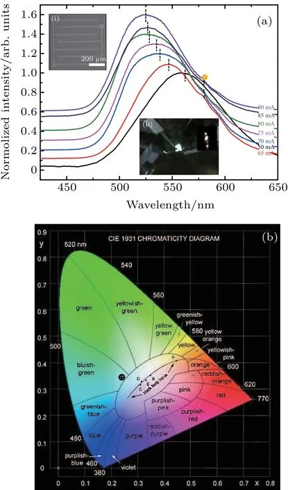
Fig. 6. (a) EL spectra with inset (i) exhibiting reference array of LEDs for various injected current densities,and inset(ii)showing a photograph of LED with injection current of 350 mA/cm2. (b) Typical CIE color coordinates taken from the LEDs driven with 350 mA/cm2.
4. Conclusions
In this work, we obtain wideband emission by growing semi-polar InGaN/GaN MQWs on a patterned micro-striped Si (100) substrate and realize monolithic near white lightemitting diodes. The MQWs are angled with respect to the plane, causing the indium content of the MQWs to gradually vary. The difference in indium content,caused by the variable width of MQWs and indium phase separation,plays a decisive role in determining the characteristics of the monolithic semipolar white InGaN/GaN LED, which uses no luminophores.From a CL analysis, we find the blue emission from the side of the(1¯101)plane and yellow emission from the center of the(1¯101)plane. The wide EL emission and CIE results are well explained by comparing with the CL results. This proposed structure is a promising advance for the fabrication of monolithic semi-polar InGaN/GaN-based near white light-emitting devices without luminophores on Si(100)substrates.
猜你喜欢
应用数学(2022年1期)2022-01-19
参花(下)(2021年1期)2021-12-26
当代工人(2021年11期)2021-10-15
锦绣·上旬刊(2020年3期)2020-06-08
当代旅游(下旬)(2018年5期)2018-10-21
智富时代(2018年1期)2018-03-26
智富时代(2018年1期)2018-03-26
故事作文·高年级(2017年2期)2017-03-01

- Chinese Physics B的其它文章
- Lorentz transmission electron microscopy for magnetic skyrmions imaging∗
- Spin transport in antiferromagnetic insulators∗
- First-principles study of the band gap tuning and doping control in CdSexTe1-x alloy for high efficiency solar cell∗
- Non-Stokes drag coefficient in single-particle electrophoresis:New insights on a classical problem
- SymTopo: An automatic tool for calculating topological properties of nonmagnetic crystalline materials∗
- Tunable coupling between Xmon qubit and coplanar waveguide resonator∗