一种补偿阈值电压和迁移率变化的像素电路设计
2019-12-05 08:35黄勇关肖飞张立文李月华王新林何红宇
智能计算机与应用 2019年5期
黄勇 关肖飞 张立文 李月华 王新林 何红宇


摘 要:本文通过对数据输入阶段的时序进行调整,改进了一种适用于低温多晶硅薄膜晶体管的电压编程型像素电路,用来得到稳定的驱动电流。该像素电路由4个开关薄膜晶体管,1个驱动薄膜晶体管,2个电容和2条控制线组成。理论分析表明,该电路不仅能补偿驱动管阈值电压的变化,而且能补偿驱动管迁移率的变化。仿真结果表明,驱动管的阈值电压变化±0.5 V时,驱动电流变化约为9%,驱动管的迁移率变化±30%时,驱动电流变化约为6%,因此,本电路达到了稳定驱动电流的效果。
关键词: 像素电路;多晶硅薄膜晶体管;阈值电压;迁移率
【Abstract】 A voltage-programming pixel circuit suitable for low-temperature polysilicon thin film transistors is improved to obtain the stable driving current by adjusting the timing in the data input stage. The pixel circuit consists of four switching thin film transistors, one driving thin film transistor, two capacitors, and two control lines. Theoretical analysis shows that the circuit not only can compensate the threshold voltage variation of the driving transistor, but also can compensate the mobility variation of the driving transistor. The simulation results show that, the driving current variation is about 9% when the threshold voltage variation of the driving transistor is ±0.5 V, and the variation of the driving current is about 6% when the mobility variation of the driving transistor is ±30%. Thus, the present circuit can achieve the stable driving current.
【Key words】 pixel circuit; polysilicon thin film transistor; threshold voltage; mobility
0 引 言
在高分辨率、中小尺寸显示技术中,低温多晶硅薄膜晶体管得到了广泛的应用。这种晶体管具有迁移率高、驱动能力强等优点[1]。但是,在像素电路矩阵中,由于受制造工艺的局限和长时间工作时应力的影响,晶体管的电学特性会表现出不均匀性[2]。这种不均匀性一般表现为驱动管阈值电压和迁移率的变化,因此,需要设计合适的像素电路进行补偿。
补偿驱动管阈值电压和迁移率变化的像素电路分为电流编程型和电压编程型[3]。
Lee等人[4]提出了一种电流编程型像素电路,该电路时序简单,但电流编程型像素电路充放电时间较长,可能会导致数据写入不充分,影响正常显示。
电压编程型像素电路具有充放电时间短的特点,因此,得到了业界的高度重视。文献[5-7]提出了补偿阈值电压和迁移率变化的像素电路,这些电路具有结构简单的优点,但需要增加迁移率补偿阶段,导致时序比较复杂。因而,人们提出了多种不必增加迁移率补偿阶段的方法:文献[8-12]把迁移率的变化转化为栅极电位或源级电位的变化;Yamamoto等人[13]调整阈值电压提取阶段的时序;Liao等人[14]构造驱动管的镜像;Yi等人[15]引入OLED阳极电压;Lin等人[16]调整数据输入阶段的时序。上述方法在补偿阈值电压和迁移率的变化方面都有自己的特色。
研究注意到,Yao等人[17]提出了一种补偿阈值电压变化的像素电路,但没有涉及迁移率变化的问题,有待进一步完善。
本文对数据输入阶段的时序进行调整,在Yao电路的基础上[17],实现了对阈值电压和迁移率变化的补偿。理论分析和仿真验证结果表明,本电路能够稳定驱动电流,达到了补偿效果。
1 像素电路结构和工作原理
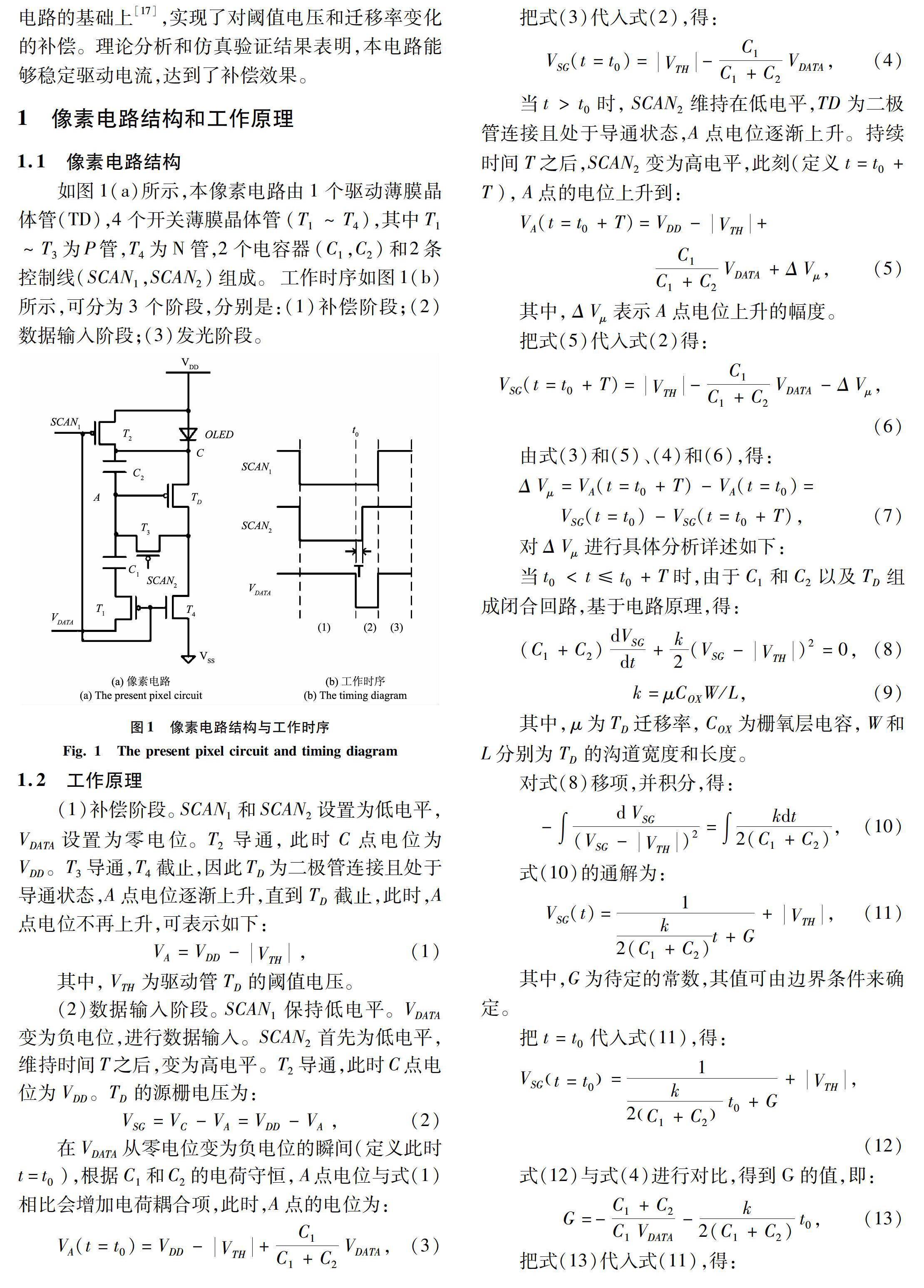
1.1 像素电路结构
如图1(a)所示,本像素电路由1个驱动薄膜晶体管(TD),4个开关薄膜晶体管(T1~T4),其中T1~T3为P管,T4为N管,2个电容器(C1,C2)和2条控制线(SCAN1,SCAN2)组成。工作时序如图1(b)所示,可分为3个阶段,分别是:(1)补偿阶段;(2)数据输入阶段;(3)发光阶段。
3 結束语
本文在数据输入阶段,通过对电路时序进行调整,改进了一种电压编程型像素电路,理论分析了补偿阈值电压和迁移率变化的原理,仿真验证结果表明,本电路能有效补偿阈值电压和迁移率的变化,达到了稳定驱动电流的效果。
参考文献
[1]NAM W J, LEE J H, KIM C Y, et al. High-aperture pixel design employing VDD line elimination for active matrix organic light emitting diode display [J]. Japanese Journal of Applied Physics, 2006, 45(4): 2433-2436.
[2]JUNG S H, NAM W J, HAN M K. A new voltage-modulated AMOED pixel design compensating for threshold voltage variation in Poly-Si TFTs [J]. IEEE Electron Device Letters, 2004, 33(10): 690-692.
[3]DAWSON R M A , SHEN Z , FURST D A , et al. The impact of the transient response of organic light emitting diodes on the design of active matrix OLED displays [C] // International Electron Devices Meeting. San Francisco, USA: IEDM, 1998: 32.6.1-32.6.4.
[4]LEE J H , NAM W J, JUNG S H , et al. A new current scaling pixel circuit for AMOLED [J]. IEEE Electron Device Letters, 2004, 25(5): 280-282.
[5]PARK Y J, JUNG M H, PARK S H, et al. Voltage-programming-based pixel circuit to compensate for threshold voltage and mobility using natural capacitance of organic light-emitting diode [J]. Japanese Journal of Applied Physics, 2010, 49(3): 03CD01-1-03CD01-5.
[6]ONOYAMA Y, YAMASHITA J, KITAGAWA H, et al. 0.5-inch XGA Micro-OLED display on a silicon backplane with high-definition technologies [J]. Sid Symposium Digest of Technical Papers, 2012, 43(1): 950-953.
[7]KANG C K, CHOI B D. A pixel circuit for AMOLED displays compensating for threshold voltage and mobility variation [C] // International Display Workshops 2013. Sapporo, Japan: IDW, 2013 :433-436.
[8]SONG S J, NAM H. In pixel mobility compensation scheme for AMOLED pixel circuits [J]. Journal of Display Technology, 2015, 11(2): 209-213.
[9]KIM Y, KANICKI J, LEE H. An a-InGaZnO TFT pixel circuit compensating threshold voltage and mobility variations in AMOLEDs [J]. Journal of Display Technology, 2014, 10(5): 402-406.
[10]LIAO Zhiqiang, LIN Hesheng, LIU Binjie, et al. Mobility variation and threshold voltage shift immunized amorphous-indium-gallium-zinc-oxide pixel circuit [C] // IEEE International Conference on Electron Devices and Solid-State Circuits. HongKong, China: EDSSC, 2016: 255-258.
[11]YI Shuiping, WU Jixiang, LIAO Congwei, et al. An a-IGZO TFT AMOLED pixel circuit to compensate threshold voltage and mobility variations [C] // International Workshop on Active-Matrix Flat Panel Displays and Devices 2018. Kyoto, Japan: IEEE, 2018: 1-4.
[12]LIN C L, HUNG C C, CHEN P S, et al. New voltage-programmed AMOLED pixel circuit to compensate for nonuniform electrical characteristics of LTPS TFTs and voltage drop in power line [J]. IEEE Transactions on Electron Devices, 2014, 61(7): 2454-2458.
[13]YAMAMOTO T,YAMASHITA J,YUMOTO A,et al. Novel pixel circuit and driving method of AM-OLED for mobile application pixel circuit for threshold voltage and mobility compensation with compensation with IGZO TFTs [C] // Proc. SPIE 6333, Organic Light Emitting Materials and Devices X, 633309. California, United States: OLEMD, 2006: 633309-1-633309-8.
[14]LIAO C, DENG W, SONG D, et al. Mirrored OLED pixel circuit for threshold voltage and mobility compensation with IGZO TFTs [J]. Microelectronics Journal, 2015, 46(10): 923-927.
[15]YI Shuiping, HUO Xinxin, LIAO Congwei, et al. An a-IGZO TFT pixel circuit for AMOLED display systems with compensation for mobility and threshold voltage variations [C] // 2018 IEEE International Conference on Electron Devices and Solid State Circuits. Shenzhen, China: EDSSC,2018: 1-2.
[16]LIN C L, LAI P C, DENG M Y. New pixel circuit to improve current uniformity for high-resolution AMOLED displays [J]. SID Symposium Digest of Technical Papers, 2015, 46(1): 1297-1300.
[17]YAO Rihui, ZHANG Lirong, ZHOU Lei, et al. A new compensation pixel circuit with all-p-type TFTs for AMOLED displays [J]. Displays, 2013, 34(3): 187-191.