
Effect of radio-frequency power on the characteristics of MgO doped gallium-zinc oxide thin films
2019-12-26 02:04GUJinhuaLUZhouZHUYaCHENShoubu
中南民族大学学报(自然科学版) 2019年4期
GU Jinhua, LU Zhou, ZHU Ya, CHEN Shoubu
(1 Experimental Teaching and Laboratory Management Center, South-Central University for Nationalities, Wuhan 430074, China;2 College of Electronic Information Engineering, South-Central University for Nationalities, Wuhan 430074, China)
Abstract The thin films of MgO doped gallium-zinc oxide were prepared using magnetron sputtering technique. The effect of radio-frequency power on the microstructure and electrical characteristics of the deposited thin films was investigated by X-ray diffraction (XRD), electrical resistivity, carrier concentration and Hall mobility measurements. The experimental results demonstrate that all the deposited thin films have hexagonal wurtzite structure with highly c-axis orientation. The radio-frequency power significantly affects the microstructure and electrical characteristics of the deposited thin films. When the radio-frequency power is 125 W, the thin film possesses the best crystalline quality and electrical characteristics, with the largest crystallite size of 52.1 nm, the minimum tensile stress of 0.082 GPa, the lowest electrical resistivity of 1.5410-3 Ω·cm, the maximum carrier concentration of 5.261020 cm-3 and the highest Hall mobility of 7.41 cm2V-1s-1.
Keywords gallium-zinc oxide; doping; electrical properties
Gallium-zinc oxide is a promising transparent conductive film material for applications as transparentelectrodes in light-emitting diodes[1-3], solar cells[4-6], touch screens[7], microsensors[8,9], plasma display panels[10,11]and acousto-optic devices[12,13]. Besides high conductivity and optical transmittance in the visible region, the gallium-zinc oxide thin films have a lot of advantages such as high abundance, non-toxicity, low cost and high stability under the hydrogen plasma compared to indium-tin oxide thin films[14]. For the preparation of gallium-zinc oxide thin films, there are many deposition techniques currently in use, for example, direct-current magnetron sputtering[15], radio-frequency magnetron sputtering[16-18], hydrothermal process[19], atomic layer deposition[20,21], molecular beam epitaxy[22], pulsed laser ablation[23]and reactive plasma deposition[24]. Among all these methods, radio-frequency magnetron sputtering is promising in preparing transparent conductive gallium-zinc oxide thin films, due to the low cost of the source materials, the high deposition rates, the good surface flatness and the simplicity of the growth process required.
In the present work, the thin film samples of MgO doped gallium-zinc oxide were prepared on glass substrates by radio-frequency magnetron sputtering technique at different powers. The microstructure and electrical characteristics of the thin films were studied in detail.
1 Experimental procedure
Commercial plane glasses were cut into 3×3 cm2plates and used as substrates in this experiment. Prior to their use, the glass substrates were successively washed in an ultrasonic bath of acetone, alcohol and deionized water, each for 15 min, and then dried in a high-purity nitrogen gas jet. The thin film samples of MgO doped gallium-zinc oxide were prepared on the previously cleaned glass substrates by radio-frequency magnetron sputtering system (MS-560C) using a sintered ceramic target with a diameter of 5 cm. The following compositions were chosen: 2 wt.% MgO + 96 wt.% ZnO + 2 wt.% Ga2O3. Raw materials were MgO, ZnO and Ga2O3powders (99.99% in purity). Before deposition, the chamber was evacuated to an ultimate background pressure of 4.5×10⁻⁴Pa using a turbo molecular pump. Then high-purity (99.999%) argon gas was introduced into the chamber at a fixed flow rate of 25 sccm, and argon pressure was maintained at 3.5 Pa. Then 10 min pre-sputtering with the glass substrate covered by a closely mounted shutter was employed to clean contamination on the target surface, followed by true sputtering. During deposition, the substrate temperature was fixed at 550 K, and the distance between the target and the substrate was kept at 7.5 cm. In order to investigate the influcnce of radio-frequency power on the characteristics of the deposited thin films, the radio-frequency power was changed from 100 W to 175 W.
The X-ray diffraction (XRD) patterns of the thin films were recorded with a Bruker advanced D8 diffractometer using standard Cu Kαradiation (λ=0.15406 nm). The scan range was 20-70with 0.0164steps. The crystallite phase was evaluated with the data of Joint Committee on Powder Diffraction Standards (JCPDS). The carrier concentration, Hall mobility and electrical resistivity of the thin films were measured by a Hall effect measurement system (RH-2035) using the Van der Pauw technique at room temperature.
2 Results and discussion
Fig.1 gives the XRD patterns of the thin films prepared at different radio-frequency powers.The XRD peaks are assigned to ZnO according to the Joint Committee of Powder Diffraction Standards Card (JCPDS 36-1451)[25]. From the figure, only the (002) diffraction peak was exhibited for all the deposited samples, and the peak location is at about 34.5(2θ) (peak location of the standard powder ZnO specimen is 34.42). No additional peaks were found as the radio-frequency power increases up to 175 W. It is also seen that the peak intensity increases with increasing radio-frequency power up to 125 W, and then the intensity of the (002) peak decreases for a higher radio-frequency power of 150 W and 175 W. The thin film deposited at 125 W has the maximum intensity of (002) peak. Note also that neither metallic Mg or Ga characteristic peaks nor MgO or Ga2O3peaks was observed from the XRD patterns, which implies that the dopants have not destroyed the ZnO structure and act as typical dopants. The results imply that all the thin films have a polycrystalline hexagonal wurtzite structure, and thec-axis is a strong preferred orientation.

Fig.1 XRD patterns of the deposited samples prepared at radio-frequencypower of (a) 100 W,(b) 125 W, (c) 150 W and (d) 175 W, respectively图1 功率(a) 100 W, (b) 125 W, (c) 150 W和(d)175 W时样品的XRD图谱
To assess the quality of the deposited thin films, the values of the full-width at half-maximum (FWHM) of (002) peak and the crystallite size (D) were used. TheDvalues were determined according to the Scherrer’s formula[26,27]:
(1)
whereλis the wavelength of X-rays used,θis the Bragg’s diffraction angle at (002) peak position andBis the FWHM in degrees,kis a constant that depends on crystallites shape (kis taken equal to 0.90 in this work). The values ofBandDas a function of radio-frequency power are shown in Fig.2 and Fig.3, respectively. With increasing radio-frequency power from 100 W to 125 W, theBdecreases and theDincreases, suggesting that the crystalline quality of the deposited samples becomes better. However, with further increasing from 125 W to 175 W, theBincreases and theDdecreases, indicating that the crystalline quality deteriorates. It is clear that the sample prepared at the radio-frequency power of 125 W shows the best crystal quality. From the Fig.3, the crystallite size along thec-axis is observed to range from 33.8 nm to 52.1 nm. The sample prepared at 125 W has the minimumBof 0.153and the maximumDof 52.1 nm. The results indicate that the crystalline quality of the deposited thin films is strongly dependent on the radio-frequency power.
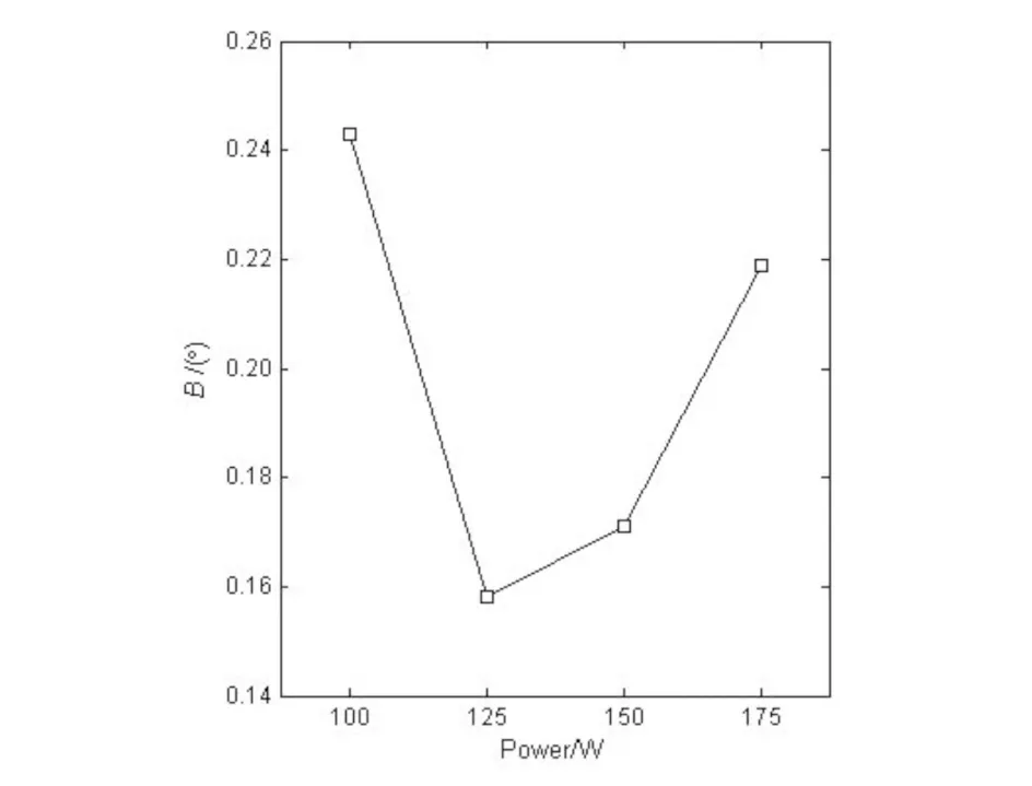
Fig.2 Influence of radio-frequency power on FWHM ofthe deposited samples图2 功率对样品半高宽的影响
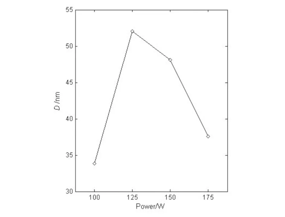
Fig.3 Influence of radio-frequency power on crystallite size of the deposited samples图3 功率对样品晶粒尺寸的影响
The strain (ε) and the stress (σ) of the deposited thin films can be calculated from the following formulae[28,29]:
(2)
σ=-232.8ε(GPa),
(3)
wheredandd0are values of interplanar spacing of the deposited films and pure ZnO, respectively. According to the Eq. (3), if the stressσis positive,the biaxial stress is tensile and if the stress is negative, the biaxial stress is compressive. Thedvalue can be obtained from XRD data by the Bragg’s law[28]:
(4)
whereλis the wavelength of X-rays andθis the diffraction angle.The values ofεandσas a function of radio-frequency power are presented in Fig. 4 and Fig. 5,respectively.As shown in Fig. 5,the nature of stress in plane of the thin film is positive for all samples indicating that the deposited films are in a state of tensile stress. Theεandδvalues of the deposited thin films are found to be in the range of 3.5510-4~9.5310-4and 0.082~0.22 GPa, respectively. Clearly, the sample prepared at the radio-frequency power of 125 W exhibits the minimum value ofεandδ. The decrease inεandδcan be attributed to the improvement of crystallinity and the increase of crystallite size.

Fig.4 Influence of radio-frequency power onstrain ofthe deposited samples图4 功率对样品应变的影响

Fig.5 Influence of radio-frequency power on stress ofthe deposited samples图5 功率对样品应力的影响
The variation of electrical resistivity (ρ), carrier concentration (ne) and Hall mobility (μ) as a function of radio-frequency power are given in Figs. 6-8, respectively. From Fig.6, we note that theρvalue decreases with the radio-frequency power increasing from 100 W to 125 W, reaches to the minimum value of 1.5410-3Ω·cm at 125 W, and thereafter increases to 6.3710-3Ω·cm at 175 W. An opposite trend is observed in bothneandμof the deposited samples as shown in Figs. 7-8. When the radio-frequency power is 125 W, the deposited sample exhibits the best electrical properties, with the lowest electrical resistivity of 1.5410-3Ω·cm, the maximum carrier concentration of 5.261020cm-3and the highest Hall mobility of 7.41 cm2V-1s-1. The results suggest that the electrical characteristics of the deposited thin films depend on the radio-frequency power significantly.
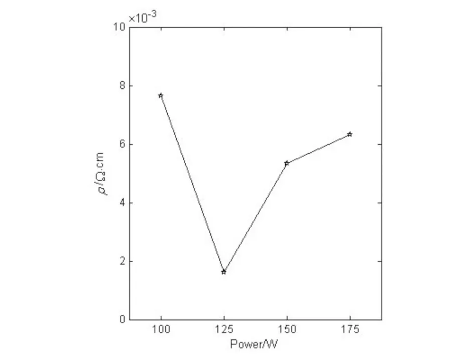
Fig.6 Influence of radio-frequency power onelectrical resistivity of the deposited samples图6 功率对样品电阻率的影响
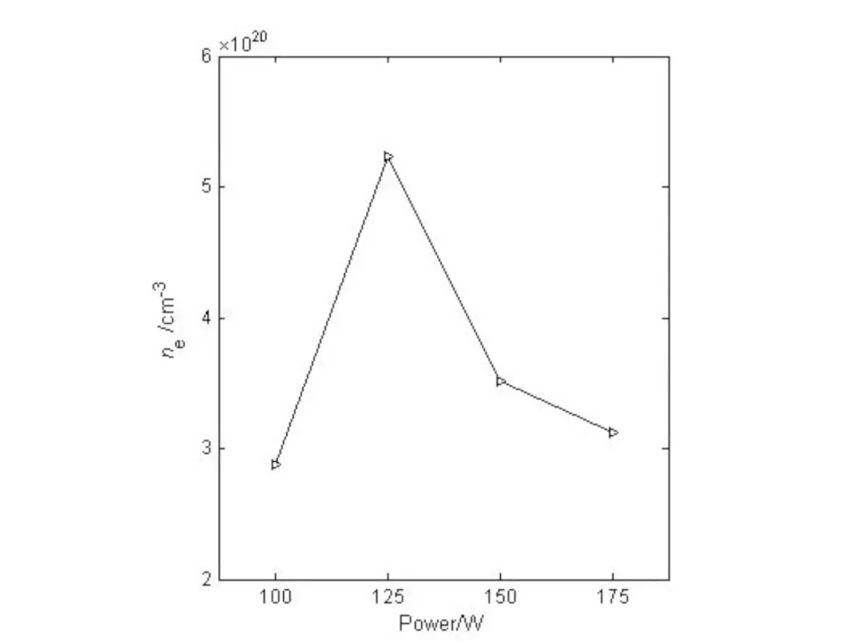
Fig.7 Influence of radio-frequency power oncarrier concentration of the deposited samples图7 功率对样品载流子浓度的影响

Fig.8 Influence of radio-frequency power on Hallmobility of the deposited samples图8 功率对样品载流子迁移率的影响
3 Conclusion
In this study, the thin films of MgO doped gallium-zinc oxide were prepared by magnetron sputtering method, and the effect of the radio-frequency power on the microstructure and electrical characteristics was investigated. It is observed that all thedeposited thin films have hexagonal wurtzite structure with highlyc-axis orientation. The thin film prepared at the radio-frequency power of 125 W possesses the best crystallinity and electrical characteristics, which have the largest crystallite size (52.1 nm), the minimum tensile stress (0.082 GPa), the lowest electrical resistivity (1.5410-3Ω·cm), the maximum carrier concentration (5.261020cm-3) and the highest Hall mobility (7.41 cm2V-1s-1). The experimental results demonstrate that the crystallite quality and electrical characteristics of the deposited thin films are highly dependent upon the radio-frequency power.
猜你喜欢
物探与化探(2022年2期)2022-04-28
物理学报(2022年6期)2022-03-30
防爆电机(2021年3期)2021-07-21
煤气与热力(2021年3期)2021-06-09
科学技术创新(2021年14期)2021-05-28
物理学报(2020年16期)2020-08-29
物理学报(2019年16期)2019-08-29
湖北农业科学(2019年11期)2019-07-22
商情(2019年26期)2019-06-25
科技风(2018年9期)2018-05-14
