
CdS/Si nanofilm heterojunctions based on amorphous silicon films:Fabrication,structures,and electrical properties∗
2021-03-11 08:33YongLi李勇PengFeiJi姬鹏飞YueLiSong宋月丽FengQunZhou周丰群HongChunHuang黄宏春andShuQingYuan袁书卿
Chinese Physics B 2021年2期
关键词:李勇
Yong Li(李勇), Peng-Fei Ji(姬鹏飞), Yue-Li Song(宋月丽),Feng-Qun Zhou(周丰群), Hong-Chun Huang(黄宏春), and Shu-Qing Yuan(袁书卿)
Laboratory of Nano Optoelectronic Materials and Insulation Materials,Pingdingshan University,Pingdingshan 467000,China
Keywords: magnetron sputtering,CdS/Si nanofilm heterojunctions,electron behaviors,SCLC mechanisms
1. Introduction
The heterojunction is an important structure which can control the carrier transportation to perform the different functions and be applied to the fields of solar cells and light emitting diodes.[1,2]Under the sun, the heterojunction can absorb the photons to produce the photo-generated carrier pairs. And with the help of built-in potential,the photo-generated carrier pairs can be separated, transported and collected to turn into electricity.[3–5]Under the applied voltage,the injected carriers in the heterojunction can be recombined between the valence band and conduction band, between the different defect levels, as well as between the different semiconductors, to emit the photons with the different energy values to realize the light emissions with the different wavelengths.[6,7]
The CdS is a vital and classical II–VI semiconductor compound featuring the direct band gap, relative low work function, excellent transport properties, and high electronic mobility.[8]It is indicated that the CdS is a prominent electronic and optoelectronic material.[9,10]Silicon is also an important optoelectronic semiconductor material.[11–13]Since CdS/Si heterojunction was constructed in 1967,[14]it has received much attention from the researchers.[7,15–18]The photovoltaic properties of CdS/Si heterojunction have been studied in depth. The energy conversion efficiency has been improved from 4.9%by Okimura[14]to 12.29%by Cai.[19]In addition,the photodetector and light emitting diodes based on CdS/Si heterojucntion have been widely investigated.[7,16,20,21]However, the energy conversion efficiency of solar cells based on CdS/Si heterojunction is still low. So, the interface engineering, energy band engineering and doping technology are studied to modulate and improve the performance of CdS/Si heterojunction.[19,22,23]As is well known, the carriers in the transportation can be trapped outside the depletion region to deteriorate the performance of devices due to the thicker layers of p-/n-type materials.[2]Therefore,it will also be a way to improve the performance of CdS/Si heterojunction through reducing the thickness of p-/n-type materials and shortening the transportation distance from the depletion region to the electrode,and thus reducing the trapped probability of carriers.
In the present work, the CdS/Si nanofilm heterojunctions is fabricated by using the radio frequency (RF) magnetron sputtering technology. Their structures are studied by emission scanning electron microscopy (SEM) images, highresolution transmission electron microscope (HR-TEM) images, x-ray diffraction (XRD) spectra and x-ray photoelectron spectroscopy(XPS)spectra. Through analyzing the current density–voltage(I–V)characteristics,the transport mechanisms are discussed in detail.
2. Experiments
The amorphous silicon nanofilms and CdS nanofilms have been deposited on an ITO glass in turn by using an RF magnetron sputtering method. Silicon target with the boron doping and a resistivity between 1.0 Ω·cm and 10.0 Ω·cm and CdS target(99.99%), have been produced in the Chinese Zhongjinyan Company.The distance is 5.0 cm from the targets to the ITO glass. Detailed fabrication process is described as follows. Firstly,the silicon target and CdS target were placed at A and B sputtering positions, respectively. And the sputtering chamber was pumped to less than 10−5Pa. The argon gas was fed into the chamber and the gas pressure was maintained at 1.0 Pa. The sputtering power applied to the silicon target was 45 W.The sputtering processes of silicon films lasted 20 min. After the silicon films was fabricated, the silicon target was replaced by CdS target. Then the sputtering power of 60 W was applied to the CdS target. The sputtering time of CdS film was 20 min. Two Ag electrodes were fabricated by a direct current magnetron sputtering method.
The structural properties of the amorphous silicon films were characterized by the XRD(PanalyticalX’Pert Pro)where Cu-Kα was used as an x-ray source (λ = 1.5046 ˚A), the field emission scanning electron microscopy (FESEM, JSM 6700F), and HR-TEM (JEM-2100). The elemental compositions and chemical valence states of the amorphous silicon films and the CdS–Si interface are analyzed by XPS(Axis Ultra, Kratos). The electrical properties with current density vs voltage were measured by a Keithley SOURCEMETER-2400 system.All data about I–V curves were recorded at room temperature.
3. Results and discussion
The XRD patterns of the amorphous silicon and the CdS/Si nanofilm heterojunctions are displayed in Fig.1. Form Fig.1(a),a wide band can be observed to be located between~15◦and ~35◦, indicating that the fabricated silicon has an amorphous silicon structure or amorphous SiOxstructure.A set of diffraction peaks can be observed from Fig.1(b)to be located at 24.8◦, 26.6◦, 28.1◦, 36.6◦, 43.6◦, 47.9◦,and 51.8◦, respectively, corresponding to (100), (002), (101),(102), (110), (103), and (112) diffraction peaks of hexagonal CdS(JCPDS:01-077-2306). In the present work,the intensity of (002) diffraction peak is much greater than other diffraction peaks’, indicating that the CdS films grow preferentially along the c axis.[24]By analyzing the XRD data,the interplanar spacing dhkland lattice constants (a and c) of hexagonal CdS can be obtained from the following equations:[25]
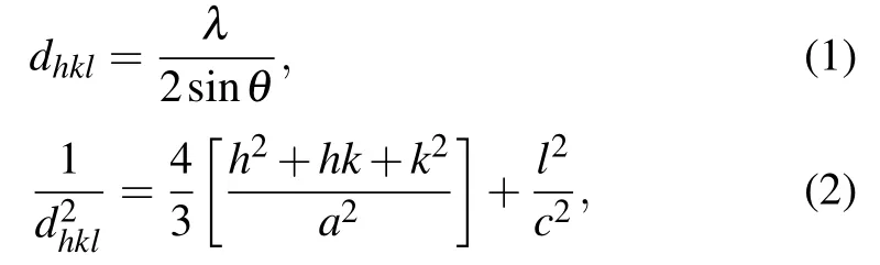
where(hkl)are the Miller indices and λ is the wavelength of the x-ray. From Eqs.(1)and(2),we can obtain the hexagonal lattices with a=3.98 ˚A and c=6.83 ˚A.Comparing with the bulk CdS(a=4.14 ˚A and c=6.715 ˚A),the variation of the lattice constants suggests that the microstrain and surface defects should be existent due to the effect of amorphous silicon/SiOxat the interface of heterojunctions.
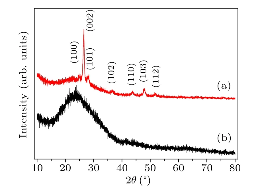
Fig.1. XRD patterns from(a)amorphous silicon and(b)CdS/Si nanofilm heterojunctions.
In this work,the fabricated silicon films are always placed in the argon atmosphere of 1.0 Pa until the CdS films are fabricated. No oxygenis added into the fabrication process. In the XRD pattern of heterojunctions (Fig.1(b)), however, the diffraction peaks of silicon cannot be found even in the thinner CdS films. So,the sputtered silicon films have amorphous structures.
To investigate the morphological and structural properties of amorphous silicon and CdS/Si nanofilm heterojunctions,the samples are investigated by SEM and HR-TEM as shown in Fig.2. From Fig.2(a), nano rods can be observed, which are characterized with the lengths in a range of 65 nm–100 nm and diameters in a range of 15 nm–30 nm and randomly distributed. The morphology of CdS/Si nanofilm heterojunctions is shown in Fig.2(b). The particle-shaped structure can be observed, whose average size is ~88 nm obtained by the statistical method from 45 measuring points. The inset of Fig.2(b)shows the side-view SEM image of CdS/Si nanofilm heterojunctions, from which the thickness values of amorphous silicon layer and CdS film are estimated at ~64 nm and~105 nm, respectively. In order to illuminate the fine structure of heterojunctions, the sample is carefully cleaved and moved on the copper net to measure by TEM.From Fig.2(c),a pillar structure can be observed.The area marked by the arrow is measured by HR-TEM and shown in Fig.2(d).The clear lattice fringes can be observed and the distance is measured to be~0.68 nm and be indexed to the lattice spacing of the planes of 2H-CdS.[26,27]The inset of Fig.2(d) shows the selected-area electron diffraction (SAED) from the marked area. Through analyzing the SAED pattern, it is indicated that the sputtered CdS nanofilms show(002)-orientation growth.[26]
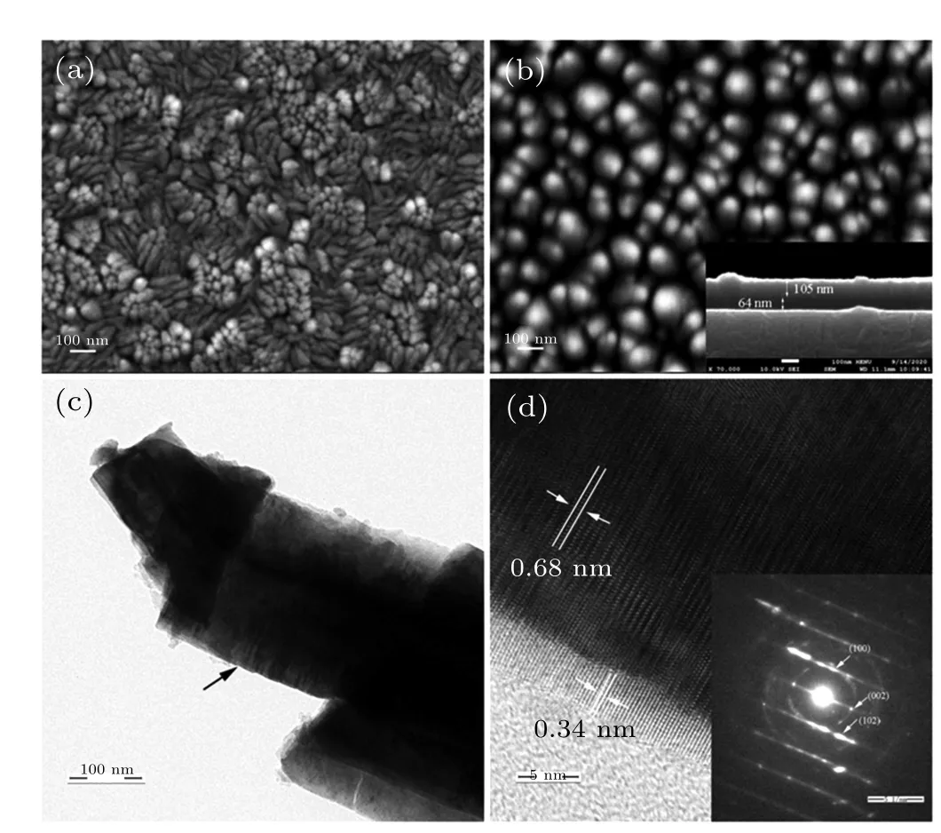
Fig.2. SEM images of(a)amorphous silicon and(b)CdS/Si nanofilm heterojunctions,with inset showing Side-view SEM image. (c)TEM image and(d)HR-TEM image of CdS/Si nanofilm heterojunctions,with inset showing SAED image.
In order to further study the structures,XPS spectra of the amorphous silicon and CdS/Si heterojunctions are measured and shown in Fig.3. From the survey spectra of the amorphous silicon and the interface of CdS/Si nanofilms heterojunctions in Fig.3(a),Si(2p),Si(2s),C(1s),and O(1s)peaks from the amorphous silicon, and Cd (4d), Cd (3d), Cd (3p),S(2p), C(1s), and O(1s)peaks from the CdS/Si heterojunctions can be observed. The fine XPS spectrum of Si(2p)from the amorphous silicon is shown in Fig.3(b), where two wide peaks can be observed. Utilizing the Gauss function fitting method,the XPS spectrum of Si(2p)can be decomposed into three peaks which are located at ~98.72 eV, ~101.43 eV,and ~102.61 eV,respectively,and are indexed to the valence states of Si0, Si2+, and Si4+.[28]Figure 3(c) shows the fine XPS spectrum of Si(2p)from the interface of CdS/Si nanofilm heterojunction. Only a peak located at ~98.19 eV can be observed,which is confirmed to originate from the valence state of Si0. For Fig.3(b), however, there are three different valence states for silicon. The Si2+and Si4+are existent due to the introduction of oxygen into the process (from sputtering chamber to the XPS test system). Because only the valence state of Si0can be observed at the interface of CdS/Si nanofilm heterojunctions. Figure 3(d) shows the fine spectra of S(2p)and Cd(3d).[29,30]The peaks located at ~404.91 eV and ~411.67 eV are corresponding to the binding energy of Cd(3d5/2)and Cd(3d3/2),respectively.[19]
Fig.3. XPS spectra from amorphous silicon and CdS/Si nanofilm heterojunctions,showing(a)XPS spectra,(b)fine XPS spectra of Si from amorphous silicon,(c)fine XPS spectra of Si from CdS/Si nanofilm heterojunciton interface,and(d)fine XPS spectra of S and Cd.
The analysis of the current density–voltage characteristics is extremely useful in identifying the electron transport mechanisms and determining the fundamental properties of heterojunctions,such as free carrier density and defect state distribution.[31–33]So, the dark I–V curve from CdS/Si nanofilm heterojunctions is measured and recorded at room temperature as shown in Fig.4(a). The schematic diagram of CdS/Si nanofilm heterojunctions is shown in the inset of Fig.4(a). Form the I–V curve,the parameters,such as the onset voltage of ~3.36 V at current density of ~0.001 A·cm−2,the forward current density of ~0.1737 A·cm−2at forward voltage of 5.0 V, and the leakage current density of~0.0006 A·cm−2at a reverse voltage of 5.0 V, can be extracted and analyzed. The forward-to-reverse current ratio is calculated to be ~290 at±5.0 V.The onset voltage of CdS/Si nanofilm heterojunctions in the present work is higher than those of the previous reports.[22,24]Through analyzing all experimental data, the higher resistance of amorphous silicon hinders the electron transportation in the heterojunctions,and leads to the higher onset voltage. And also there appear lots of defects in the amorphous silicon films.[12]How to optimize the fabrication of amorphous silicon films to reduce the defect states is one of the subjects of our future study.
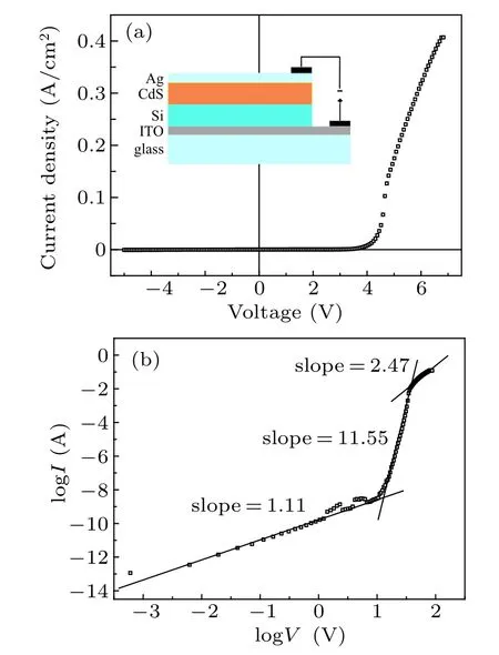
Fig.4. (a) Dark I–V curve from CdS/Si nanofilm heterojunctions at room temperature,with inset showing schematic diagram of CdS/Si nanofilm heterojunctions,and(b)double logarithm plotted dark I–V curve.
In order to investigate the electron transportation properties, the double-logarithm plotted I–V curve is shown in Fig.4(b). Three linear regions can be observed,whose slopes are ~1.11,~11.55,and ~2.47 from low forward voltage to high forward voltage, respectively, and are named region A,region B, and region C. Through analyzing the double logarithm plot,the region A and region B are separated by a voltage of ~2.73 V,and the region B and region C are separated by a voltage of ~4.90 V.According to the heterojunction theory,the variation of a current density with voltage can be described by the following equation:[34,35]

When the parameter m is less than 2,the electronic behaviors obey the Ohmic mechanism in which the carriers are mainly contributed by the thermally generated electrons. And when the parameter m is equal to or greater than 2, the electronic behaviors follows the space charge limited current (SCLC)mechanism in which the carriers are mainly contributed by the external electron injection.[32,36]So, the electronic behaviors in region A should conform to the Ohmic mechanism.And the electronic behaviors in region B and region C should comply with the SCLC mechanism.[37,38]Besides,the slope of region B is found to be bigger than that of region C, indicating that when the forward voltage is larger than ~2.73 V,part of traps between the Fermi level and conduction band are occupied,and with the increase of forward voltage (>~4.90 V), most of traps are occupied.
4. Conclusions
In this work, through depositing the amorphous silicon nanofilms and CdS nanofilms in turn by the RF magnetron sputtering method, we prepare the CdS/Si nanofilm heterojunctions. The rectifying effect from CdS/Si nanofilm heterojunctions can be observed obviously. Below the forward voltage of ~2.73 V, the electron behaviors obey Ohmic mechanism. Above the forward voltage of ~2.73 V, the electron behaviors follow the SCLC mechanism.
猜你喜欢
Chinese Physics B(2022年8期)2022-08-31
Chinese Physics B(2022年7期)2022-08-01
小天使·一年级语数英综合(2021年11期)2021-11-23
中国粮食经济(2020年11期)2020-12-23
齐鲁艺苑(2019年5期)2019-11-09
艺术家(2019年2期)2019-03-21
诗潮(2016年2期)2016-03-12

- Chinese Physics B的其它文章
- Novel traveling wave solutions and stability analysis of perturbed Kaup–Newell Schr¨odinger dynamical model and its applications∗
- A local refinement purely meshless scheme for time fractional nonlinear Schr¨odinger equation in irregular geometry region∗
- Coherent-driving-assisted quantum speedup in Markovian channels∗
- Quantifying entanglement in terms of an operational way∗
- Tunable ponderomotive squeezing in an optomechanical system with two coupled resonators∗
- State transfer on two-fold Cayley trees via quantum walks∗