
Modeling,simulations,and optimizations of gallium oxide on gallium–nitride Schottky barrier diodes
2021-03-11 08:33TaoFang房涛LingQiLi李灵琪GuangRuiXia夏光睿andHongYuYu于洪宇
Chinese Physics B 2021年2期
Tao Fang(房涛), Ling-Qi Li(李灵琪), Guang-Rui Xia(夏光睿),2,†, and Hong-Yu Yu(于洪宇),‡
1School of Microelectronics,Southern University of Science and Technology,Shenzhen 518055,China
2Department of Materials Engineering,the University of British Columbia,Vancouver,British Columbia,V6T1Z4,Canada
Keywords: technology computer-aided design(TCAD),gallium oxide(Ga2O3),gallium nitride(GaN),Schottky barrier diode(SBD)
1. Introduction
β-gallium oxide(β-Ga2O3)is a wide-bandgap semiconductor with potential applications in high-frequency and highpower devices.[1–3]Among the five polymorphs of Ga2O3,the β-Ga2O3is the most stable.[4]It has a monoclinic structure and belongs to the space groupC2/m.[5]For simplicity,Ga2O3denotes β-Ga2O3in the following text. With the development of Ga2O3epitaxy techniques,two-inchsized Ga2O3substrates have been commercialized,[6]and the n-type doping technique using Sn or Si has been matured.[1]The Ga2O3device fabrication and p-type doping technique are the two major problems in current Ga2O3research.
It is quite hard to isolate the different phases in pure Ga2O3crystalline form.[7]As a result, simulations and calculations have been used to forecast Ga2O3crystal and device properties. For example, He et al. calculated the band structure by density functional theory (DFT).[5]Osipov et al. calculated the structural and elastoplastic properties, including Young’s modulus and linear compressibility.[8]However,the Ga2O3device simulations based on the finite element method have been scarce until now, which is mainly because the Ga2O3is not a well-defined semiconductor material in major device simulation software and wide-bandgap semiconductor simulations are difficult to converge.[9]
In this work,we first conduct a thorough survey of available literature material parameters of Ga2O3and make careful selections and estimations of these parameters.[9,10]We then update the material library of APSYSTMdeveloped by Crosslight Software for our simulations. Also,we select suitable recombination models for gallium oxide and gallium nitride separately. Based on these new definitions, parameter calibrations are performed to fit the available experimental data of gallium–oxide–metal–semiconductor field-effect transistor (MESFET)[11]and gallium–oxide Schottky barrier diode (SBD).[12]The experimental data are fitted well. With the selected models and calibrated parameters, we design a new SBD structure, which is composed of a gallium–oxide layer on a gallium–nitride substrate. Our simulations show that this new SBD device has a larger turn-on current than Ga2O3SBD and a higher breakdown voltage than GaN SBD,making it more suitable to the high-power applications. To our knowledge, our work has been the first systematic study of important material parameters of Ga2O3up to now, which is an indispensable step for future Ga2O3TCAD simulations and device design.
2. Parameters and models
In this work, two finite element analysis-based device simulation tools are used: Silvaco Atlas by Silvaco (2019 version) and APSYS by Crosslight Software (2019 version).While GaN material parameters are well-defined in the two simulators,the properties of Ga2O3are still lacking in both of them. As a result,we need to define them manually. To define a new material in the software,we first need to select a material that is the most close to the new material. Here we choose GaN.The minimum set of material parameters to define a new material in Silvaco Atlas is listed in Table 1.
Table 1. Basic parameters for defining a new material in APSYS.
The actual code can be found in the supplementary material.
However, in order to obtain more accurate and reliable simulation results, we need to examine the full material database and find all the parameters in the material library. Also, there are some differences between Silcavo and Crosslight material libraries. Table 2 shows the comparison between the data of Silcavo and Crosslight material libraries and Ga2O3parameters used in our simulation.
These parameters are selected from Refs.[5–8]separately to the best of our knowledge. For the values not reported,we use the value of GaN. Luckily, these parameters, such as the hydrostatic deformation potential and the shear deformation potential just have a minor effect on our simulations,for these mechanical parameters do not affect the current flow significantly.
After the new material is defined, we need to choose a suitable model for the current calculations. The well-known drift-diffusion current model,which is the default model in the software, is oversimplified. The reason is that for the widebandgap semiconductors, especially for the Ga2O3, the drift component of conductivity is very tiny, so the current iterations are hard to converge. Hence, we must consider the recombination process in the semiconductor. Generally speaking, there are three kinds of recombination processes, and these models are all available in the software.
Table 2. Ga2O3 parameters defined in Silvaco and Crosslight material libraries.
2.1. Direct recombination
Direct recombination refers to electrons dropping from the conduction band to the valance band directly. Photon is emitted in direct recombination, so direct recombination is also called as radioactive recombination. It often occurs in the direct bandgap semiconductors, and it is important for lightemitting devices.
2.2. Shockley–Read–Hall recombination
The SRH recombination is also called trap-assisted recombination. Electrons and holes recombine through traps between the valance band and the conduction band. The traps are often caused by energy levels of impurities in the semiconductor. The SRH recombination is a dominant process in the indirect bandgap semiconductor materials,such as silicon.[13]
2.3. Auger recombination
Auger recombination is a three-particle process. Electrons and holes recombine and give energy to the third particles, which is often an electron instead of a photon. Auger recombination is a non-radiative process and occurs mostly in direct bandgap materials.[14,15]
For GaN,we use the Auger recombination model as a primary recombination model because GaN has direct bandgap,and several experiments and simulations have focused on that before.[16]For Ga2O3,we use the SRH recombination model as a dominant model because it is an indirect bandgap semiconductor. The formula involving the SRH recombination is

where TAUP0, TAUN0, and ETRAP correspond to the hole lifetime,electron lifetime,and energy level for trap. They can be adjusted to fit the experimental data in the calibration process below.
3. Calibration with experimental data from the literature
Since our material Ga2O3is newly defined, we need to check whether the parameters and models could fit or explain the available experimental results. To the best of our knowledge, we find two suitable experimental studies. One is the Ga2O3MESFETs in Ref. [11], and the other is the Ga2O3SBDs in Ref. [12]. Figure 1 shows the device structures in these two references respectively.
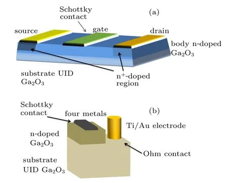
Fig.1. Schematic structure of (a) Ga2O3 MESFET in Ref. [11], and (b)Ga2O3 SBDs in Ref.[12]. UID:unintentionally doped.
In the Ga2O3MESFET,the work function is determined to be 5.23 eV in the gate material Ti/Au.[11]In Ga2O3SBD,four different metals(Pd,Ni,Pt,and Au)are used in the Schottky contact. Different metal has different work function.[12]In this calibration process, the carrier lifetime and the trap energy level are tuned to fit the experimental data. From formula(1),the minority carrier lifetime TAUP0 is more critical than TAUN0, since n ≫p in n-Ga2O3. Also, ETRAP will greatly influence the recombination rate since it appears in the exponential index. The TAUP0 value is fitted between 10−8s and 10−9s, and slightly different between two experiments.This value is similar to that in GaN. The n-type trap energy level is about 0.4 eV.
Figure 2 below shows the comparison between simulation results and the experimental data. The scale is suitably converted to make the plot placed in the same graph.
From Fig.2, we can see that the difference between currents from the experiment and the simulation is minimal.Therefore, our parameters and models for Ga2O3are reasonable, based on which we can proceed to design new Ga2O3structures.
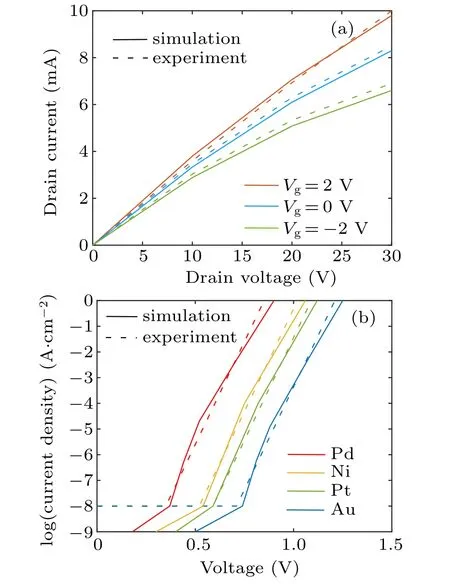
Fig.2. Comparisons between currents from experiment and simulation for(a)Ga2O3 MESFET and(b)Ga2O3 SBD.
4. Design of Ga2O3 on GaN SBDs
There are lots of researches on the GaN SBD,[17–19]and Ga2O3SBDs have attracted much attention recently.[20]In Ref. [20], the recent progress in the Ga2O3SBD is reviewed and some methods are provided to improve the Ga2O3SBD performance. These methods include increasing the doping concentration and using a p-Cu2O layer. Here, we propose another strategy and design a new structure of the Schottky barrier diode, which is the n-type gallium oxide on an unintentionally doped gallium–nitride substrate.The metal contact is defined as titanium and gold(Fig.3(a)). Following a similar procedure to the procedure shown later,we simulate the turnon current behavior and compare it with the result obtained in the case of using the Ga2O3substrate. Moreover, we change the gate length and the doping concentration to find the current trend(see Fig.3).
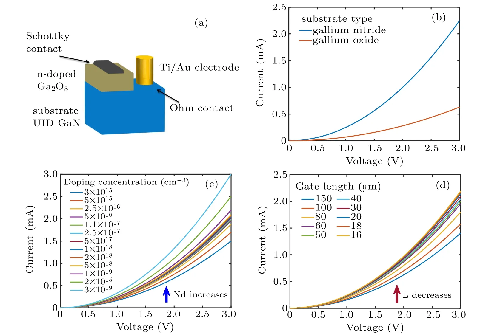
Fig.3. (a)Structure,variations of turn-on current with voltage for using(b)GaN substrate and Ga2O3 substrate,(c)different doping concentrations,and(d)different gate lengths,of gallium oxide on gallium–nitride substrate SBD.
From Fig.3(b) we can see that the current increases by three times after changing the substrate, which is good for application since the small current is difficult to detect. Figures 3(c) and 3(d) show the changing trend of current for different doping concentrations and the gate lengths, respectively. The n-type Ga2O3doping concentration changes from 3×1015cm−3to 3×1019cm−3. The current grows steadily at first,but increases rapidly when it is above 1×1019cm−3.The gate length is varied between 16µm and 150µm,and the current changes as expected.
An essential problem in the real application is the lattice mismatch in the epitaxy process.Gallium oxide is monoclinic,while gallium nitride is hexagonal. It is hard to grow gallium oxide on gallium nitride directly. An important strategy to solve this problem is to add a transition layer.[21]Here, we add a zinc oxide(ZnO)layer as a transition layer in between.Zinc oxide is a perfect transition layer since zinc oxide is also hexagonal so that it can be grown on the gallium–nitride substrate. Moreover, zinc oxide can form a solid solution with gallium oxide,[22]and it is feasible to stack a layer of gallium oxide on it. In the real molecule beam epitaxy(MBE)process,we can use Ga, Zn, and O atoms, and block the Ga source first. After some time, we open the Ga source and block the Zn source. We may have a ZnO–Ga2O3solid solution,and it is more feasible than stacking Ga2O3directly since Ga2O3and GaN have different lattice types.
Figure 4(a)shows the updated structure.After adding this new layer, the current decreases, but it is still larger than the current in the original Ga2O3on Ga2O3SBD(see Fig.4(b)).

Fig.4. (a) Structure of SBD after adding transition layer, and breakdown behaviors for (b) different substrates and (c) different structures of SBD.
Another important property of the SBD is the breakdown voltage. Here,our definition of breakdown voltage is the same as that of the GaN SBD breakdown voltage in Ref.[23],which corresponds to the voltage where the current suddenly drops or rises. Generally speaking, a Ga2O3device has a larger breakdown voltage than a GaN device, so this new structure should have a larger breakdown voltage than GaN SBD,which is confirmed through further simulating the breakdown behavior. After adding a transition layer,the breakdown voltage decreases,but it is still better than GaN SBD(see Fig.4(c)).
In summary, the design of adding a ZnO transition layer is successful. Its advantage is still over the original designs,though it is not so good as that without the transition layer. To make the device easily fabricated in experiment, this price is acceptable.
5. Conclusions
We designed a gallium oxide on gallium–nitride substrate SBD in this paper by TCAD simulations. We started this design by defining the new material Ga2O3in the software database since Ga2O3is not included in the material library.After that,the calibration simulation shows that our new definition accords well with the experiment data in Ga2O3MESFET and Ga2O3substrate SBD.We proceeded with this simulation and designed a new Ga2O3on GaN substrate SBD.This new SBD has a better turn-on property and a higher breakdown voltage than the original SBD. To solve the lattice mismatch problem in real fabrication, we added a transition layer ZnO.More simulations show that the SBD still maintains these good properties after adding this transition layer. Our simulation is the first systematic simulation of Ga2O3,which is of great significance for further conducting simulations.
Acknowledgment
We would like to thank our colleagues for their useful discussion with Dr. Fanming Zeng and Weichih Cheng from the School of Microelectronics, Southern University of Science and Technology, China and Teren Liu from the Department of Materials Engineering, University of British Columbia,Canada.

- Chinese Physics B的其它文章
- Novel traveling wave solutions and stability analysis of perturbed Kaup–Newell Schr¨odinger dynamical model and its applications∗
- A local refinement purely meshless scheme for time fractional nonlinear Schr¨odinger equation in irregular geometry region∗
- Coherent-driving-assisted quantum speedup in Markovian channels∗
- Quantifying entanglement in terms of an operational way∗
- Tunable ponderomotive squeezing in an optomechanical system with two coupled resonators∗
- State transfer on two-fold Cayley trees via quantum walks∗