
Neutron-induced single event upset simulation in Geant4 for three-dimensional die-stacked SRAM∗
2021-03-19 03:21LiHuaMo莫莉华BingYe叶兵JieLiu刘杰JieLuo罗捷YouMeiSun孙友梅ChangCai蔡畅DongQingLi李东青PeiXiongZhao赵培雄andZeHe贺泽
Chinese Physics B 2021年3期
Li-Hua Mo(莫莉华), Bing Ye(叶兵),†, Jie Liu(刘杰),‡, Jie Luo(罗捷), You-Mei Sun(孙友梅),Chang Cai(蔡畅), Dong-Qing Li(李东青), Pei-Xiong Zhao(赵培雄), and Ze He(贺泽)
1Institute of Modern Physics,Chinese Academy of Sciences,Lanzhou 730000,China 2University of Chinese Academy of Sciences,Beijing 100049,China
Keywords: neutron,three-dimension ICs,single event upset,multi-bit upset,Geant4
1. Introduction
The spacecraft avionics system is now becoming more and more miniaturized and highly integrated with the rapid development of the aerospace industry. The reliability requirements are facing more demanding conditions than ever before. There are various types of high-energy particles in space environment, which makes the spacecraft suffer the threat from single event effects(SEEs).Previously,heavy ions and protons are considered to be the main sources of SEE because of the high direct ionization energy and high flux,respectively. However, in commercial aerospace, earth orbit satellite,[1]Mars exploration,[2,3]and aviation,[4]the neutroninduced SEE has attracted much attention in recent years.
In 1979, Guenzer et al. first demonstrated single event upset(SEU)induced by neutrons in the laboratory.[5]In 1993,Olsen et al. reported function failures in new electronic equipment due to atmospheric neutrons SEU during regular intercontinental flights.[6]The impact of atmospheric neutrons on electronic devices became a relevant issue until Ziegler and Puchner suggested that cosmic rays were a long-lasting threat to electronic reliability in 2004.[7]SEU induced by neutrons is becoming a significant issue, especially for the advanced integrated circuits (ICs) with low-voltage and small feature size.[8-10]The three-dimensional integrated circuits (3D ICs)have higher integration, lighter weight, better electrical performance, less power consumption, lower profile and higher throughput than the planar ICs.[11,12]Therefore, it is increasingly favored in aerospace,aviation,and ground applications.The SEE sensitivity of 3D ICs is also a major concern for the field of radiation-hardened design.[13,14]Previous studies have shown that the shielding effect of 3D ICs can reduce the sensitivity of radiation effects caused by heavy ion and proton incidence.[15,16]As is well known, neutrons are more penetrating in 3D devices,and the study of neutron-induced SEE is necessary.
In this paper, a three-layer die-stacked device is constructed and investigated by using the Geant4[17]simulation tool based on a real planar device. The SEU sensitivity of the 3D SRAM caused by neutrons in an energy range from 1 MeV to 1000 MeV is studied.
2. Simulation setup
To verify the correction of simulation, a cuboid(12.5µm×25µm×25.9µm)device model which contained multi-layers was constructed in Geant4.10.04 as illustrated in Fig.1. The detailed layer information of the device model is shown in Fig.1(a). The SEU threshold linear energy transfer (LETth) is set to be 0.13 MeV/(mg/cm2) according to Ref. [18]. A critical charge (Qc) is defined as a minimum charge collection needed to cause an SEU. The value of Qcis mainly determined by the nodal capacitance.[19]If the collected charge in the sensitive volume(SV)is greater than the Qc,the SEU will occur. The Qcin unit of fC can be calculated from the following formula:
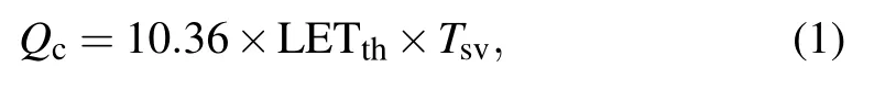
where LETthis in unit of MeV/(mg/cm2)and Tsvis the thickness of SV in unit ofµm.
Then, a nested SV array was constructed and calibrated according to Ref. [20]. As shown in Fig.1(b),the size of nested volume increases from SV1 (0.2 µm×0.19 µm×0.1 µm) to SV4 (3.5 µm×3.5 µm×0.45 µm),while the effective charge-collection efficiency decreases from SV1 to SV4. The SV1 only considers the most sensitive drain region for the off-state transistor. Thus,the corresponding charge-collection efficiency, α1, is set to be 100%. Besides,the thickness of SV1(0.1µm)is smaller than the depth of the well (0.45 µm) for the 65-nm technology.[21]Charge collection efficiency for SV2, SV3, and SV4 were set to be 0.130, 0.025, and 0.0075, respectively. Beyond the SV1 region, charges are collected from funneling area. The charge collection increases in the region out of the SV1 with the LET increasing. While ions striking,due to small LET,and smaller radius of delta electron diffusion,the SV1 is the major charge collection region.

Fig.1. (a)Single-layer die SRAM model used in Geant4 simulations. (b)Cross-section view of nested SV.Not drawn to scale.

Fig.2. SEU cross-section for experiments and Geant4 simulations versus LET.The experimental data are cited from Ref.[18].
Finally, the SEU cross-section is simulated as a function of incident heavy ion LETs as shown in Fig.2. The incident neutrons cannot induce SEE directly. The SEE is caused by secondary heavy ions,which are generated by the nuclear reactions between incident neutrons and nucleus of device materials, for instance Si, Cu, etc. Therefore, the accuracy of the simulated model can be verified by comparing the simulated results with the experimental results based on heavy ions.The simulation results obtained from the nested SV model are mostly consistent with experimental results as shown in Fig.2.
The results in Fig.2 verify the correctness of the simulation method. To simplify calculation and enhance operability, in this work only SV1 is considered as a sensitive volume in the subsequent studies of neutron-induced SEU. For 3D device simulation, a three-layer die-stacked device based on the above-mentioned planar device is built to study the neutron SEU sensitivity of 3D device. The 3D stacked model for Geant4 simulation in this work is presented in Fig.3. The size of the model cube is 12.5µm×25.0µm×23.7µm,and each die includes 25×25 SRAM cells and a 2.0-µm-thick silicon inter-strata layer. The first and the second layer die are bonded back to face structure, and the third layer die is boned back to back structure with the second layer die. The setting of the threshold LET is the same as the one in the single-layer SRAM model described above. The value of Qcin our simulation is 0.135 fC corresponding to 0.1-µm Tsv. Each cell corresponds to a unique number, and the energy deposited in each SV is recorded for every event. The number of incident neutrons for each simulation is 7×10⁸and the energy is in a range from 1 MeV to 1000 MeV.
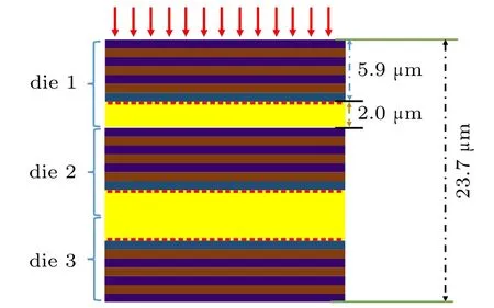
Fig.3. Simulation model of 3D die-stacked SRAM.Die 1 and die 2 are bonded back to face structure,and die 3 is back to back boned to die 2.Not drawn to scale.
3. Simulation results
The SEU cross-section (σ) in unit of cm2/bit in 3D diestacked SRAM is calculated from the following equation:
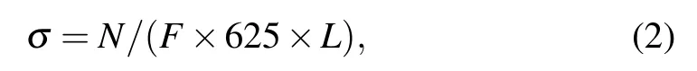
where N is the number of recorded upsets in each simulation,F is the total fluence of the neutrons in unit of neutrons/cm2,and L is the number of die layers of the device. The L=1 refers to the single-layer die device and L=3 refers to the whole three-layer die-stacked device model.
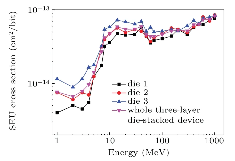
Fig.4. Neutron-induced SEU cross-sections versus neutron energy for three-layer die-stacked SRAM device model.
The trends for the SEU cross-sections in different dies and the overall 3D device with increasing energy of the incident neutrons are consistent. As the energy of incident neutrons increases,the SEU cross-section of the 3D almost keeps constant in an energy range from 1 MeV to 4 MeV and then increases sharply, reaching 5.88×10⁻¹⁴cm2/bit for 14-MeV neutron,which is about an order of magnitude higher than that for 1-MeV neutron. As incident neutron energy continues to increase, the SEU cross-section decreases at about 50 MeV,reaching 4.62×10⁻¹⁴cm2/bit for 100-MeV neutron and then increasing again.The SEU cross-section reaches its maximum value of 8.17×10⁻¹⁴cm2/bit,at 1000 MeV.
The nuclear reaction cross-sections and the characteristics (energy, species, etc.) of the secondary ions are the key parameters to analyze the neutron SEU. As illustrated in Ref. [22], the total nuclear reaction cross-section of neutronsilicon at 14 MeV is about a factor of 1.8 higher than that at 100 MeV, which means that the nuclear reactions are more probable at 14 MeV than at 100 MeV.On the other hand,the number of reaction channel strongly depends on the energy of incident neutrons, which greatly affect the characteristic (energy and ion species) of the secondary ions. As the energy increases, a larger number of reaction channels are open and more species of secondary ion are created. To understand the energy dependence, we analyze the secondary ions produced by neutron interactions with silicon at four neutron energy values (4 MeV, 14 MeV, 100 MeV, and 500 MeV), which will discussed in the next section.
In addition, as shown in Fig.4, the interesting point is that the neutron SEU cross-sections of different dies are different from that of heavy ions or protons. For low energy heavy ion and proton incident in a 3D stacked structure device, the SEU cross-section is vulnerable to being affected by the projected range.[16,23]As illustrated in Ref.[16],the SEU occurs only in the top layer die of the 3D device, when the primary proton energy is less than 0.8 MeV. But for neutrons, the result is entirely different due to its strong penetrating ability.The SEU cross-section value for the die farthest from the device surface is always highest,regardless of the incident neutron energy. And the discrepancies in the SEU cross-section among the three dies decrease as the incident neutron energy increases.
4. Analysis and discussion
4.1. Influence of LET threshold and the thickness of SV
The value of Qcfor a given circuit is a certain value,mainly determined by the nodal capacitance.[20]The critical charge changes with the circuit layouts and working conditions.[24-27]In Geant4 simulation, it is meaningful to study the influence of Qcon SEU by changing the LETthand the thickness of SV.[28-30]The SEU cross-sections of the whole three-layer die-stacked device versus neutron energy for different LET thresholds are shown in Fig.5, and the results for different thickness values of SV (0.1, 0.3, and 1.0 µm)are shown in Fig.6. These results are based on the model as shown in Fig.3. The model parameters differ in the LETthand thickness of the SV, respectively in Figs. 5 and 6. It is seen that the SEU cross-sections are dependent on the LETthand Tsv. Moreover, the SEU cross-section exhibits an increasing trend with the decrease of LETth. A similar trend is observed with the increase in Tsv. In the case of the particles with low LET, such as alphas or protons, the deposited charges in SV may exceed the critical charge as the LETthdecreases. The track length of secondary particles will increase with thickness of SV increasing while the deposited charges can exceed the critical charge.
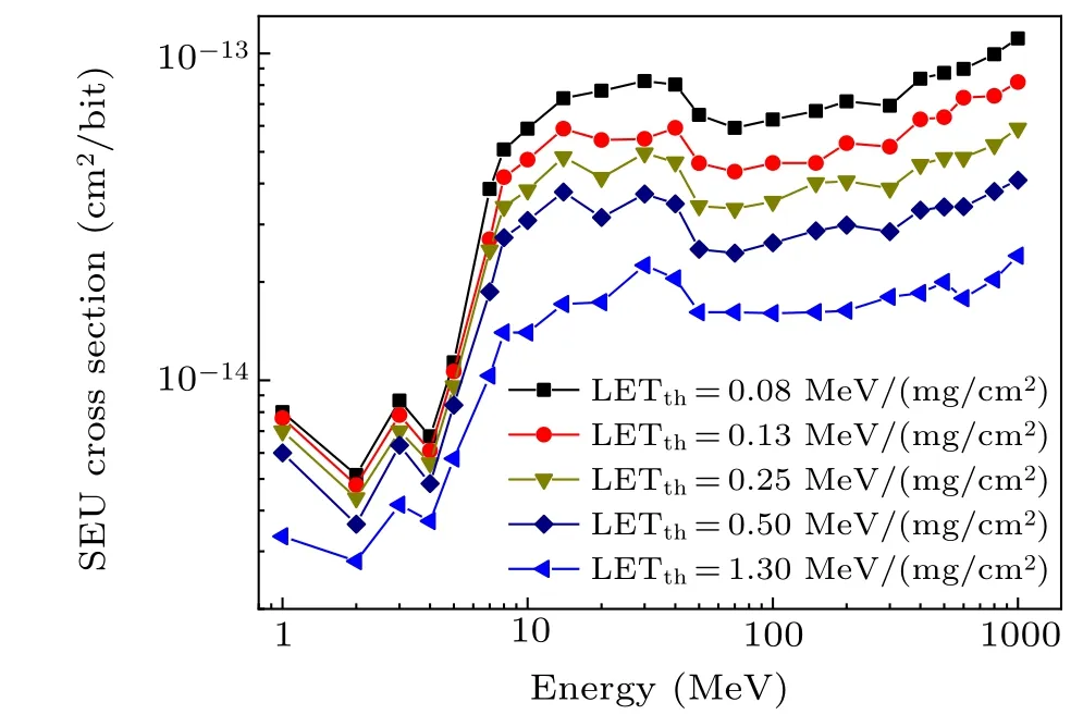
Fig.5. Neutron-induced SEU cross-sections of the whole three-layer diestacked device versus neutron energy for different LET thresholds.
To intuitively see the influences of the energy on the SEU cross-sections of different dies of the three-layer die-stack device, the results of incidence neutron with 4, 14, 100, and 500 MeV are analyzed as shown in Fig.7. The SEU crosssections for three dies all exhibit a decreasing trend with the increase of LETth. The discrepancy in the SEU cross section among the three dies keeps constant,though the critical charge changes. In addition,the SEU cross-section between die 1 and die 2 seems to have a few differences and to be unaffected by energy or LET threshold. The different factor of SEU crosssections between die 1 and die 3 is about four at 4 MeV of incident neutron, while it decreases with the energy increasing.It can be speculated that there are few differences among the SEU cross-sections of three dies as incident neutrons energy reaches higher than 500 MeV.It is due to the energy deposited along the neutron and secondary ion’s track.
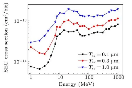
Fig.6. Neutron-induced SEU cross-sections of the whole three-layer diestacked device versus the neutron energy for different thickness values of the SV.

Fig.7. Neutron-induced SEU cross-sections of three dies versus critical charge for(a)4 MeV,(b)14 MeV,(c)100 MeV,and(d)500 MeV.
4.2. Charge deposited in SVs and secondary products
The occurrence of SEU directly depends on the quantity of charge deposited in the SV. Figure 8 shows the probability of charges deposited in SVs of different dies for various values of incident energy. It can be seen that neutrons with higher energy can deposit a larger quantity of charges in SVs. The maximum charge deposited in SVs can reach 77 fC for a single incident neutron with an energy of 500 MeV as shown in Fig.8(d). The probability distributions of the charge deposited in SVs of the three dies tend to be consistent with those as incident energy increases.
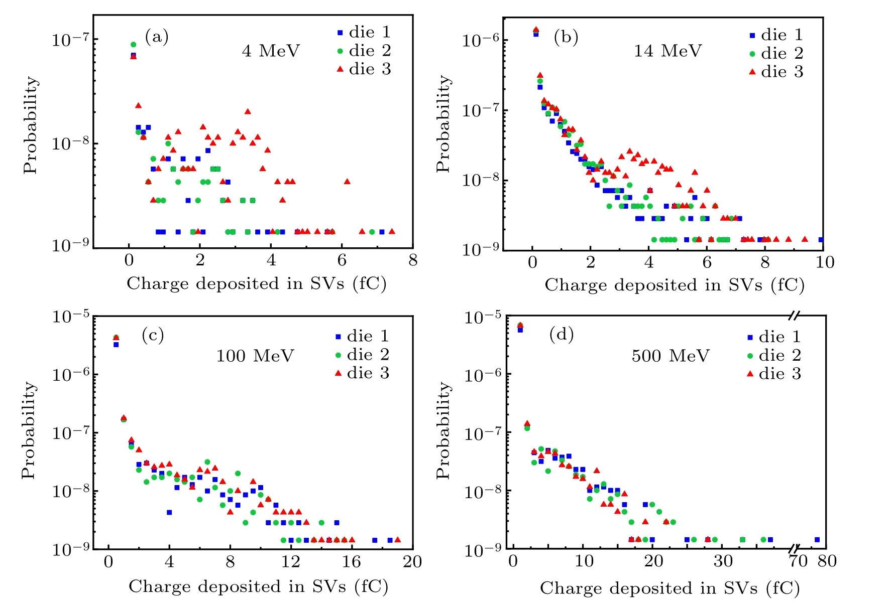
Fig.8. Variations of probability of charges deposited in SVs of three dies for neutrons with energy of (a) 4 MeV, (b) 14 MeV, (c) 100 MeV, and (d)500 MeV.

Fig.9. Variations of probability of collecting nuclides in the SV with atomic number for three dies at incident neutron energy of(a)4 MeV,(b)14 MeV,(c)100 MeV,and(d)500 MeV.
The SEU cannot be directly caused by neutrons, but by the secondary ions produced by neutrons interacting with the nuclei of device materials. Figure 9 shows the variation of possibility of secondary particles collected in SVs with atomic number for each die.Incident neutrons generate these nuclides in the 3D device with energy 4 MeV,14 MeV,100 MeV,and 500 MeV,respectively. The distribution of nuclides extends as the energy increases,which means that higher energy neutron irradiation results in a broader spectrum of nuclides. The silicon ion recoils induced by 4-MeV neutrons are the dominant contribution to SEU. The species of secondary ion collected in the SV of die 3 is least, but its total quantity is the largest in the three dies. It means that die 3 has the highest potential to induce SEU through secondary heavy ions. The total numbers of secondary ions of the three dies are ordered as die 3 >die 2 >die 1,which is corresponding to the sequence of SEU cross-section for every die.
The species of secondary ions is related to the number of reaction channels, which is greatly affected by the energy of incident neutrons. As shown in Ref.[31], the secondary ions from the n+Si reaction include proton,alpha,Li,Be,B,C,N,O, F, Ne, Na, Mg, Al, Si, and P, whose atomic numbers are less than sixteen. However, the atomic number of secondary ions collected in SVs are greater than fifteen, which is a significant difference. For die 1 and die 2,incident neutrons first pass through the layer of metallization and then reach the SVs.Some secondary ions, like Sc, V,Cr, Mn, and Fe, are created by the nuclear reactions between the neutrons and Cu; while Ta is produced by n+W reaction. Though most secondary ions are striking in the forward direction,the projected range is limited to their energy. Most of these heavier ions collected in die 1 and die 2 do not continue to reach die 3. Additionally, the die 3 is boned back to back to die 2. The incident neutrons first pass through the silicon layer,and then reach the layers of metallization,which leads most of secondary ions collected in the SVs of die 3 to have atomic numbers less than 15. Thus,in die 3, secondary ions mainly come from the nuclear reaction products of n+Si reaction. It indicates that the structure of die-stacked affects the SEU of 3D die-stacked devices and the light reaction products are the predominant contribution to SEU.
4.3. MBU
The energetic secondary particles can pass through the SVs in any direction to cause more than one bit upset. Though the energy of incident neutrons is only 2 MeV,we find several multiple-bit upsets(MBUs)after an irradiation of 7×10⁸incident neutrons. As shown in Fig.10(a),the counts of the MBU of the whole three-layer die-stacked 3D SRAM vary with the energy of the incident neutrons. The black,red,and blue histograms correspond to the MBU of double-bit upset (DBU),triple-bit upsets(TBU),and more than or equal to quadruplebit upsets(QDBU),respectively. Only several DBU events are observed when incident neutrons have 2 MeV and 5 MeV in energy. However,the counts of MBU clearly increase with the increase of neutron energy,and the DBU is a major contribution. In addition, high energy neutrons cause the majority of the high-multiplicity MBU events,as well as the high-chargecollection events shown in Fig.8. Although the SEU crosssections of incident neutron energy at 14 MeV,500 MeV,and 1000 MeV are almost equal, the MBU counts vary with neutron energy and differ greatly. These MBU events are related to the secondary ion species.
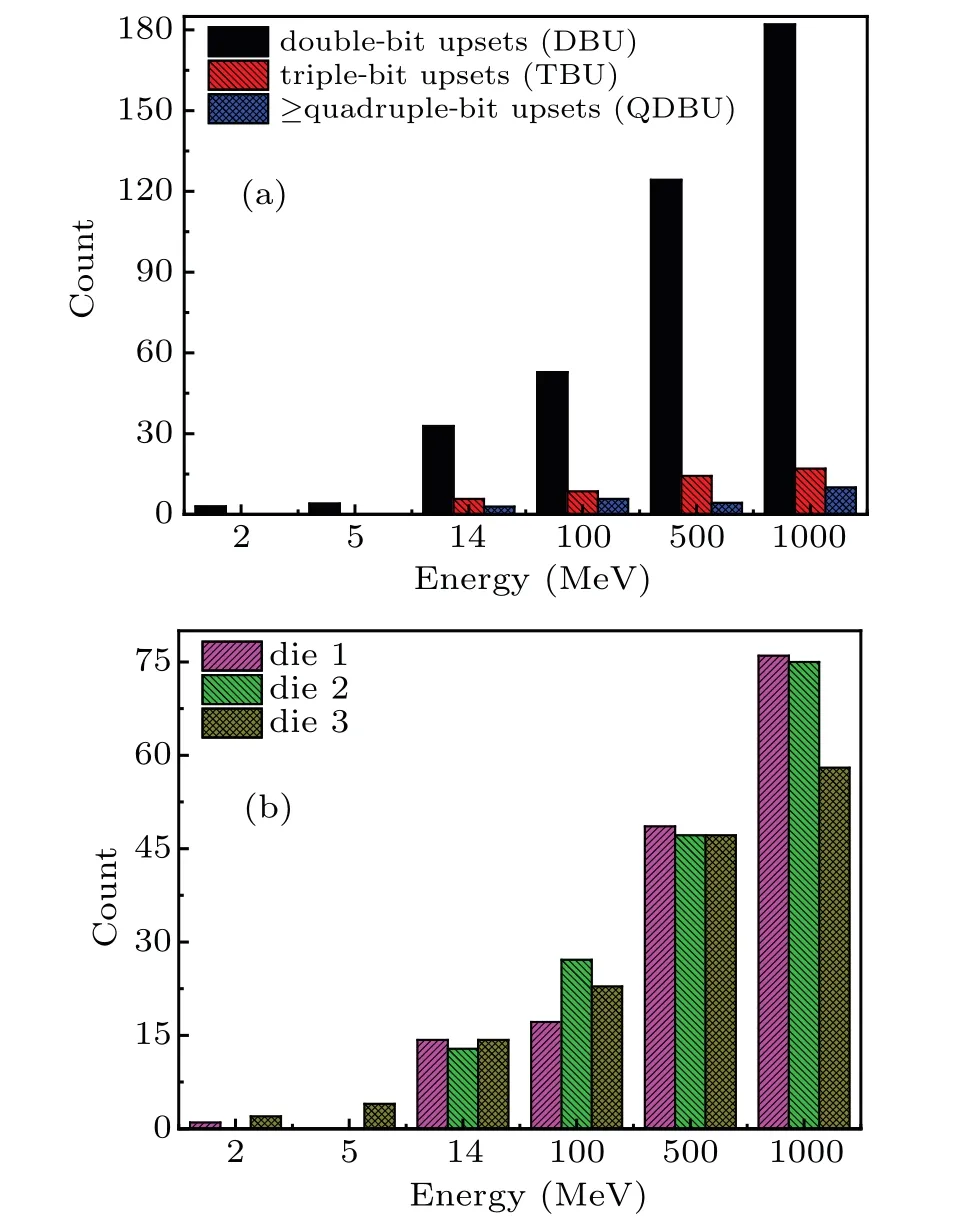
Fig.10. Histogram of count of MBU versus neutron energy in 3D SRAM for(a)the whole three-layer die-stacked and(b)different layer dies.
The analysis of the MBU events induced by 14-MeV neutrons reveals that the alpha particles produced in neutronsilicon reactions are the dominant contributors to MBU events.For incident neutrons with energy less than 14 MeV,the MBU count in die 3 is larger than in die 1 and die 2 as shown in Fig.10(b). However,this trend is not continuously applicable for high energy neutrons. The contribution of secondary particles produced by the nuclear reaction between the neutron and tungsten or other material of the metalized layer cannot be neglected when the incident energy is equal to or greater than 100 MeV as shown in Figs.9(c)and 9(d).
To further understand the mechanism by which the MBU occurs in each of the dies, we also analyze all the MBU patterns occurring in each of the three dies corresponding to the incident neutron energy of 14 MeV and 100 MeV.The MBU pattern on the whole three-layer die-stacked is significantly more complex than that on the single-layer die. As shown in Fig.11, there are more MBU patterns for 100-MeV neutrons than those for 14-MeV neutrons. An analysis of the secondary particles produced by 14-MeV neutrons reveals that all the MBU patterns in the whole three-layer die-stacked are caused by proton, alpha, Mg-24, and C-13. In addition, the MBU, except for DBU, is caused by the alpha particle in the energy range of 4.0 MeV-7.5 MeV.It is worth noting that an MBU is possibly induced by two secondary particles that are simultaneously produced by one neutron event. For example,the first pattern in die 1 in Fig.11(a) shows that the two bits constituting DBU are too far apart,which is induced by C-13 and alpha. Most of the MBU events are caused by secondary particles that traverse the SVs at grazing angles. In Fig.11(a),the maximum upset number is five,occurring in die 3,caused by an alpha particle with initial energy of 7.5 MeV. The direction in which the alpha particle traverses the SVs is nearly vertical to the direction of incident neutrons.
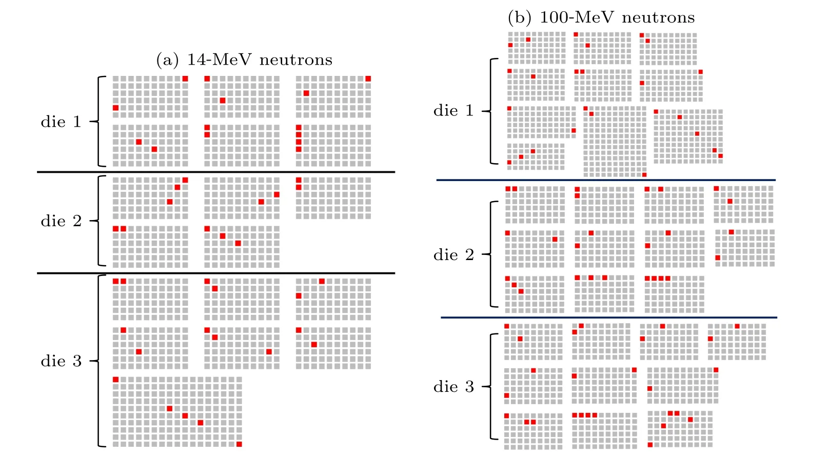
Fig.11. MBU patterns for(a)14-MeV neutrons and(b)100-MeV neutrons in each die of 3D die-stacked SRAM,with red square denoting upset cell,and gray square representing normal cell.
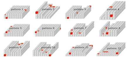
Fig.12. Patterns of TBU composed of bit upsets in different-layer dies in 3D die-stacked SRAM, with red box denoting upset cell, and gray box representing the normal cell.
The kinds of MBU patterns induced by 100-MeV neutrons are more complicated as shown in Fig.11(b). Most of the MBUs are also caused by alpha particles, and the maximum upset number is five in die 3. However, in die 1, we find that a five-bit upset is induced jointly by the Na-22 and the protons. The one-bit upset is induced by the secondary particles of Na-22. The other four-bit upset is induced by lowenergy protons with an initial energy of 2.89 MeV.As shown in Fig.9, protons are the main component of the secondary ion. The SEU induced by the direct ionization of low-energy protons cannot be ignored either.
Moreover, for 1000-MeV neutrons, we observe that the maximum upset number is ten-bit upset number caused by Al-29 in die 2. It is noted that the TBU or more-bit upset is composed of the bit upsets in different dies that occur when the neutron incident energy is beyond 1000 MeV. This phenomenon is not observed for incident neutrons with lower than 500 MeV in energy. Since the probability of this event happening is small, only twelve events are observed in 7×10⁸incidents. The TBU and other patterns greater than or equal to QDBU composed of the bit upsets in different dies are shown in Fig.12. Some happen in three-layer dies simultaneously,such as, pattern 1, pattern 2, pattern 3, and pattern 4. The others occur simultaneously in two-layer dies. Most of these MBUs are caused by more than one secondary particle induced by the same incident event. The variety and complexity of the MBU pattern of the whole three-layer die-stacked increase with the neutron energy increasing.
5. Conclusions
Simulation of neutron irradiation in a 3D die-stacked SRAM is performed using the Geant4 tool. The results indicate that the SEU cross-section strongly depends on the incident neutron energy,which increases as the incident neutron energy increases. The SEU cross-sections of the incident neutrons with energy of 14 MeV,500 MeV,and 1000 MeV are of the same order of magnitude, which are one order of magnitude higher than those of the neutrons with low energy ranging from 1 MeV to 4 MeV.die 3 has a higher upset cross-section than die 1 and die 2 obviously when the neutron energy is less than 14 MeV.The gaps in the SEU cross-section between the three dies decrease as the neutron energy increases. One reason for this difference is due to the structure of die-stacked,which results in the different secondary particles being produced in the different layer-dies. The other reason is due to the fact that the secondary particles created in die 1 and die 2 by high energy neutrons have the potential to move forward and induce the SEU in die 3 due to their long projected range.
The MBU count increases as the neutron energy increases and the DBU is the dominant type of MBU.When the incident neutron energy is less than 14 MeV,the MBU counts in die 3 is larger than those in die 1 and die 2. The number of MBU occurring in die 1 and in die 2 are both larger than that in die 3 as the incident neutron energy increases. This is due to the contribution of the increasing secondary particle created by the nuclear reaction between neutrons and the metallization material. An analysis of the MBU reveals that the differences in MBU pattern between the three dies are not significant. However, the variability in the MBU pattern will increase as the incident neutron energy increases.
猜你喜欢
Chinese Physics B(2022年11期)2022-11-21
Chinese Physics B(2022年9期)2022-09-24
湘潮(上半月)(2022年3期)2022-09-13
Chinese Physics B(2022年5期)2022-05-16
湘潮(2021年3期)2021-09-05
湘潮(上半月)(2021年3期)2021-07-20
时代邮刊(2019年9期)2019-05-21
美与时代·美术学刊(2018年10期)2018-01-25
汉语世界(2017年5期)2017-09-21
湘潮(2017年4期)2017-06-05
- Chinese Physics B的其它文章
- Transport property of inhomogeneous strained graphene∗
- Beam steering characteristics in high-power quantum-cascade lasers emitting at ~4.6µm∗
- Multi-scale molecular dynamics simulations and applications on mechanosensitive proteins of integrins∗
- Enhanced spin-orbit torque efficiency in Pt100−xNix alloy based magnetic bilayer∗
- Soliton interactions and asymptotic state analysis in a discrete nonlocal nonlinear self-dual network equation of reverse-space type∗
- Discontinuous event-trigger scheme for global stabilization of state-dependent switching neural networks with communication delay∗