
Synaptic plasticity and classical conditioning mimicked in single indium-tungsten-oxide based neuromorphic transistor*
2021-05-24 02:23RuiLiu刘锐YongliHe何勇礼ShanshanJiang姜珊珊LiZhu朱力ChunshengChen陈春生YingZhu祝影andQingWan万青
Chinese Physics B 2021年5期
Rui Liu(刘锐), Yongli He(何勇礼), Shanshan Jiang(姜珊珊), Li Zhu(朱力),Chunsheng Chen(陈春生), Ying Zhu(祝影), and Qing Wan(万青)
School of Electronic Science and Engineering,Nanjing University,Nanjing 210023,China
Keywords: neuromorphic transistors,synaptic plasticity,oxide-based semiconductors,classical conditioning
1. Introduction
Human brain can process multi-dimensional information simultaneously because it is a parallel, plastic, and faulttolerant neural network with ~1011neurons and ~1015synapses.[1,2]Although advanced supercomputers based on silicon based CMOS integrated circuit can perform precise digital calculation very fast,the energy consumption and space occupation are enormous.[3,4]In order to deal with complicated and unstructured data efficiently, the concept of brainlike computing and neuromorphic system was proposed.[5]
In neuroscience, learning and memory are established on the change of synaptic weight between neurons.[6]According to various time scales, synaptic plasticity could be classified as short-term plasticity (STP) and long-term plasticity (LTP). STP is temporary change of synaptic weight which persists a few milliseconds or minutes. However,LTP will last for a few hours, or longer.[7]By enhancing or shortening synaptic strength, synaptic plasticity could be modified or transformed.[8–16]During the past decade, twoterminal devices, such as memristor, have been proposed to emulate biological synapses.[17–21]In addition,multi-terminal transistors have been also proposed for artificial synapse application.[22–32]With additional control gate electrodes providing pre-synaptic signal inputs,post-synaptic current can be read synchronously. By now, some synaptic functions, such as excitatory post-synaptic current(EPSC),paired-pulse facilitation (PPF), metaplasticity, spike timing dependent plasticity (STDP), have been successfully simulated. With a huge gate capacitance, electric-double-layer (EDL) transistors can operate at a very low voltage. Furthermore,electrostatic modulation and electrochemical process in electrolyte gated EDL transistors are very similar to the ionic modulation in biological synapses. Thus, these transistors have great value in neuromorphic systems.[9,10,28–30]
Associative learning plays an indispensable role in individual adaptability, and classical conditioning is a simple example.[33]A few reports been demonstrated the emulation of this behavior in new-concept electronic devices.[34–38]Although the classical conditioning could be successfully emulated by these devices, a complex circuit was usually employed in the experiment. Recently, a dual-gated synaptic transistor was used to mimic classical conditioning. Inputs applied on the topgate and bottomgate were regarded as the conditioned stimulus (CS) and unconditioned stimulus (US),respectively.[39]According to STDP learning rules, Zhu et al.[40]illustrated classical conditioning in an oxide-based neuromorphic transistor. US and CS were applied on drain electrode and gate, respectively. Especially, Yang et al.[41]and Chen et al.[42]took the advantage of different voltages on behalf of CS and US to investigate the classical conditioning on a memristor and a transistor,respectively.
Here,we fabricated indium-tungsten-oxide(IWO)-based neuromorphic transistors gated by proton conducting chitosan films. Some synaptic functions, such as EPSC, PPF, filtering, were emulated. Moreover, two types of STDP (Hebbian STDP, and anti-Hebbian STDP) and multistore memory(sensory memory, short-term memory, and long-term memory) were also emulated. At last, classical conditioning was successfully demonstrated. Such neuromorphic devices have potential application in neuromorphic systems.
2. Experimental details
Firstly,acetic acid(~2 wt%)is added into deionized water. Secondly, chitosan solution (~2 wt%) is prepared by dissolving chitosan powder into above solvent. Thirdly, chitosan solution is drop-coated onto the ITO glass substrates and put in ambient air to shape into homogeneous chitosan films. Next, patterned IWO films (980 µm × 1600 µm) are deposited on the chitosan films with a metal shadow mask by sputtering with a RF power of 100 W, an Ar flow rate of 28 sccm, and a working pressure of 0.5 Pa. The target material is IWO (In2O3: WO3= 99 : 1 in wt.%). Finally, patterned Ag drain/source electrodes are evaporated on the IWO films by vacuum thermal evaporation. The channel width(W)and length (L) are 1000 mm and 80 mm, respectively. The schematic diagram of the IWO-based neuromorphic transistor is shown in Fig. 1(a). The frequency dependent capacitance of the chitosan electrolyte film is characterized using the impedance analyzer(HIOKI IM 3533-01 LCR meter).Electrical performance of the IWO-based synaptic transistors is measured by source measurement units(Keithley 2636B).
3. Results and discussion
The specific capacitance curve of the chitosan film is shown in Fig.S1(a). An EDL capacitor can be formed due to the accumulation of proton at chitosan/metal electrode under an external field. A maximal specific gate capacitance value(Ci)of ~5.7µF/cm2can be measured at 1.0 Hz. Output plots and transfer characteristics are provided in Figs. S1(b) and S1(c), respectively. From these output plots, the devices exhibit a good ohmic contact at low Vds. Because of the mobile protons in the chitosan electrolyte, a counterclockwise hysteresis can be observed in the transfer curve, which is necessary for synaptic function emulation. The current on/off ratio of the IWO-based synaptic transistor is estimated to be~2.0×10⁶. Moreover,as shown in Fig.S1(d),the gate leakage current is measured to be as low as 2.0 nA. Here, the modulation of the IWO channel conductance should be explained. Under a positive gate voltage,proton in the chitosan film will migrate to the channel/chitosan interface. Such interfacial EDL modulation can modulate the IWO channel current at a low gate voltage range. Thanks to the mobile proton and interfacial EDL modulation,biological synaptic functions can be emulated in an IWO-based synaptic transistor. Here we should point that the properties of the oxide-based EDL transistors can be influenced by the humility,so in the future,device package should be done in order to control the humidity.Temperature can also influence the electrical properties of the oxide-based EDL transistors gated by electrolyte,our preliminary experimental results show that such device can operate safely in the temperature range of 0°C to 80°C. In fact, as a biological neural network system, our brain only works in a very narrow temperature range. So,function is the first and the temperature range is secondary. In the future, controlling the temperature for a small volume brain-like system should not be a big problem.

Fig.1. (a)A diagram of the IWO-based neuromorphic transistor. (b)A diagram showing the biological synapse structure.
As shown in Fig.1(b),a synapse consists of pre-synapse,cleft,and post-synapse,and biological signal can be transmitted from the pre-synapse to the post-synapse. Some investigations indicated that the synaptic plasticity could be tuned by neurotransmitters or ionic fluxes in the cleft while the action potential is triggered by the pre-synapse.[6,7,43]The operation principle of the IWO-based neuromorphic transistor is similar to the process of synaptic plasticity modulation. When a pre-synaptic spike is evoked, an EPSC in IWO channel will be measured with a small reading voltage applied between the source and drain electrode(Vds).
Figure 2(a)shows a classical EPSC response of our IWObased neuromorphic transistor. The pre-synaptic spike is(0.2 V, 20 ms) and the reading voltage (Vds) is 0.1 V. When the spike comes to the end, a max EPSC value of ~4.7 nA is measured. The EPSC curve increases quickly in response to the pre-synaptic spike and then decays to the initial level step by step. The movement of proton within chitosan film plays a significant role in triggering EPSC. When a positive pulse voltage is applied on the gate electrode, proton will accumulate at electrolyte/IWO interface. After the pre-synaptic spike, proton will migrate to the balanced position, and the current returns to the initial level.[10]The energy dissipation of a spike event can be calculated by W =Ipeak×t×Vds, where Ipeakand t are the peak value and pulse width, respectively.The energy consumption per spike is estimated to be ~9.4 pJ.Figure 2(b)shows the energy consumption with various pulse amplitudes. As Vgsreduces, the energy consumption will reduce. Moreover, the energy consumption is also influenced by reading voltage Vdsand spike duration. When the reading voltage is reduced to 0.01 V,the energy consumption can be reduced to ~0.5 pJ,and the corresponding EPSC curve is shown in Fig.S2. Such energy consumption is much less than that of the classical CMOS-based artificial synapse.[44]
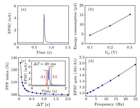
Fig. 2. (a) A post-synaptic current of the IWO-based synaptic transistor measured under a voltage spike (0.2 V, 20 ms). (b) Energy consumption changes with Vgs. (c) PPF index as a function of ΔT. (d) Spike frequency dependent EPSC gain.
As an important short-term plasticity, PPF is induced by 2 serial pulses with a short time interval (ΔT). Due to the successive release of neurotransmitters, the second spike response will be enhanced. PPF is widely considered to play a crucial role in temporal signal decoding.[7]In this work,PPF can be emulated in single IWO-based synaptic transistor.The inset in Fig. 2(c) is a response curve of PPF. The EPSC curves are evoked by two pre-synaptic spikes(0.2 V,20 ms)at ΔT =20 ms. As shown by the curve,the second EPSC peak is larger than the first one.As we all know,the movement of proton in chitosan takes some relaxation time. Considering ΔT is less than the relaxation time, some protons will not migrate back to their initial position. As a result, more protons will gather at the interface and the post-synaptic current in the IWO channel layer will also increase due to the corresponding field effect modulation. Figure 2(c)shows the PPF as a function of the interval time between two input spikes. A maximum PPF index of ~126 % is measured at ΔT =20 ms, and the PPF index decreases gradually when ΔT increases gradually.
Thanks to short-term synaptic facilitation, synapse can exhibit a high-pass filtering behavior. Such filtering is a primary operation which allows post-synaptic neurons to behaviorally perceive the relevant stimulus characteristics from presynaptic spike trains.[29,45]Based on the PPF features of the proposed IWO-based neuromorphic transistor,stronger synaptic responses can be observed when the high frequency presynaptic stimulus is applied on the gate electrode. Figure 2(d)shows the frequency dependent EPSC gain. Each spike train contains eight spikes (0.2 V, 20 ms). When the spike frequency increases, the EPSC gain (A8/A1) increases accordingly. Thus,a biological filtering is successfully emulated.
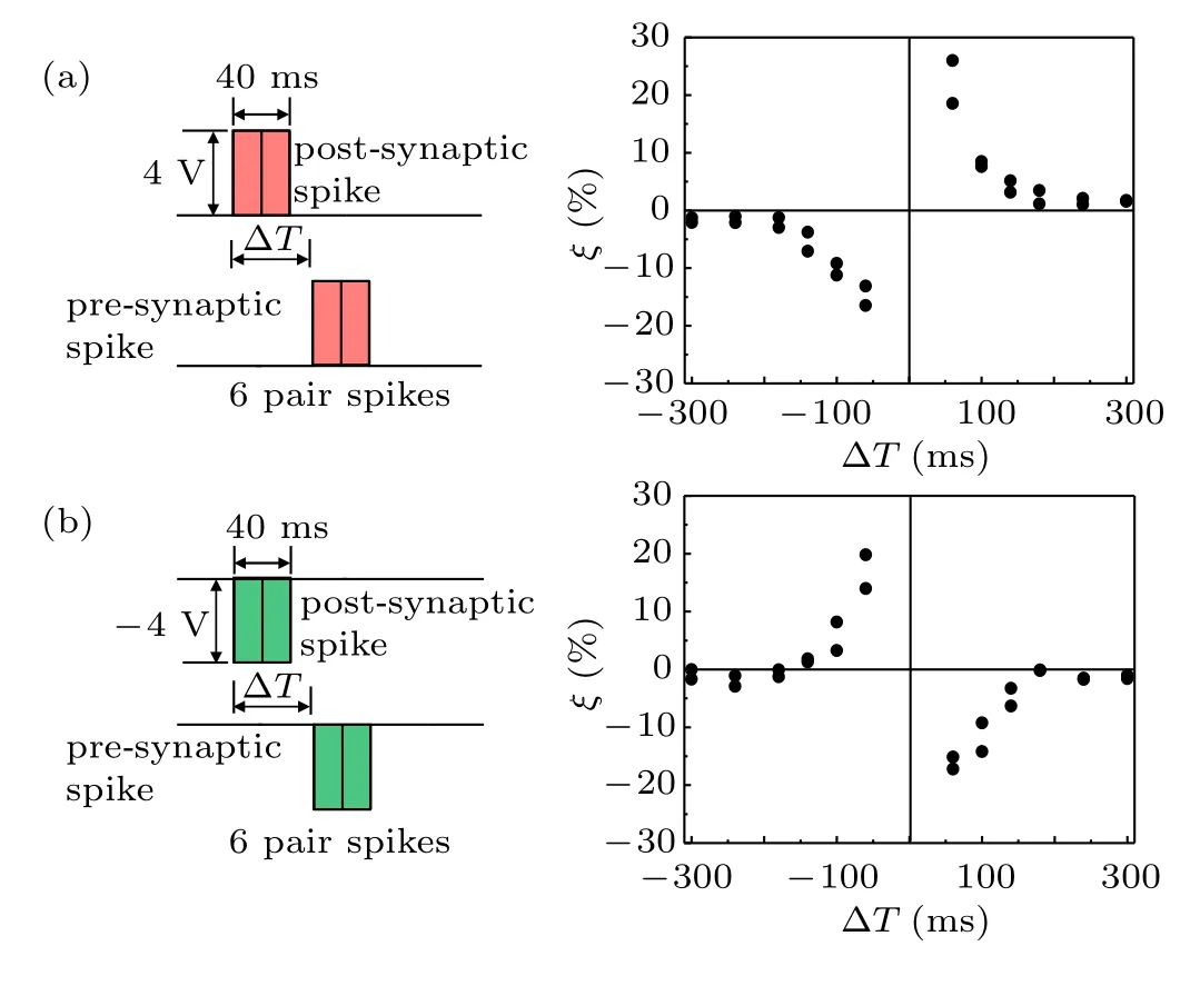
Fig.3. (a)Six pair of pre-synaptic and post-synaptic spikes adopted in Hebbian STDP test. (b)Measurements for anti-Hebbian STDP learning rule.
In neuroscience,long-term plasticity is believed to be the foundation for learning and memory.[46]STDP is an important kind of long-term plasticity, where the synaptic weight could be adjusted by intervals between pre-synaptic and postsynaptic spikes. It illustrates synaptic learning rules which changes conventional Hebbian synaptic plasticity,and plays a significant role in cognitive behavior.[46]Generally, there are two types of STDP, the symmetric and anti-symmetric Hebbian learning rules.[47]In typical STDP,when ΔT >0,the connection strength will be potentiated or depressed. However,when ΔT <0, the connection strength will be depressed or potentiated.[48]Here,these two types of Hebbian STDP learning rules can be emulated in our IWO-based synaptic transistor. Figure 3(a)shows 6 pair of pre-synaptic and post-synaptic spikes(4.0 V,40 ms)which are applied on the gate and drain electrodes,separately. A reading pulse(0.1 V,20 ms)is used to read the synaptic strength. The change of the synaptic plasticity can be written as

where W0is the original synaptic strength. The WSTDPis the synaptic strength after STDP measurement.[40]When ΔT >0,long-term potentiation will be formed. On the contrary,when ΔT <0, long-term depression can be formed. Anti-Hebbian STDP can also be realized by applying 6 pair of pre-synaptic and post-synaptic spikes(−4 V,40 ms)on gate and drain electrodes,respectively(Fig.3(b)).
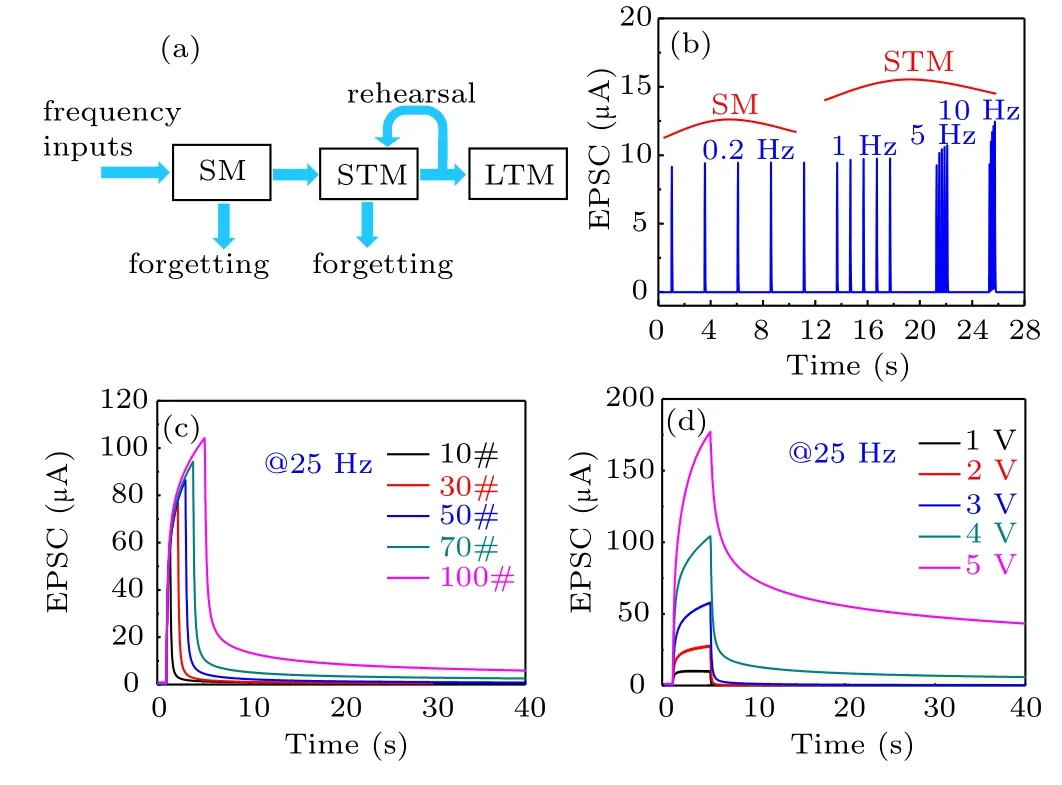
Fig. 4. (a) A diagram of the biological memory consolidation process.(b)SM and STM can be realized at low frequency inputs. (c)STM to LTM transition by increasing spike numbers. (d) STM to LTM transition by increasing spike amplitudes.
In biological,the transition of short-term memory(STM)to long-term memory(LTM)was thought as a major learning rule.[49]In 1968, Atkinson and Shiffrin put forward a multistore type of brain memory, as shown in Fig. 4(a).[50]This process illustrates 3 types of memory,sensory memory(SM),short-term memory, and long-term memory. By application of adequate stimulus, SM could transform into STM. Moreover, STM could transform into LTM, too. Frequency dependent EPSC responses are shown in Fig. 4(b). The voltage pulse (4.0 V, 20 ms) is used as repeated stimulus. First,five pre-synaptic spikes(0.2 Hz)are applied on the gate electrode to mimic SM. The peak EPSC values of ~9.0 µA can be observed and each EPSC decays back to the initial current.When applying pre-synaptic spikes with a frequency range from 1.0 Hz to 10 Hz,peak EPSC values will increase due to multi-pulse facilitation,like a series of PPF.However,EPSCs also decay to the initial current when the spikes end. These processes simulate the STM behaviors. Although 100 pulses(4.0 V,20 ms)at 10 Hz are applied on the gate electrode,EPSC will still decay to the original value,as shown in Fig.S3. The transition of LTM is mimicked at the frequency of 25 Hz,as illustrated in Figs.4(c)and 4(d). The EPSC responses with different pulse number under the same pre-synaptic spike(4.0 V,20 ms)are demonstrated in Fig.4(c). EPSC responses change with the variation of the pulse number. LTM can be obtained when the pulse number is larger than 70. In this case, EPSC will not decay back to the initial value. When the gate pulse number is very samll,proton in the chitosan film will migrated to the channel/chitosan interface and induce the accumulation of carriers. However,some protons will be penetrated into the IWO channel layer and cause electrochemical doping when the gate pulse number is large enough. As a result, the channel conductivity will be nonvolatile increased, and LTM can be observed. Some previous reports have already proved that proton permeation and electrochemical doping are the main mechanisms for STM to LTM transition.[35,51,52]STM also can be transformed into LTM by increasing the pre-synaptic spike amplitudes(Fig.4(d)). The pulse number and frequency are fixed at 100 pulses and 25 Hz,respectively. When the amplitude is above 4.0 V, the EPSC will not return to the initial level. Moreover, pulse width dependent synaptic plasticity is also investigated, as shown in Fig. S4. LTM can also be obtained when the pulse width is increased.

Fig. 5. Classical conditioning experiment. (a) Experimental arrangement and flow sheet for mimicking classical conditioning in an IWO-based synaptic transistor.(b)Similar Pavlovian process realized in an IWO-based synaptic transistor.Vgs of 3.0 V represents food while Vgs of 2.0 V represents bell.
Classical conditioning,namely,Pavlovian conditioned reflex, which could be acquired by applying a stimulus and an unconditional stimulus to an individual many times.[53]After associative learning, the individual can possess a capacity which induces conditioned responses like unconditional responses while applying the stimulus only. Four essential factors in this experiment are often utilized,unconditioned stimulus(US),unconditioned response(UR),conditioned stimulus(CS),and conditioned response(CR).During Pavlov’s dog experiment,feeding food and ringing bell are called US and CS,respectively. And the salivation caused by US is called UR.Before training,salivation only can be caused by feeding food(US).In the time of conditioning process,the dog was fed with food and ringing bell repeatedly. Thus, the relationship between CS and US is established. As a result,the salivation of the dog can be triggered by CS alone after training. That is to say that the CR is triggered.And the function of US is replaced by CS.It should be noted here that LTP plays an indispensable role in the process of associative learning. With the behavior of LTP, Pavlovian conditioning could be realized on our IWO-based transistors. In the experiment, the voltage pulse(2.0 V,20 ms)with a frequency of 0.5 Hz applied on the gate is considered to be‘ringing bell’(CS)while pre-synaptic spike(3.0 V,20 ms)with a frequency of 0.5 Hz applied on the gate is regarded as‘food’(US),as shown in Figs.5(a)and 5(b). And 1.0 µA of the synaptic weight is set as the threshold. Before conditioning process, 6 US and 6 CS are imposed separately on the gate. When US is applied only, the synaptic weight is over 1.0µA and the unconditioned response is caused. However,the synaptic weight is under threshold when applying CS alone. Then,100 bell stimuli(2 V,20 ms)and 100 food stimuli(3.0 V,20 ms)with a frequency of 25 Hz are utilized on the gate alternately as training spikes, as shown in Fig.5(b). After training, the synaptic weight is increased. In other words,the association behavior between CS and US is built. By application of CS alone, the synaptic weight is above 1.0 µA.That is to say, CS can trigger CR and conditioning reflex is realized. The features of classical conditioning also contain extinction. With the decay of synaptic weight, the salivation response decreases gradually. Conditioned responses will recover to its initial state after ~155 successive CS applying on gate solely,which indicates that the association learning is extinguished. Thus, the classical conditioning is successfully emulated in the IWO-based synaptic transistor.
4. Conclusion and perspectives
In summary, IWO-based EDL transistors gated by chitosan-based biopolymer electrolyte were fabricated and proposed for neuromorphic devices. Such multi-terminal neuromorphic devices show good electrical performance. Some basic synaptic functions, including EPSC, PPF, and filtering,were emulated in single IWO-based device. Hebbian STDP and anti-Hebbian STDP learning rules were also emulated by applying different spike protocols. Plasticity transition and classical conditioning were successfully emulated in single device, too. Our results indicate that IWO-based neuromorphic transistors have potential application for brain-like computing and neuromorphic systems.
- Chinese Physics B的其它文章
- Corrosion behavior of high-level waste container materials Ti and Ti–Pd alloy under long-term gamma irradiation in Beishan groundwater*
- Degradation of β-Ga2O3 Schottky barrier diode under swift heavy ion irradiation*
- Influence of temperature and alloying elements on the threshold displacement energies in concentrated Ni–Fe–Cr alloys*
- Cathodic shift of onset potential on TiO2 nanorod arrays with significantly enhanced visible light photoactivity via nitrogen/cobalt co-implantation*
- Review on ionization and quenching mechanisms of Trichel pulse*
- Thermally induced band hybridization in bilayer-bilayer MoS2/WS2 heterostructure∗