
Extended-source broken gate tunnel FET for improving direct current and analog/radio-frequency performance*
2021-07-30 07:43HuiFangXu许会芳WenSun孙雯andNaWang王娜
Chinese Physics B 2021年7期
关键词:王娜
Hui-Fang Xu(许会芳), Wen Sun(孙雯), and Na Wang(王娜)
Institute of Electrical and Electronic Engineering,Anhui Science and Technology University,Fengyang 233100,China
Keywords: extended-source,broken gate,radio-frequency performances,tunnel field-effect transistor
1. Introduction
As the size of metal-oxide-semiconductor field-effect transistors (MOSFETs) scales down continuously, the power dissipation, limitation of subthreshold swing (SS) of 60 mV/decade of current at room temperature, and significant increase of the off-state currentIoffhave become critical issues. However, in next-generation technology nodes,novel devices with low power, high on-chip packing density,and high speed are of great demands. Therefore,tunnel fieldeffect transistors(TFETs)have been proposed to replace conventional MOSFETs in order to overcome the shortcomings of MOSFETs. In contrast to the thermal injection of carriers for MOSFETs,the working mechanism of TFETs is bandto-band tunneling (BTBT).[1]The BTBT mechanism can reduce the values of SS, various researches have proved that SS is lower than 60 mV/decade at 300 K.[2-4]Moreover, the BTBT mechanism produces a large tunneling barrier for the current carriers when the device is operated in the off-state,which makesIoffsmaller. As a result, the power dissipation of TFETs is lower than that of MOSFETs. However,in spite of the above-mentioned advantages for TFETs, conventional TFETs suffer from ambipolar behavior and small on-state currentIon. Therefore,many papers have extensively boostedIonand reduced ambipolar behavior. For the purpose of suppressing ambipolar behavior, many technologies have been used, such as low doping levels in the drain region,[5]underlap and overlap of gate-drain.[6-8]Furthermore, in order to enhanceIon, many novel architectures of TFETs such as T-shape,[9,10]nanowire,[11,12]L-shape,[2,13]U-shape,[14]nanotube,[15,16]are proposed. Moreover, the materials with small energy bandgap,[17-19]high-kgate dielectrics,[20]high doping levels in the source region as well as abruptness at the source-channel tunnel junction are need to design. As is well known, the tunneling barrier decreases with the energy bandgap decreasing,so the tunneling rate increases,which results in a largeIon. Moreover,a sharp abrupt junction between the source region and channel region should be formed in order to increase the generation efficiency of BTBT as much as possible, and as a result,Ionis boosted. Thus, many researchers have concentrated on how to form an abrupt source-channel junction based on the process technology.
Furthermore, for better applications from the perspective of low-power and analog/rf circuits, the performance parameters of TFETs such as low SS, small threshold voltageVth, high on-state current to off-state current ratioIon/Ioff,large transconductancegm, high cut-off frequencyfT, high gain bandwidth product (GBP), and large transconductance frequency product (TFP) should be obtained. Miscellaneous techniques have been reported in the literature to improve the dc and analog/rf performance parameters.[21-28]Pujaet al.reported a ferroelectric TFET with SS of 40 mV/decade,Ion/Ioffof 8.4×10¹¹.[29]Tripureshet al.reported an extended-source double-gate TFET (ESDG TFET) withVthof 0.42 V, SS of 12.24 mV/decade,Ion/Ioffof 1012,fTof 37.7 GHz, GBP of 3.4 GHz.[30]Rounaket al.proposed a broken gate TFET(BG TEFT), which combines the advantages of the double gate TFET(DG TFET)and the L-shaped TFET(L TFET).[31]Moreover, superior characteristics such as small ambipolar current, low SS, and largeIonare achieved for BG TFET. In this paper,a novel TFET named as the ESBG TFET,which is an amalgamation between the ESDG TFET and the BG TFET in order to enhance the dc and analog/rf performance.
2. Device structure
The structure of the ESBG TFET is shown in Fig.1. The source region is extended into the channel for the purpose of enhancing the point and line tunneling probabilities at the tunneling junction.The gate dielectrics near the source region and near the drain region are hafnium dioxide(HfO2)and silicon dioxide (SiO2) in order to reduce ambipolarity. It should be noted that the device is called the ESBG TFET(HfO2)when the gate dielectrics near the source and drain regions are HfO2.Similarly,when the gate dielectrics are silicon dioxide(SiO2),the device is called the ESBG TFET (SiO2). The length and height of the p+source region isLsandTs,respectively. The silicon thicknesses near the gate and near the drain areT1andT2,respectively. The lengths of gate and gate 2 areL1andL3,respectively. The distance between gate and gate 2 isL2. The parameters for the ESBG TFET are listed in Table 1.
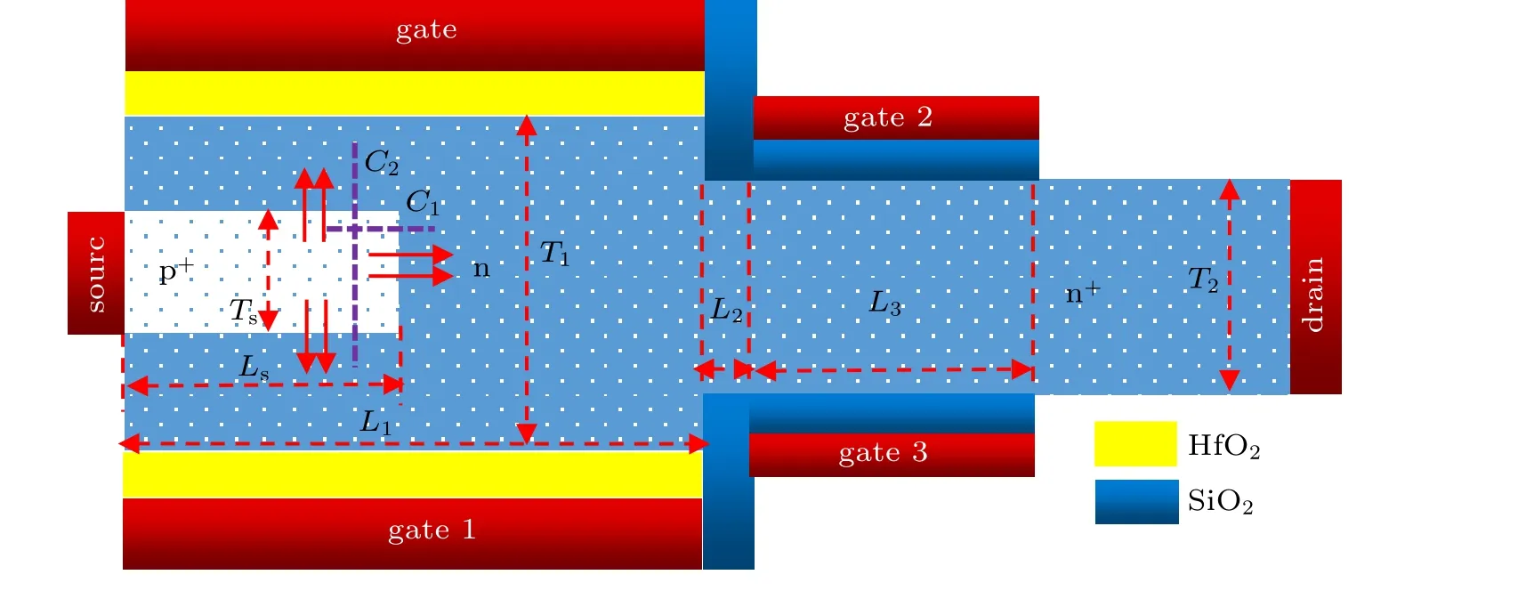
Fig.1. Structure of the extended-source broken gate TFET.

Table 1. Parameters of the ESBG TFET used in this paper.
The performance parameters of the ESBG TFET are simulated using the silvaco atlas simulator,[32]and the nonlocal band-to-band tunneling(BTBT)model,the auger recombination model,the shockley-read-hall(SRH)model as well as the fermi-dirac statistics model are used. The material parameters such as tunneling mass of electron(me.tunnel)and tunneling mass of hole (mh.tunnel) are used in the nonlocal tunneling model. Moreover,the tunneling current of the TFET is exponentially related to the values of me.tunnel and mh.tunnel. In our simulations,the values of me.tunnel and mh.tunnel are set as 0.21 and 0.16 for the purpose of calibrating the simulation models with the experimental results.[30,32]It should be noted that the gates for the ESBG TFET are simultaneously provided with the same gate-source voltage for all the simulations and analysis presented in this paper.
3. Results and discussions
3.1. Direct-current analysis for the ESBG TFET
Figure 2(a)shows the comparisons of transfer characteristics for the conventional dual material gate (DMG) TFET and the ESBG TFET with anLsof 25 nm. It is evident from Fig. 2(a) that the ESBG TFET shows an improvement in theIoffby seven orders in comparison to the DMG TFET.Moreover,Ionis also enhanced for the ESBG TFET due to increase of the line and point tunneling probabilities at the source-channel junction.IonandIoffdefined at gate-source voltage ofVgsfixed at 1 V and 0 V, respectively, have been calculated with the drain-source voltage ofVdsfixed at 0.5 V.Ion~3.26×10⁻⁵A/μm andIoff~1.84×10⁻¹⁸A/μm have been obtained for the ESBG TFET with anLsof 25 nm.Moreover,the transfer characteristic curves of the proposed device and the ESBG TFET (HfO2) are almost coincided, butIoffof the proposed device is less than that of the ESBG TFET(HfO2).However,Ionfor the ESBG TFET(SiO2)is very small because of the large tunneling width. Figure 2(b) shows the variation ofIdswithVdsfor the DMG TFET and the ESBG TFET. The curves depicts that with increase inVds,Idssaturates to a constant value as the barrier width becomes independent ofVds. Moreover, the ESBG TFET exhibits superior drain current in comparison with the other three devices.
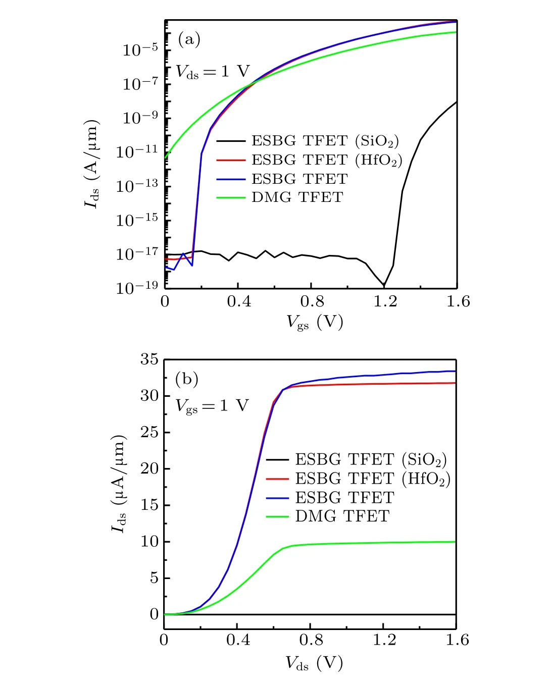
Fig. 2. (a) Transfer characteristics and (b) output characteristics comparison for the ESBG TFET and the DMG TFET.
Figure 3(a)shows the variation in the electric field along the cutlineC1(as shown in Fig. 1). The peak electric field is lied at the corners due to the point tunneling in the device.The variation in the electric field is reflected in the energy band along the cutlineC1,as observed in Fig.4(a). It is obvious that the value of energy band range over which tunneling takes place and the value of the average tunneling width varies withLs,the higher the value of energy band range over which tunneling takes place, the lower the value of the average tunneling width,the higher the charge carrier transmission probability,and henceIonis enhanced. Moreover,it is obvious from Fig.3(b)that the peak electric field at the source corners along the cutlineC2(as shown in Fig.1)is higher,which infers the line tunneling in the ESBG TFET.Figure 4(b)shows the variation in the energy band at the source corners along the cutlineC2. More energy band bending at the source corners along the cutlineC2will result in a higherIon. However,the differences of electric field and energy band along the cutlineC2betweenLs=15 nm andLs=25 nm are not obvious.

Fig.3. Electric field variation along the cutline(a)C1 and(b)C2 for the ESBG TFET with different Ls.
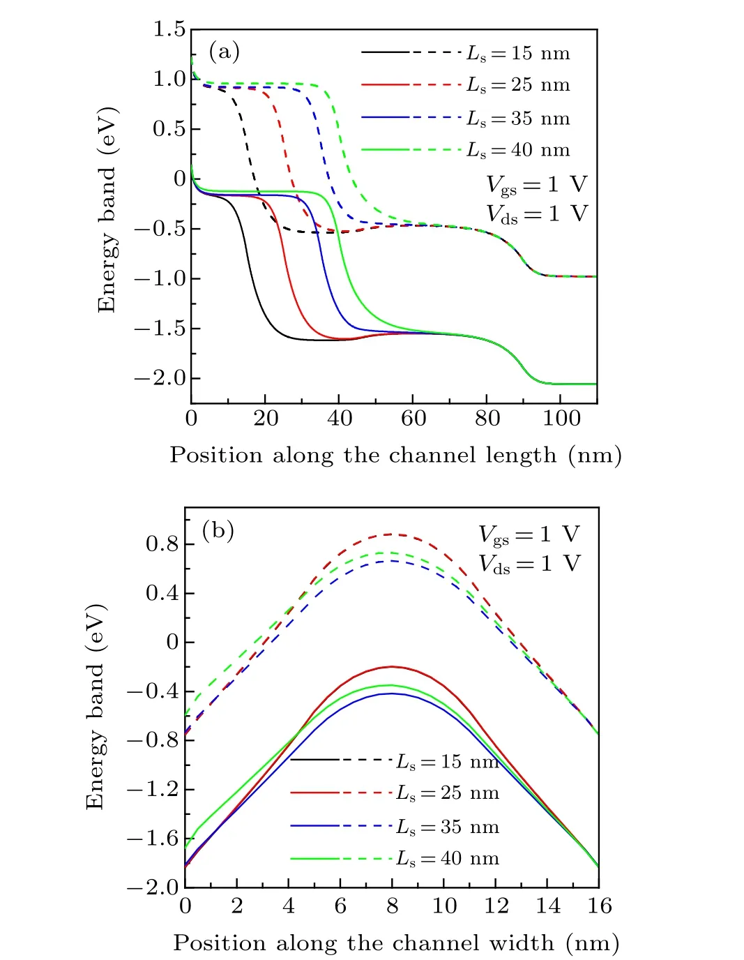
Fig.4. Energy band variation along the cutline(a)C1 and(b)C2 for the ESBG TFET with different Ls.
Figure 5(a)shows the effects ofLsonIonandIon/Iofffor the ESBG TFET. TheIonincreases with increase inLswhen the value ofLsis lower than 35 nm, butIondegrades afterLsof 35 nm. Moreover, theIon/Ioffdegrades rapidly whenLsis larger than 15 nm due to the increase inIoff. Therefore, in terms of enhancedIonandIon/Ioff,the optimum value ofLsis set to 25 nm for the ESBG TFET.Figure 5(b)shows the output characteristics for the ESBG TFET with four values ofLs.The ESBG TFET withLsof 35 nm exhibits improved drain current in comparison with other threeLsvalues.
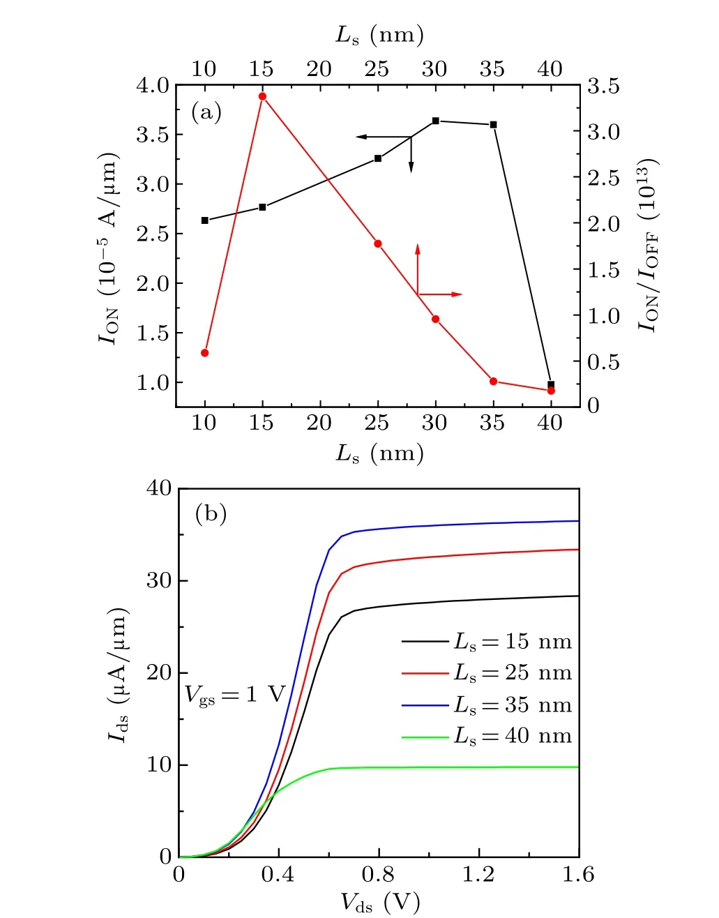
Fig.5.(a)Ion,Ion/Ioff and(b)output characteristics for the ESBG TFET with different Ls.
3.2. Parasitic capacitance and radio-frequency performance for the ESBG TFET
Parasitic capacitances impact the performances of TFET significantly at high frequency since they establish a feedback path between output and input, which leads to parasitic oscillations as well as signal distortion. These parasitic capacitances contain gate-to-source capacitanceCgs, gate-to-drain capacitanceCgd. The dependences ofCgs,Cgd, and transconductance(gm)onVgsfor the ESBG TFET with differentLsare illustrated in Fig. 6. It is obvious that for the ESBG TFET withLs= 15 nm,Cgsis lower thanCgdwhenVgsis larger than 0.3 V.Cgdincreases rapidly due to the fact that a large number of electrons are accumulated in the channel at the gate interface,whileCgsremains almost unaffected with rise inVgs.The gate capacitanceCggis the sum ofCgsandCgd. Therefore,the main component of the gate capacitanceCggisCgd. However, because of the increase of the overlap between the gate and the source regions for the ESBG TFET withLs=35 nm,Cgsis larger thanCgdwhenVgsis less than 1.3 V. Therefore,Cggis mainly determined byCgsfor most of theVgsrange at largerLs. However,Cgdis also the main component ofCggwhenVgsis larger than 1.3 V, which is due to the fact that the increase of the electron concentration in the channel leads toCgdincreasing rapidly withVgs. However, the values ofCgsandCgdare very large for the ESBG TFET withLs=40 nm whenVgsis larger than 1.3 V, which will deteriorate the high-frequency characteristics of TFET.Also,gmis an important parameter for analogue applications of the TFET which converts the gate-source voltage into the drain-source current. It is obvious from Fig. 6(c) thatgmfor the ESBG TFET withLs=35 nm is larger than that of the ESBG TFET withLs=15 nm, 25 nm and 40 nm. The higher thegmof the ESBG TFET, the better the sensitivity for the conversion of gate-source voltage into drain-source current,the better the linearity and high-frequency characteristics.
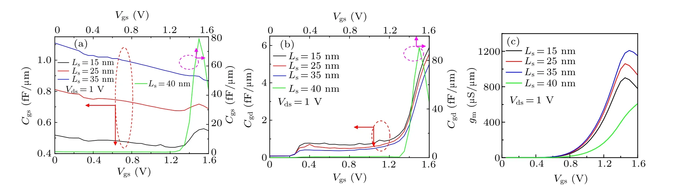
Fig.6. (a)Cgs,(b)Cgd,and gm for the ESBG TFET with different Ls.

The performance parameters of the ESBG TFET aboutIon/Ioff,gm,fTand GBP as compared with those of the recently reported TFET structures are given in Table 2. The proposed structure provides higherIon/Ioff,and largergmthan those of other reported TFET structures. Moreover,the ESBG TFET offers two times improvement infTand four times increase in GBP as compared to the recently reported ESDG TFET.
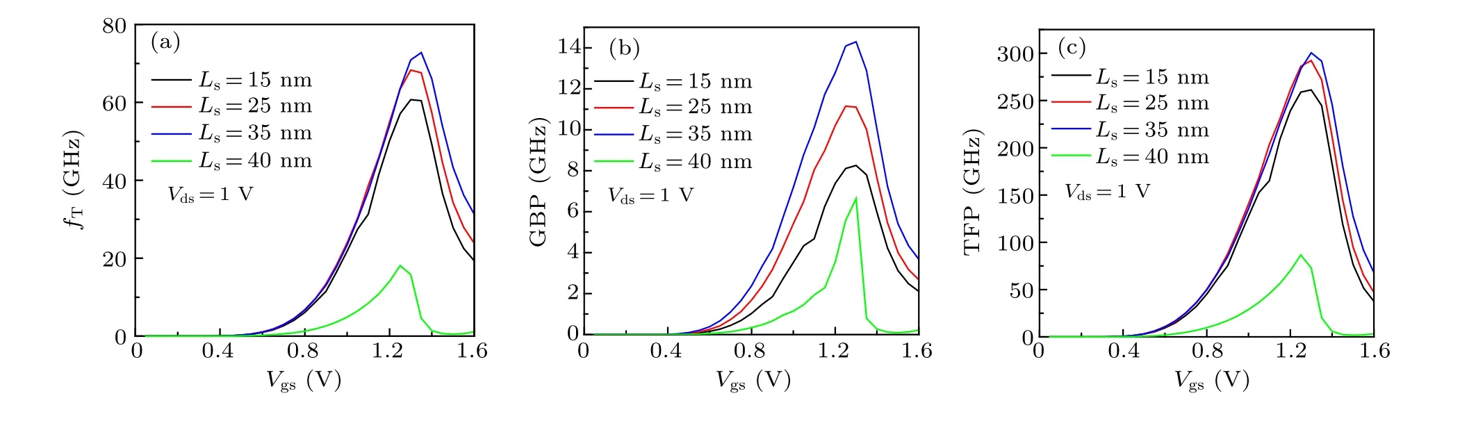
Fig.7. Characteristics of(a) fT,(b)GBP,and TFP for the ESBG TFET with different Ls.

Table 2. Comparison of performance parameters of the ESBG TFET with the recently reported TFETs.
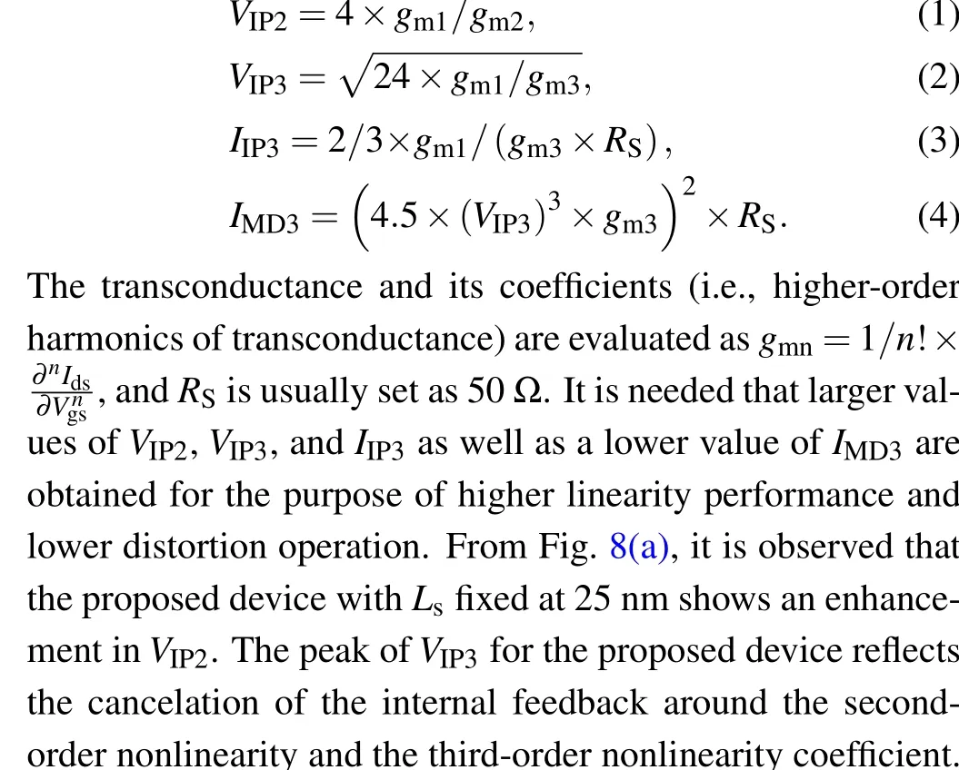
The variation of the second and third-order voltage intercept points(VIP2,VIP3),the third-order input interception point(IIP3), and the third-order intermodulation distortion (IMD3)withVgsfor the proposed device with differentLsare analyzed.The equations of these parameters can be written as follows:
The second- and third-order harmonic distortions(HD2,HD3)are analyzed in order to understand the distortion characteristics of the device,and the equations about HD2and HD3can be written as
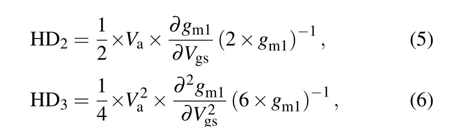

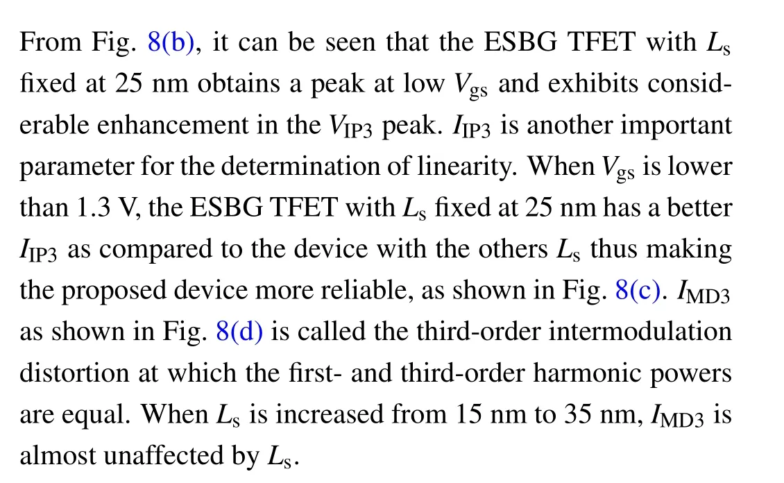
Fig.8. (a)VIP2,(b)VIP3,(c)IIP3,and(d)IMD3 for the ESBG TFET with different Ls.

Fig.9. (a)HD2 and(b)HD3 for the ESBG TFET with different Ls.
whereVais the amplitude of the input signal, which is fixed at 50 mV.It is obvious that the proposed device withLsfixed at 15 nm provides less HD2and HD3than the device with the other length ofLs. Therefore,the noise in the proposed device withLsfixed at 15 nm will be less. Consequently, it can be concluded that the proposed device withLsfixed at 15 nm is more linear with higher reliability.
4. Conclusions
The dc characteristics,analog/rf parameters and linearity parameters for ESBG TFET are analyzed. The results shows that the ESBG TFET can achieve significant improvement in parameters likeIon/Ioff,gm,fT, GBP,and TFP.The length of the source region for ESBG TFET is optimized to increase the point and line tunneling at the tunneling junction. It can be concluded that the optimum value ofLsis set to 25 nm in terms of enhancedIonandIon/Ioffof 1013. However, the parameters such asgm,fT,GBP,and TFP are slightly enhanced whenLsis set to 35 nm. Moreover, the ESBG TFET offers two times improvement infTand four times increase in GBP as compared to the recently reported ESDG TFET, thus the ESBG TFET shows better analog/rf characteristics. Furthermore,the linearity distortion parameters in terms ofVIP2,VIP3,IIP3,IMD3, HD2, and HD3for the ESBG TFET with differentLsare analyzed in order to address the nonlinearity issue.
猜你喜欢
设计(2022年8期)2022-05-25
艺术品鉴(2021年30期)2021-11-26
上海故事(2019年5期)2019-05-21
校园英语·上旬(2018年10期)2018-10-25
新青年(2018年3期)2018-03-16
青春期健康(2017年14期)2017-03-24
喜剧世界(2016年9期)2016-11-26
恋爱婚姻家庭(2015年28期)2015-12-01
微型小说选刊(2015年30期)2015-11-17
恋爱婚姻家庭(2015年10期)2015-09-10
- Chinese Physics B的其它文章
- Projective representation of D6 group in twisted bilayer graphene*
- Bilayer twisting as a mean to isolate connected flat bands in a kagome lattice through Wigner crystallization*
- Magnon bands in twisted bilayer honeycomb quantum magnets*
- Faraday rotations,ellipticity,and circular dichroism in magneto-optical spectrum of moir´e superlattices*
- Nonlocal advantage of quantum coherence and entanglement of two spins under intrinsic decoherence*
- Universal quantum control based on parametric modulation in superconducting circuits*