
Spin orbit torques in Pt-based heterostructures with van der Waals interface∗
2021-09-28 02:17QianChen陈倩WeimingLv吕伟明ShangkunLi李尚坤WenxingLv吕文星JialinCai蔡佳林YonghuiZhu朱永慧JiachenWang王佳晨RongxinLi李荣鑫BaoshunZhang张宝顺andZhongmingZeng曾中明
Chinese Physics B 2021年9期
关键词:文星
Qian Chen(陈倩)Weiming Lv(吕伟明)Shangkun Li(李尚坤)Wenxing Lv(吕文星)Jialin Cai(蔡佳林)Yonghui Zhu(朱永慧)Jiachen Wang(王佳晨)Rongxin Li(李荣鑫)Baoshun Zhang(张宝顺)and Zhongming Zeng(曾中明)
1Key Laboratory of Multifunctional Nanomaterials and Smart Systems,Suzhou Institute of Nano-Tech and Nano-Bionics,Chinese Academy of Sciences,Suzhou 215123,China
2Nanchang Nano-Devices and Technologies Division,Suzhou Institute of Nano-Tech and Nano-Bionics,Chinese Academy of Sciences,Nanchang 330200,China
3Physics Laboratory,Industrial Training Center,Shenzhen Polytechnic,Shenzhen 518055,China
Keywords:spin orbit torque,MoTe2,van der Waals interface,crystal symmetry
1.Introduction
The current-induced manipulation of magnetization realized by spin–orbit torques(SOTs)in ferromagnet/heavy-metal(FM/HM)heterostructures is one of the most active research areas in spintronics.[1,2]SOT arising from the transfer of orbital angular momentum from the lattice to the spin system,is determined by the spin–orbit coupling(SOC)in the HM and at the interface of FM/HM.Due to the limited SOT efficiency and the two-fold rotational symmetry of traditional HM such as Pt,a deterministic and energy-efficient magnetization switching in a system with perpendicular magnetic anisotropy(PMA)is not allowed without an external magnetic field,which greatly limits the application of SOT in low-energy integrated spintronic devices.[3]
Interface engineering of FM/HM gives new opportunities to modulate the SOT effect,which has been confirmed by lots of pioneering works.Qiuet al.reported that the large spin absorption at the Ru interface can be employed to manipulate the SOTs in HM/FM/Ru multilayers.[4]Razaviet al.modified the conventional SOT heterostructure by inserting a wedged lightmetal layer at the HM/FM interface,and achieved the fieldfree magnetization switching in a PMA system.[5]Recently,based on the strong interfacial orbital hybridization between Pt and Co,enhanced SOT efficiency and induced out-of-plane torques in Pt/Co/Py were reported by Shuet al.by inserting an ultrathin Co layer into Pt/Py.[6]However,all of these works require strict control of film thickness,which puts forward high requirements for the film-deposition techniques.Moreover,it is difficult to control the crystallinity of the metal films especially in the low thickness regime.
Extensive research efforts have been devoted to facilitate the practical use of two-dimensional(2D)van der Waals(vdW)materials in SOT devices.[7]Relying on layered structures,2D vdW materials are possible to realize smooth surfaces with atomic-scale flatness,which facilitates interface engineering of FM/HM.Moreover,high-quality multilayer structures can be easily achieved by stacking 2D vdW interfaces together with metal films because of the absence of dangling bonds on the surface.[8]Integrating 2D vdW materials in SOT devices has shown many advantages,the most striking of which is the out-of-plane damping-like SOT induced by the low crystal symmetry of 2D vdW materials such as WTe2[9,10]and MoTe2.[11]This novel observation holds a great promise for field-free switching of the perpendicularly magnetized system.In addition,similar to the effects of spin absorption observed in metal films,Debashis et al.reported that the spin Hall efficiency of the ultra-thin Ta can be enhanced by more than 25 times when a monolayer(ML)WSe2is inserted as an underlayer of Ta/Co60Fe20B20due to spin absorption effect at the interface.[12]Xie et al.demonstrated that the SOT efficiency in Pt/[Co/Ni]2can be greatly enhanced by introducing a MoS2underlayer,which is caused by the orbital hybridization at the interface of Pt/Co due to MoS2.[13]However,it is still lack of evidence whether the low crystal symmetry of 2D vdW materials can be used in interface engineering of conventional FM/HM heterostructures.Recent studies have shown that the low-symmetry MoTe2has both a large SOT efficiency and a long spin diffusion length at room temperature,making it an excellent candidate for simultaneous spin generation,transport and detection.[14]
In this paper,the SOT effect based on a multilayer structure consisted of Pt/MoTe2/Ni is investigated,in which the monolayer 1T′-MoTe2with low crystal symmetry is used as the insert layer to engineer the interface between Pt and Ni.Although retains bulk inversion symmetry,the 1T′-MoTe2provides a unique opportunity to study the symmetries and interface relevant spin–orbit torques,because its surface symmetry is limited to just one mirror plane.The SOT efficiency is improved which is rationalized by interfacial engineering effects such as orbital hybridization and the increased interfacial scattering.In addition,an out-of-plane damping-like torque is observed when the current is applied perpendicular to the mirror plane of MoTe2.We attribute this special torque to the symmetry breaking of the system caused by monolayer MoTe2.
2.Materials and methods
To prepare the samples,2 nm Ti and 4 nm Pt films are deposited onto high resistivity Si/SiO2wafers by electron beam evaporation(EBE).Pt is employed as a spin source where charge-to-spin conversion is happened due to the spin Hall effect(SHE),and the fresh Pt surface is used to assist the exfoliation of monolayer MoTe2,because the MoTe2/Pt binding is stronger than the corresponding interlayer binding in MoTe2.[15]After the exfoliation,Si/SiO2/Ti/Pt/MoTe2is reinstate to the high vacuum chamber in rapid sequence to avoid excessive interface degradation or oxidation,and provide a relatively clean interface for the subsequent Ni(6 nm)deposition by EBE.During the deposition,the base pressure is maintained at about 5×10⁻⁶torr.The deposition rate of Ni is well controlled as low as 0.1˚A/s,and the whole process is carried out with a room-temperature water-cooled system.Therefore,the energy of Ni atoms acting on MoTe2is low enough to avoid damaging the vdW monolayer.Figure 1(a)displays an optical image of the Pt/MoTe2/Ni heterostructure.Monolayer MoTe2can be resolved by the optical contrast,which is corroborated by direct topography measurements with an atomic force microscope(AFM),and the 0.8 nm step in the height profile shown in the inset of Fig.1(a)exactly matches the MoTe2monolayer thickness.We perform cross-sectional transmission electron microscopy(TEM)imaging on a Pt/MoTe2/Ni device(Fig.1(b))as initially identified by AFM.The delamination of Ni and Pt films is clearly seen,however,monolayer MoTe2is hardly to be observed because of the limited resolution.Crystal structure of the films is elucidated using x-ray diffraction(XRD).The corresponding XRD patterns of the films are displayed in Fig.1(d),where crystalline peaks of MoTe2(002)and(004),Pt(111)and Ni(111)are detected,indicating that the crystal surface of MoTe2is normal to the c-axis with the plate-shaped surface parallel to the ab plane.To investigate the crystal quality of the exfoliated MoTe2,Raman spectroscopy with a 532 nm excitation laser is utilized.Characteristic Raman peaks are observed:Agmodes at about 128 cm−1,163 cm−1and 265 cm−1,Bgmode at about 189 cm−1(Fig.1(e)),which are in accordance with the Raman shifts predicted from theoretical calculations.[16]Polarized Raman spectroscopy is carried out to confirm the orientation of the crystal axes of MoTe2.The polar plot of the angle dependent intensities of the Agmode with the frequency~265 cm−1is shown in Fig.1(f),which is in good agreement with previous studies[17]and proves that the longitudinal axis of the exfoliated MoTe2is along its a-axis(typically perpendicular to the mirror plane of MoTe2,as marked in Fig.1(c)).
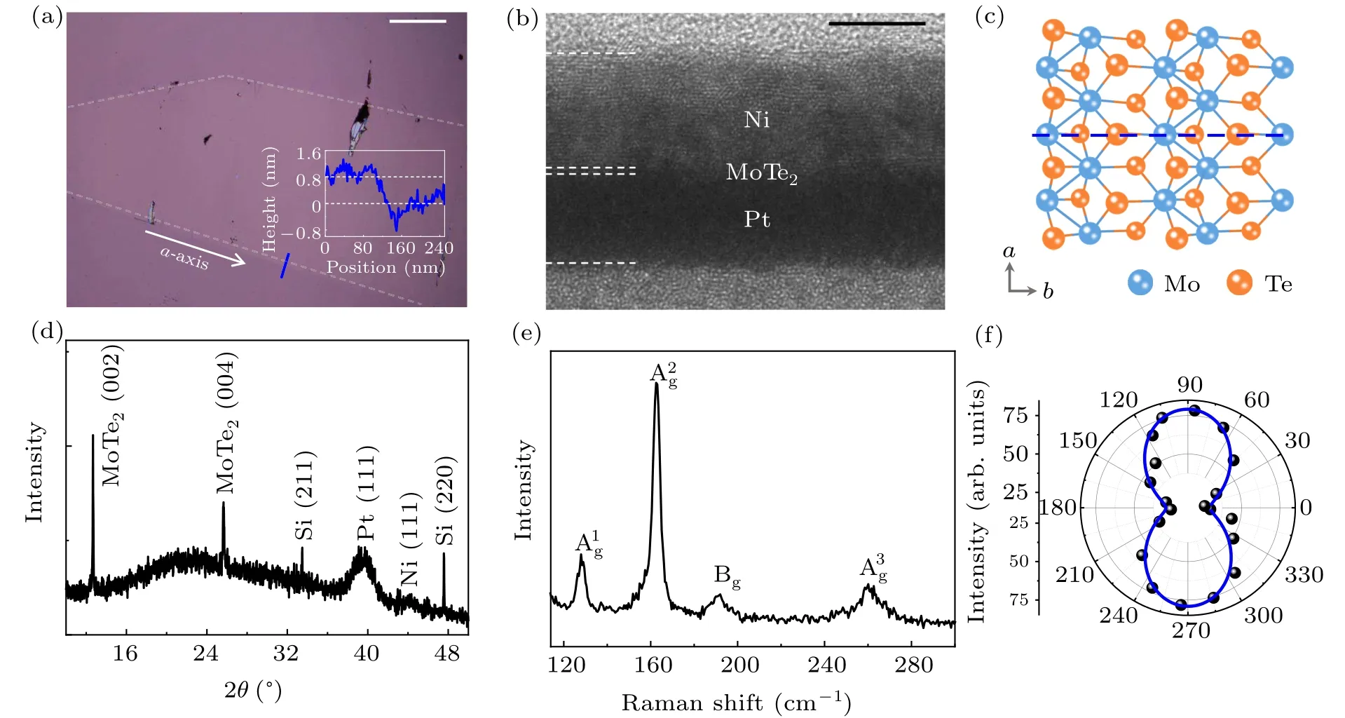
Fig.1.(a)Optical microscopy image of a Pt/MoTe2/Ni sample.The scale bar is 20µm.The line profile drawn across the terrace indicates a step height of~8˚A.(b)Cross-sectional TEM images of Pt/MoTe2/Ni multilayer structure.The scale bar is 5 nm.(c)Structure of the 1T′-MoTe2 crystal depicted in the ab plane,where the mirror plane is depicted by the dashed blue line.(d)XRD patterns of Pt/MoTe2/Ni.(e)Raman spectra of the exfoliated MoTe2.(f)The polar plots of the angle dependent intensities of Ag mode with the frequency~265 cm−1.The angle is zero when the excitation laser polarization is parallel to the longitudinal axis of the exfoliated MoTe2.
3.Results and discussion
To fabricate Pt/MoTe2/Ni devices for the SOT study,the samples are patterned into micro-strips by electron-beam lithography and Ar ion etching,and electrical connections are made by Ti/Au contact pads.The long axis of the micro-strip is along the a-axis of MoTe2,so that the current is applied along the low-symmetry crystal axis of MoTe2,leading to the breaking of inversion symmetry at the interface.Pt/Ni device is also fabricated for comparison.Using the circuit shown in Fig.2(a),we measure the spin orbit torques by the technique of spin-torque ferromagnetic resonance(ST-FMR).[18]During the measurement,an alternating current I with a fixed frequency f is applied through the device,and a sweeping magnetic field H is applied in the film plane,with the angleφ between H and the long axis of the micro-strip kept at 45°unless otherwise indicating.The output power of the microwave signal generator is 18 dBm.All the measurements are performed at room temperature.In ST-FMR,the torques generated by the current excite the magnetic moment away from equilibrium and cause it to precess,creating a time-dependent change in the resistance of the device due to the anisotropic magnetoresistance(AMR)in Ni.The mixing between the applied alternating current and the oscillating resistance further generates a mixing voltage Vmixdue to the spin torque diode effect as given by[18,19]
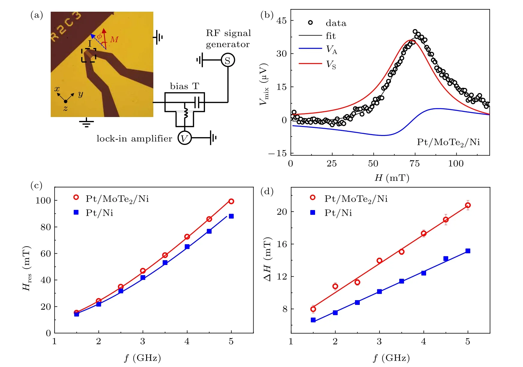
Fig.2.(a)Optical images of the device including contact pads,with the circuit used for ST-FMR measurement.(b)Measured ST-FMR spectra for Pt/MoTe2/Ni,with the magnetization oriented at 45° relative to the current direction and f=4 GHz.The lines are fits to Eq.(1)showing the symmetric VS and antisymmetric VA resonance components.(c)Frequency dependence of the resonance field for Pt/Ni and Pt/MoTe2/Ni devices.The solid lines represent the theoretical fitting using the Kittle equation.(d)The linewidthΔH extracted from the fitting of the ST-FMR signal as a function of the resonant frequency f.The solid lines are the linear fittings.
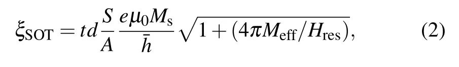
whereµ,e,t,d,Ms,and Meffare the magnetic permeability in free space,electronic charge,thickness of ferromagnetic layer,thickness of nonmagnetic layer,saturation magnetization and effective magnetization of Ni,respectively.
Frequency dependences of HresandΔH are illustrated in Figs.2(c)and 2(d),respectively,where we find that both the resonance field and linewidth of Ni are increased after the insertion of monolayer MoTe2especially at high frequencies,implying the regulation of Ni magnetism by MoTe2.The effective magnetization Meffis extracted by fitting the f versus Hresdata to the Kittel equation(as shown in Fig.2(c)),f=(γ/2π)[(Hres+Hk)(Hres+Hk+4πMeff)]1/2.[20]Here,Hkdenotes the in-plane magnetic anisotropy which is close to zero,and Meffincorporates the Msand the surface anisotropy field Hs,that is 4πMeff=4πMs−Hs.[21]Hs>0 is defined as surface anisotropy in the film normal and Hs<0 stands for the surface anisotropy in the film plane.The extracted 4πMeffof Pt/MoTe2/Ni is 232.43±4.40 mT,smaller than the value extracted from Pt/Ni(286.39±7.94 mT).The reduction of Meffin Pt/MoTe2/Ni indicates either a decrease of Msor an increased PMA in Ni induced by MoTe2.Previous work has shown that 2D transition-metal dichalcogenides should not result in a change in Ms,[11,22]but are likely to enhance the PMA of the magnetic layer due to the modification of the orbital hybridization.[13]Accordingly,compared with Pt/Ni bilayers,the increased PMA field in Pt/MoTe2/Ni is about 53.96 mT,which may arise from the interfacial d–d orbital hybridization of Pt,Mo and Ni.[6,13]Using the fitted values of Meff,the SOT efficiency of Pt/Ni is calculated as 0.125±0.011,close to the value reported by Bose et al.[23]but slightly higher compared to other reports[24]which can be attributed to the impurity present in Pt for different lab conditions.Comparatively,the SOT efficiency of Pt/MoTe2/Ni is extracted as 0.197±0.016,much larger than the value extracted from Pt/Ni.Such an enhancement ofξSOTmay be related to the increased spin–orbital coupling(SOC)caused by interfacial d–d orbital hybridization.[6,13]On the other hand,recently,Novakov et al.demonstrated that insertion of up to two monolayers of WSe2is able to enhance the spin transfer torques in a Rashba system by up to 3 times,[25]indicating that low layer count 2D vdW materials can be used as an interfacial scattering promoter in heterostructure interfaces without quenching the original polarization.Although there is absent of direct evidences whether MoTe2fits the Rashba system or not,[26]the increased scattering will enhance the spin fluctuation at the interface as well,which amplifies the spin current transmission between Pt and Ni and then improve the SOT efficiency in Pt/MoTe2/Ni device.[27,28]
Figure 2(d)shows the linear relationships betweenΔH and f,which are well fitted with the equationΔH=ΔH0+2πfα/γ,[29]whereαis the Gilbert damping of Ni.The linewidth contribution from inhomogeneity can be estimated from the value ofΔH0.Here,similar values ofΔH0(~25 Oe)for Pt/Ni and Pt/MoTe2/Ni are extracted,suggesting that the insert of MoTe2does not cause significant inhomogeneity in Ni.Fitting results are listed in Table 1.Gilbert damping of Pt/Ni device is 0.0695±0.0018,and increases to 0.0999±0.0050 after inserting monolayer MoTe2.The increased damping indicates the additional loss of the spin angular momentum dissipated in Ni.According to the spin pumping theory raised by Tserkovnyak et al.,[30,31]a moving magnetization vector causes pumping of spins into adjacent nonmagnetic layers.This spin transfer affects the magnetization dynamics similar to the Landau–Lifshitz–Gilbert phenomenology,and an additional Gilbert damping is induced when the nonmagnetic layers efficiently relax the injected spins.Here,in Pt/MoTe2/Ni,spin currents generated from Ni are relaxed in Pt,and the MoTe2may act as a scattering promoter,increasing the spin transport efficiency at the interface which is similar to the model provided by Novakov et al.[25]and Lee et al.[27,28]However,further studies regarding to the spin pumping effect in systems with 2D vdW interfaces are still needed.
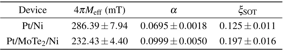
Table 1.The 4πMeff,αandξSOT extracted from ST-FMR measurements.
To determine the effect of interfacial symmetry breaking induced by MoTe2,we analyze the extracted fit parameters VSand VAas functions of the applied field angle.Representative data for Pt/MoTe2/Ni and Pt/Ni are shown in Figs.3(a)–3(d).Because of the high-symmetry of Pt,the generated spin orbit torques by Pt are consist of an out-of-plane fieldlike torque,τA∝ˆm׈y,and an in-plane damping-like torque,τS∝ˆm×(ˆm׈y),so that VAand VSconform to the angle dependency of sin(2φ)cos(φ).[32]Note that we define the applied current as always being in theˆx direction(Fig.2(a)).Recent studies have demonstrated that,apart fromτAandτS,an out-of-plane damping-like torqueτBis also allowed when the system has a single mirror symmetry and the current is applied perpendicular to this mirror plane,[9–11]as is the case for our Pt/MoTe2/Ni device.To extractτB,we fit the angular dependence of VAby the simple addition of a termΔVA(Fig.3(b))proportional to sin(2φ),[9]

where the fit parameter B representsτB∝ˆm×(ˆm׈z).The ratio B/A=0.104±0.037,which is about three-times smaller than the value obtained in the monolayer MoTe2/Py structure reported by Stiehl et al.[11]This is reasonable since both Pt and MoTe2contribute toτAandτSin Pt/MoTe2/Ni device.
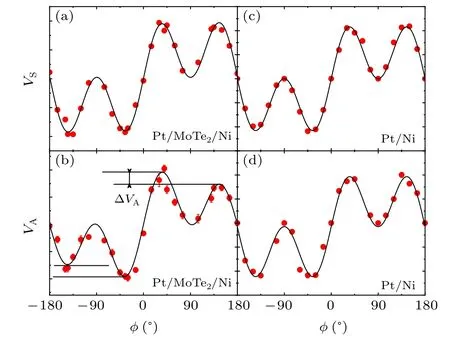
Fig.3.Dependence on the applied field angle for the(a)symmetric,VS,and(b)antisymmetric,VA,components of mixing voltage for Pt/MoTe2/Ni,with current applied parallel to the a-axis of MoTe2.(c)VS and(d)VA of mixing voltage for Pt/Ni.The frequency of the microwave during measurement is 4 GHz.
To further demonstrate the symmetry dependence ofτB,Pt/MoTe2/Ni device with current applied parallel to the b-axis of MoTe2is studied.Figure 4 shows the antisymmetric STFMR component VAas a function ofφ,where we find no evidence ofΔVAsinceτBis forbidden by symmetry in this case.[11]
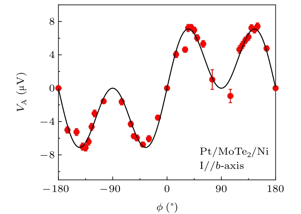
Fig.4.Antisymmetric ST-FMR component VA for Pt/MoTe2/Ni as a function of in-plane magnetic-field angle,with current applied parallel to the b-axis of MoTe2.The microwave frequency is 4 GHz.
4.Conclusions
In summary,we have demonstrated that it is feasible to engineer the interface of conventional Pt based FM/HM heterostructures by inserting monolayer 2D MoTe2with low crystal symmetry.The out-of-plane magnetic anisotropy of Ni is increased due to the interfacial d–d orbital hybridization of Pt,Mo and Ni.The Gilbert damping of Ni is enhanced from 0.0695 in Pt/Ni to 0.0999 in Pt/MoTe2/Ni due to the additional loss of the spin angular momentum caused by MoTe2.The SOT efficiency of Pt/MoTe2/Ni is up to 0.197,much larger than that of Pt/Ni.We suspect that the improved SOT efficiency is related to the interfacial orbital hybridization and the enhanced interfacial scattering of spin current induced by monolayer MoTe2.Particularly,an out-of-plane damping-like torque is induced and shows dependence on the interfacial inversion symmetry of the system.When the current is applied along the low-symmetry crystal axis of MoTe2,the out-ofplane damping-like torque is observed,and when the current is applied parallel to the mirror plane,it is invisible.Our results suggest a strategy for achieving efficient manipulation of magnetic devices with PMA.To date,various approaches for field-free SOT-induced magnetization switching of PMA structures have been proposed and demonstrated,for example,switching using a wadge oxide capping layer,[33]a polarized ferroelectric substrate,[34]lateral SOT,[35]introducing an interlayer coupling or an exchange bias field.[36,37]Compared with these previous methods,2D vdW interface induced outof-plane SOT broadens the scope of material engineering for conventional Pt-based SOT devices,and the efficiency of SOT is improved coupled with the additional symmetry breaking,making it a promising candidate for magnetic memory and logic devices driven by SOT.
猜你喜欢
安徽农业科学(2022年9期)2022-05-17
现代职业教育·高职高专(2022年16期)2022-05-05
土壤学报(2022年1期)2022-03-08
北方音乐(2020年23期)2020-12-24
意林·作文素材(2017年18期)2017-10-19
杂文选刊(2017年9期)2017-09-06
恋爱婚姻家庭(2017年28期)2017-09-01
校园英语·上旬(2017年7期)2017-07-13
中学科技(2017年4期)2017-04-22
中学科技(2017年3期)2017-04-10
- Chinese Physics B的其它文章
- Multiple solutions and hysteresis in the flows driven by surface with antisymmetric velocity profile∗
- Magnetization relaxation of uniaxial anisotropic ferromagnetic particles with linear reaction dynamics driven by DC/AC magnetic field∗
- Influences of spin–orbit interaction on quantum speed limit and entanglement of spin qubits in coupled quantum dots
- Quantum multicast schemes of different quantum states via non-maximally entangled channels with multiparty involvement∗
- Magnetic and electronic properties of two-dimensional metal-organic frameworks TM3(C2NH)12*
- Preparation of a two-state mixture of ultracold fermionic atoms with balanced population subject to the unstable magnetic field∗