
Atomic and electronic structures of p-type dopants in 4H-SiC
2021-09-28 02:18LingyanLu卢玲燕HanZhang张涵XiaoweiWu吴晓维JingShi石晶andYiYangSun孙宜阳
Chinese Physics B 2021年9期
Lingyan Lu(卢玲燕),Han Zhang(张涵),Xiaowei Wu(吴晓维),Jing Shi(石晶),and Yi-Yang Sun(孙宜阳),§
1Department of Physics,Jiangxi Normal University,Nanchang 330022,China
2State Key Laboratory of High Performance Ceramics and Superfine Microstructure,Shanghai Institute of Ceramics,Chinese Academy of Sciences,Shanghai 201899,China
Keywords:wide band gap semiconductors,p-type doping,SiC,density functional theory
1.Introduction
Power electronic devices have found more and more applications in our everyday life,including fast-chargers for mobile electronic devices,inverters for electricity generation by solar and wind energy,electric cars and trains,just to name a few.Silicon-based devices are becoming more and more mature.Meanwhile,they are also approaching the limits of device specifications,in particular,breakdown voltage.To meet the market demands on high working voltage,as well as on device miniaturization,wide-band-gap semiconductors have been proposed for power electronics.[1]Generally,the breakdown voltage is proportional to the band gap.[2]Even though many wide-band-gap semiconductors have been explored,silicon carbide(SiC)and gallium nitride(GaN)are currently the two most successful materials.A key barrier for discovering new power electronic materials is bipolar doping for making p–n junctions.By far,SiC and GaN are the only two materials that can be sufficiently doped to both n-and p-types among semiconductors with the band gap greater than 3 eV.[3,4]Except for rare cases,such as diamond,p-type doping is usually more difficult than n-type doping.[5]
SiC and GaN have large band gaps of 3.27 eV and 3.50 eV,respectively.[6,7]As a result,both of them exhibit a high breakdown field of 3–4 MV/cm,[8,9]an order of magnitude higher than that of silicon.In comparison,SiC has a thermal conductivity of about 4.7 W·cm−1·K−1at room temperature,significantly higher than that of GaN[10,11]and therefore,is more favored for high-power and high-temperature applications.On the other hand,GaN exhibits high electron mobility of 2000 cm2·V−1·s−1,significantly higher than that of SiC.[12,13]The values quoted above are for 4H-SiC,which is one of the numerous polymorphs of SiC and most favored for power electronic devices by overall consideration on electron mobility,breakdown field,thermodynamic stability,etc.[14]
Trivalent elements(B,Al and Ga)are the choice of p-type dopants for SiC.Currently,Al is the most commonly adopted in making power electronic devices.However,Al in SiC is not a sufficiently shallow acceptor.Its acceptor level is experimentally reported to be 0.22 eV or greater,[15]rendering the p-type doping still an issue in device fabrication.A number of theoretical studies reported atomic and electronic structures of ptype dopants in different polymorphs of SiC.[16–19]However,a key structural feature,namely,off-center displacement of the dopant atom,has been missed until recently a hybrid density functional was adopted in the calculation.[20]Such distortion by breaking the local C3vsymmetry to a C1h(or Cs)pointgroup symmetry has been noticed in an earlier work.[21]Such distortions are also known for other wide-band-gap semiconductors,such as ZnO and GaN.[22]
In this paper,we study the atomic and electronic structures of group-III elements(B,Al and Ga)in 4H-SiC based on hybrid density functional calculations.We consider the possibility of dopants on Si and C sites and for both cases we consider the wurtzite-like(wz)and zincblende-like(zb)sites.We also study the possible off-center distortions and determine the stable and metastable structures for these p-type dopants.Employing chemical potentials for all elements in our defect formation calculations,we study the effect of secondary phases on the doping.We compare the acceptor levels of the group-III elements in 4H-SiC at all possible local structures,which determine the doping efficiency and may provide a useful guide in the future dopant engineering in 4H-SiC.
2.Computational method
Our calculations were based on density functional theory(DFT)implemented in Vienna ab initio simulation(VASP)package,[23]which describes the interaction between the ioncores and valence electrons by projector augmented wave(PAW)potentials.[24]Plane waves with cutoff energy of 30 Ry were taken as the basis set.We used the hybrid exchange-correlation functional of Heyd,Scuseria and Ernzerhof(HSE),[25]which includes 25%of Hartree–Fock exchange energy with its long-range part removed by using the error function.The supercell method was used to model the defects.A 4×4×1(128-atom)supercell and a 5×5×2(400-atom)supercell were used in our calculations.TheΓpoint was used to represent the Brillouin zone of the defect supercells.All calculations on neutral defects,which exhibit a spin magnetic moment of 1µB,were spin-polarized.The atomic structures were fully relaxed until the calculated forces on all atoms were less than 0.5 mRy/Bohr.When optimizing the lattice constants,we used a cutoff energy of 45 Ry and a 5×5×2 Monkhorst–Pack k-point grid,which yielded a=3.071˚A and c=10.043˚A.
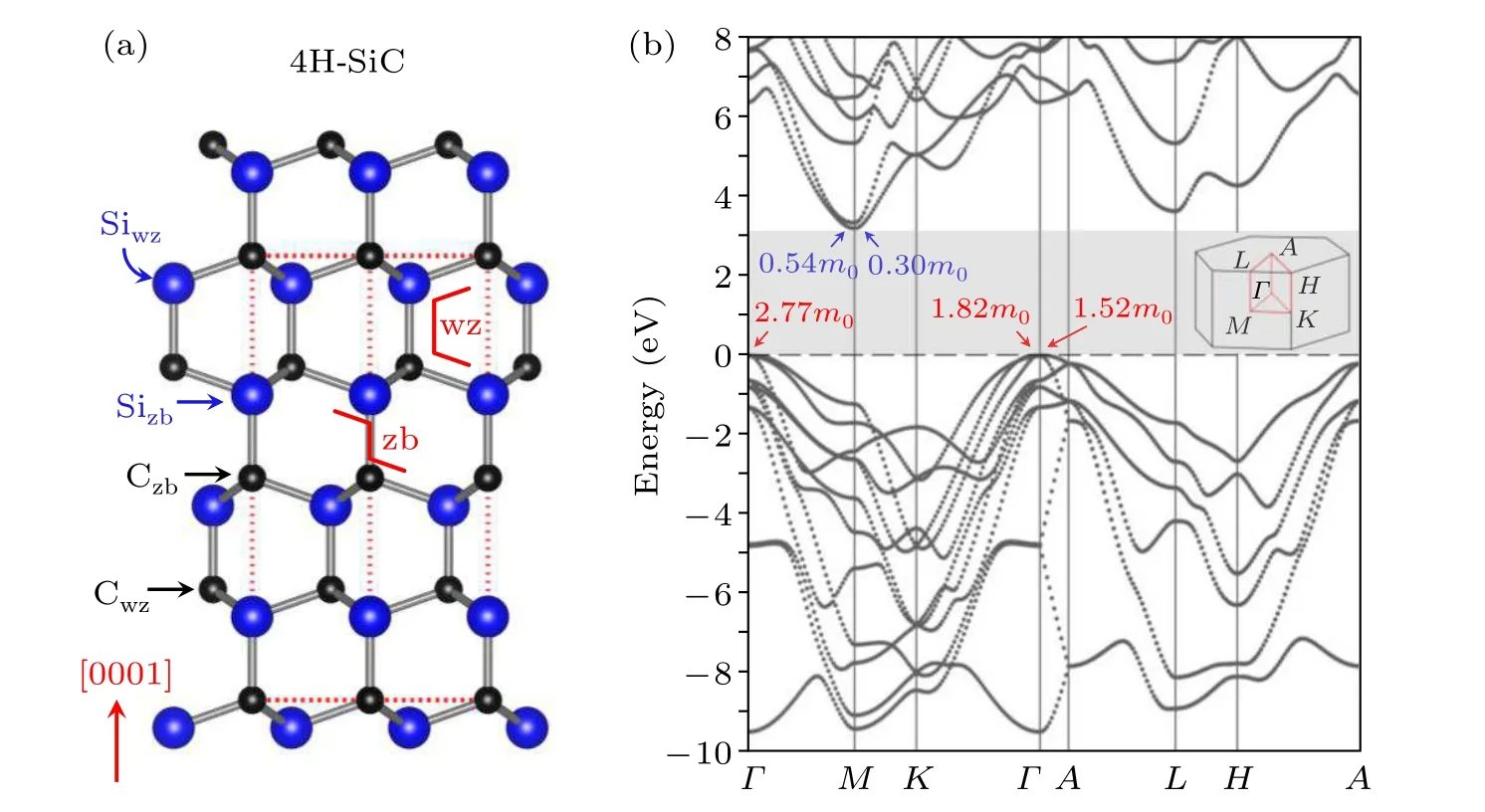
Fig.1.(a)Atomic structure of 4H-SiC from a side view.The red dashed frame marks the unit cell,which contains four Si layers and four C layers along the[0001]direction.The two red solid lines guide the eye to identify the wurtzite(wz)and zincblende(zb)local coordination for two different Si sites,referred to as Siwz and Sizb,respectively,The C sites are labeled similarly as Cwz and Czb,respectively.(b)Band structure of 4H-SiC calculated using the HSE functional.The gray region is the band gap.The electron effective masses along three directions and the hole effective masses along two directions are shown in the inset.The first Brillouin zone and the high-symmetry k-points are also shown in the inset.
3.Results and discussion
Figure 1(a)shows the atomic structure of 4H-SiC from a side view.Each unit cell contains four Si layers and four C layers along the[0001]direction.Aided by the two redcolor guiding lines,it can be seen that two of the Si layers have their local coordination environment similar to that in the wurtzite structure and another two similar to that in the zincblende structure.The two different sites are referred to as Siwzand Sizb,respectively,in this paper.The C sites are labelled similarly as Cwzand Czb,respectively.
Figure 1(b)shows the calculated band structure of 4HSiC using the HSE functional.The valence band maximum(VBM)is located at theΓpoint and the conduction band minimum(CBM)is located at the M point.The band gap is calculated to be 3.17 eV,in reasonable agreement with the experimental value.[6]The calculated electron effective masses along the M–Γand M–K directions are 0.54m0and 0.30m0,respectively,which are comparable with the measured values of 0.42m0and 0.29m0[26,27]In comparison,the hole effective masses of 2.77m0,1.82m0and 1.52m0along theΓ–M,Γ–K,andΓ–A directions,respectively,are significantly larger than those of electrons.
Next,we investigate the properties of p-type dopants(B,Al and Ga)in 4H-SiC.To study the atomic structures,we follow a procedure shown in Fig.2(a).First,we consider whether the dopant atoms occupy the Si or the C sites.Initiatively,B has an ionic radius close to C suggesting that it may favor the C sites,while Al and Ga may favor the Si sites due to the larger ionic radii.To quantify these arguments,the defect formation energy needs to be calculated.Second,as shown in Fig.1(a),4H-SiC exhibits two different sites for both Si and C atoms.It is necessary to study the occupation preference between the two sites.Third,it is relatively less discussed in the literature that these p-type dopants undergo significant distortion in the neutral charge state,referred to as defect-bound small polarons.[28]
Figure 2(b)shows the possible distortion directions.By taking a Si-site dopant(denoted by D)as an example,C0is the axial C atom with the C0–D bond parallel to the[0001]direction.C1,C2and C3are the three equatorial C atoms.In the figure,C2and C3are overlapped with each other.If the D atom is displaced along the C0–D bond,the local C3vpoint-group symmetry is preserved with two possible directions marked byΔ2andΔ′2in Fig.2(b).If the D atom is displaced along the C1–D bond,then the C3vsymmetry is broken and only a mirror passing C1,C0and the middle point between C2and C3is maintained,i.e.,Cs(or C1h)point-group symmetry.This type of distortions is marked byΔ1andΔ′1in Fig.2(b).The third type of distortions,marked byΔ3andΔ′3,also maintain the Cssymmetry only with the displacement direction of the D atom bisecting the C2–D–C3angle.
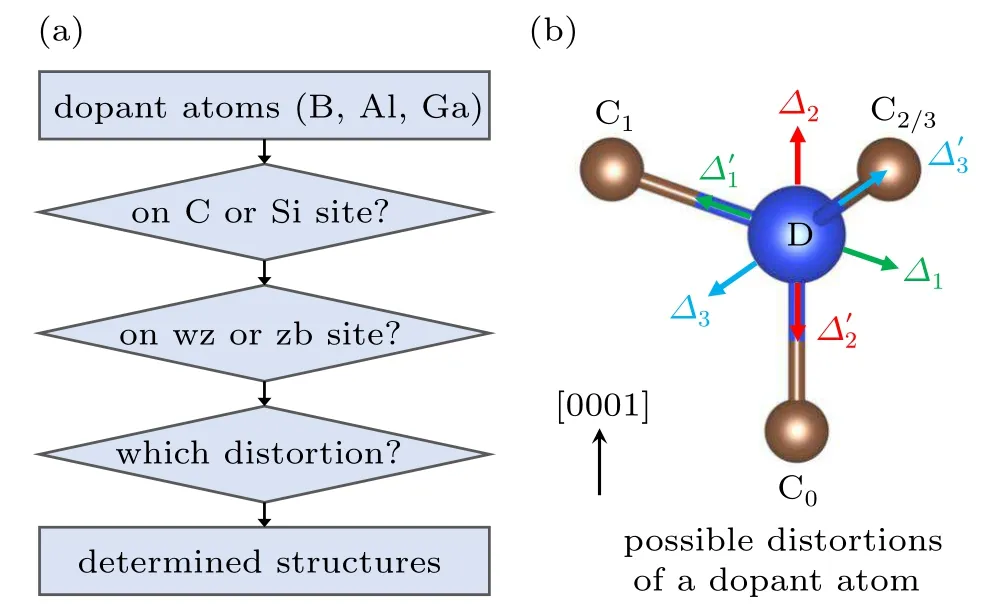
Fig.2.(a)Flow chart for determining the atomic structure of group-III dopants in 4H-SiC,including the preferences on Si or C sites and on wurtzite-like(wz)or zincblende-like(zb)sites,as well as the distortions of the dopant atoms.(b)Possible distortions of a dopant atom(denoted by D)on a Si site.C0 is the axial C atom with the C0–D bond parallel to the[0001]direction.C1,C2 and C3 are the three equatorial C atoms surrounding the Si site,where C2 and C3 are overlapped with each other.There are three possible types of displacements for the D atom.Δ1 is along the C1–D bond,Δ2 is along the C0–D bond,andΔ3 is along the direction bisecting the C2–D–C3 angle.Each of them can have an opposite direction,marked by a prime.
The defect formation energies were calculated according toΔH({µi},EF,q)=ED(q)−E0+∑ini(Ei+µi)+q(EVBM+EF),where ED(q)is the total energy of the defect supercell in charge q,E0is the total energy of the perfect supercell and{µi}are the chemical potentials.The detailed description for each term can be found in our previous work.[29]We first adopted the 128-atom supercell.To determine the allowed range for the chemical potentials{µi},it is required to satisfyµSi+µC=ΔH(4H-SiC),which is the enthalpy of formation of 4H-SiC.Also,successful doping needs to avoid the formation of secondary phases.B tends to form B4C[30]and B3Si[31]and Al tends to form Al4C3,[32]while Ga does not form stable compounds with either Si or C.For each secondary phase,the sum of{µi}with corresponding weights needs to be lower than the enthalpy of formation of that phase.The conditions to satisfy are shown in Fig.3(a)with the values of formation enthalpy for each secondary phase calculated by the HSE functional.
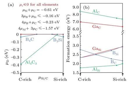
Fig.3.(a)Determination of chemical potentials for the dopant elements(µD)between C-rich(µC=0)and Si-rich(µSi=0)conditions.µB(blue line)is limited by the formation of B4C and B3Si.µAl(green line)is limited by the formation of Al4C3.µGa(red line)can be constantly 0(i.e.,Ga-rich).The conditions to satisfy are shown above the plot.All enthalpies of formation are calculated by the HSE functional.(b)Formation energy of B,Al and Ga on Si and C sites calculated by the HSE functional.For B and Al,the lines are segmented because the chemical potentials of B and Al are segmented as shown in(a).
From Fig.3(a)it can be seen thatµGacan be constantly 0(red line),meaning that the growth condition for doping Ga can be Ga-rich and there is no need to consider the formation of secondary phases.For B,due to the formation of B4C and B3Si under C-and Si-rich conditions,respectively,the growth condition for doping B cannot be overly B-rich.Nevertheless,because theΔH for the two B-induced secondary phases are small,their effect on the defect formation energy is relatively small.In comparison,the formation of Al4C3limitsµAlto be below−0.39 eV under C-rich condition,which is the favored growth condition for Al occupying Si sites.
Figure 3(b)shows that Al and Ga on C sites have high formation energies above 6 eV suggesting that it is almost impossible to have Al and Ga to occupy C sites in a significant amount.They will not be considered below.Our results show that B can occupy both Si and C sites depending on the growth condition.Under C-rich condition,B tends to occupy the Si sites,while under Si-rich condition,B tends to occupy the C sites.Even though the Al-rich condition is limited by the formation of Al4C3as mentioned above,Al on Si site still exhibits the lowest formation energy,about 1.77 eV at C-rich(or Si-poor)condition for neutral charge state.
Regarding the site preference between the wz and zb sites,our calculations show that the energy difference on the two sites is small,less than 10 meV for the two Si sites.For the two C sites,B on the Czbsite is more stable than on the Cwzsite by 16 meV.For typical growth temperature of 4H-SiC,this small energy would not result in significant occupation preference.
We next discuss the distortions.It is more convenient to discuss the stability of the distortions together with the calculated acceptor level(or ionization energy),which is obtained byε(0/−)=ED(−)−ED(0)−EVBM.Because the defects do not show different distortions in the 1−charge state,a less stable structure in the neutral charge by having a higher ED(0)will yield a lower(or shallower)acceptor levelε(0/−).Figure 4(a)shows the calculatedε(0/−)levels for B on both the Si and C sites and Al/Ga on the Si sites.For each case,we consider the occupation preference between the wz and zb sites,which ends up with eight defects.For each defect,we find three relaxed structures.
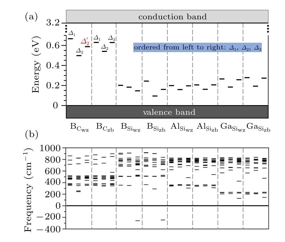
Fig.4.(a)Calculated acceptor levels(or ionization energy),ε(0/−),for B,Al,and Ga on Si and C sites using the 128-atom supercell.Because Al and Ga have high formation energies on the C sites,they are not considered here.For each defect,results for three distortions are shown.They are arranged asΔ1,Δ2,andΔ3 from left to right with one exception for B on Cwz site,for which theΔ3 distortion was not found and instead theΔ′2 distortion is shown.(b)Calculated vibrational frequencies by allowing the dopant atom and the four surrounding Si or C atoms to move,while fixing all other atoms in the supercell.HSE functional was used in all frequency calculations.
As shown in Fig.4(a),most of the relaxed structures exhibit theΔ1,Δ2,andΔ3distortions,as illustrated in Fig.2(b).There is one exception,B on Cwzsite,for which we found that Δ′2is a stable distortion,whileΔ3is unstable.TheΔ1distortion is always the most stable one and gives rise to the deepest ε(0/−)level.For most cases,theΔ3distortion is the second stable one.TheΔ2distortion preserving the C3vsymmetry is the least stable one.There is one exception,B on Siwzsite,for which theΔ3distortion is the least stable one.Experimentally,it was found that Al acceptors exhibit two ionization levels.[15]According to our results,different distorted structures may be responsible for the experimental observations if the nearly degenerateΔ1andΔ3distortions correspond to one ionization level and theΔ2distortion corresponds to the other one.
To further confirm whether all the distortions shown in Fig.4(a)are stable structures,we carried out frequency calculations.We allowed the dopant atom and its surrounding four Si or C atoms to move,while fixing all other atoms in the supercell.All these calculations were also based on the HSE functional keeping all calculation parameters the same as those when relaxing the structures.The results are shown in Fig.4(b).It can be seen that most of them are indeed stable or metastable.Only theΔ3distortions for B on the two Si sites exhibit imaginary frequencies suggesting that they are unstable.It is noted that if one simply relaxes the structure by replacing a Si or C with the dopant atom in neutral charge state,but does not initially displace the dopant atom following the directions in Fig.2(b),the obtained structures are always unstable and exhibit one or more imaginaries frequencies.
From Fig.4(a)it can be seen that all p-type dopants in 4H-SiC show relatively deepε(0/−)levels of above 0.2 eV.Because the calculations onε(0/−)is subject to the supercell size effect,we further checked the results by using a 400-atom supercell.Figure 5(a)shows that using the large supercell,the ε(0/−)levels all become shallower than those obtained using the 128-atom supercell,especially for the cases of Al and Ga.It becomes clear that Al exhibits the shallowestε(0/−)levels and the wz and zb sites do not have significant difference.
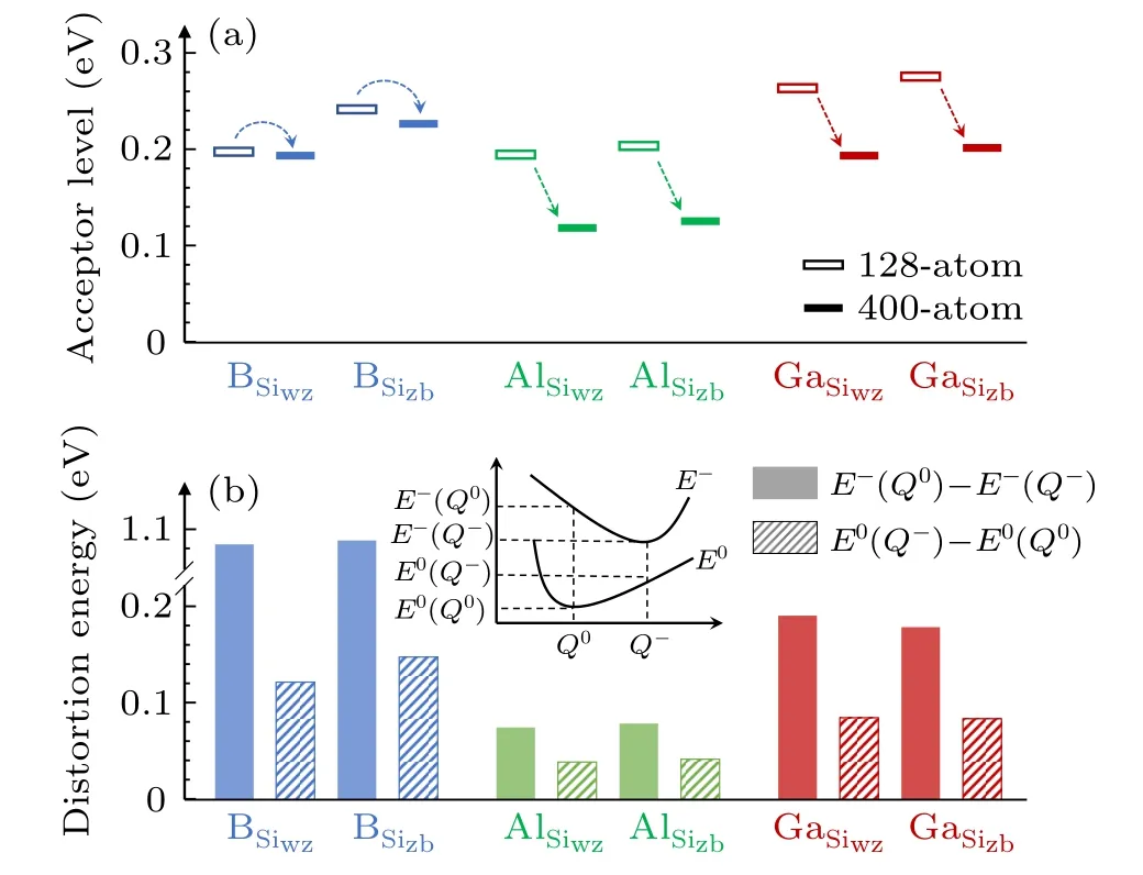
Fig.5.(a)Comparison of theε(0/−)levels calculated using the 128-atom and 400-atom supercells.(b)Distortion energies calculated using the 400-atom supercell between the relaxed structures in the neutral and 1−charge states,denoted by Q0 and Q−,respectively.The distortion energies between the two structures in the neutral(E0)and 1−(E−)charge states are different and shown by shaded and filled bars,respectively.The inset illustrates the involved quantities.For all defects,the most stableΔ1 distortions were used.
Table 1 shows the comparison of the relaxed bond lengths from the 128-atom and 400-atom supercells.For theΔ1and Δ3distortions,the differences between the results from the two supercells are about 0.01A˚ or smaller.However,for the Δ2distortion the difference is large with the largest one about 0.1A˚.In theΔ2distortion,the dopant atom is displaced along the[0001]direction.In the 128-atom supercell,the length of the supercell along the[0001]direction is c=10.043˚A,which is relatively small and results in large differences in the relaxed bond lengths.The bond lengths in the 1−charge state do not show differences(within 0.001˚A)when relaxing from the initial structures of different distortions.Therefore,in Table 1 we only show one set of bond lengths for the 1−charge state.Another observation from Table 1 is that theΔ1distortion is close to C3vsymmetry(or pseudo-C3v),i.e.,the C1–D bond is significantly longer than the other three C–D bonds,which have similar bond lengths.TheΔ3distortion is close to C2vsymmetry,i.e.,the C0–D bond and C1–D bond have similar bond lengths,which are shorter than the C2/3–D bonds.
As shown in Fig.5(a),increasing the supercell size gives rise to shallowerε(0/−)levels.Even though we cannot afford calculations using larger supercells,by analyzing the atomic and electronic structures it is possible to conclude that these ptype dopants are not hydrogenic defects.First,the deep-level defects are associated with large structural distortions as discussed above.The distortions can be quantified by calculating the energy difference between the structures of the neutral and 1−charge states,as shown in Fig.5(b).The distortion energies in the neutral and 1−charge states are calculated by E0(Q−)−E0(Q0)and E−(Q0)−E−(Q−),where Q0and Q−represent the relaxed structures in the neutral and 1−charge states,respectively.[33]For B on the Si sites,the distortion energy can be over 1 eV.Al on Si sites exhibit the smallest distortion energy,which is consistent with results in Fig.5(a)that Al gives rise to the shallowestε(0/−)level.
Figure 6 shows the partial charge density plots of the defect states for B,Al and Ga on Siwzsite.It can be seen that B indeed produces the most localized state,while Al produces the most delocalized states.Ga state is between those of B and Al.This trend is also consistent with that on theε(0/−)levels.The shallower level corresponds to more delocalized defect state.For all defects,the localization is more prominent along the[0001]direction.Even for Al,the localization can be clearly seen.On the other hand,along the basal(0001)plane,the delocalization is more prominent.
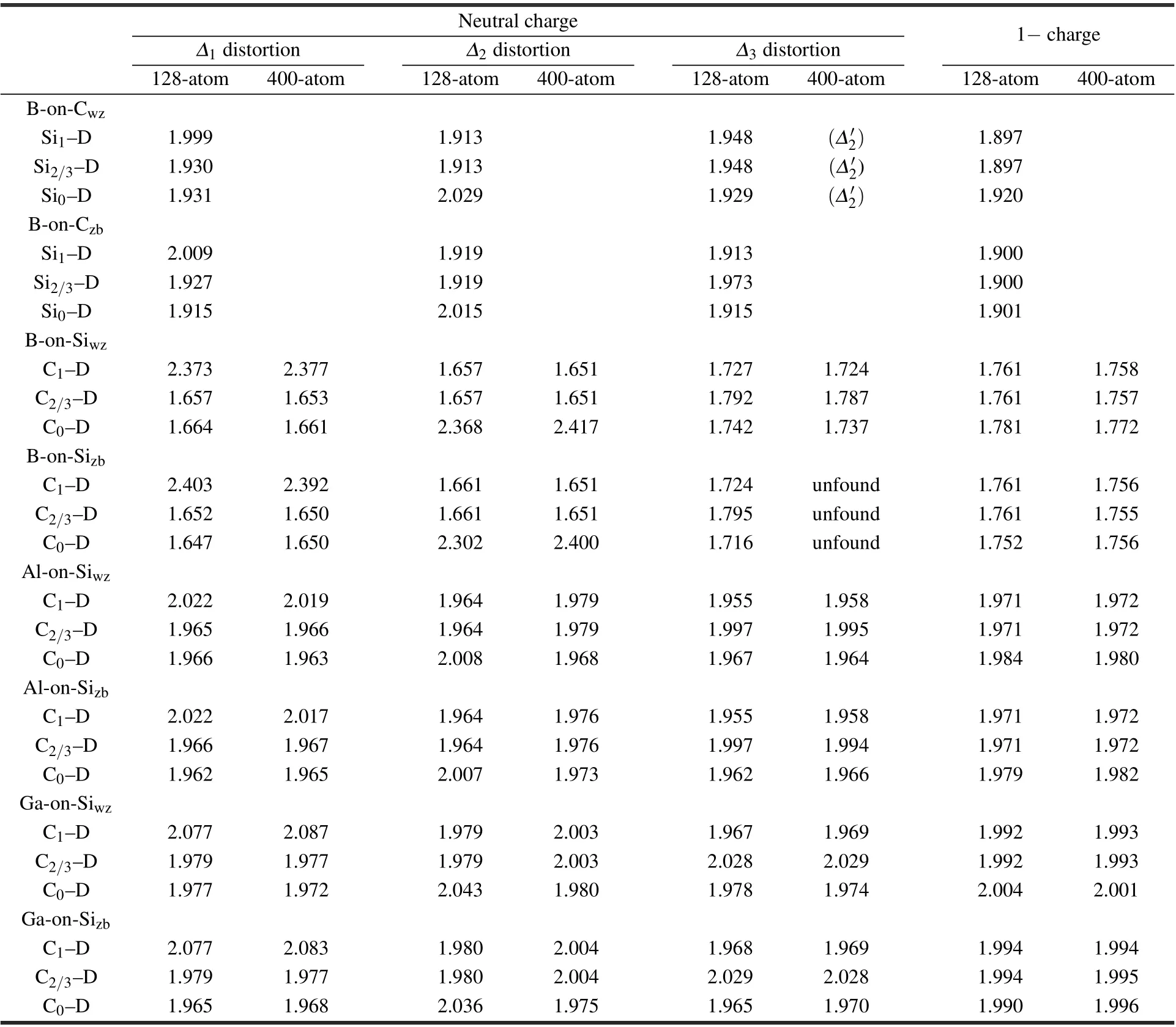
Table 1.Bond lengths between dopant atom(D)and neighboring Si or C atoms in neutral and 1−charge states obtained by using the 128-atom and 400-atom supercells.In neutral charge state,three distortions are shown,namely,Δ1,Δ2 andΔ3,with the exception of B-on-Cwz,for which the third distortion isΔ′2.For C-site dopants,calculations using the 400-atom supercell were not performed.For B-on-Sizb,theΔ3 distortion using the 400-atom supercell was not found.
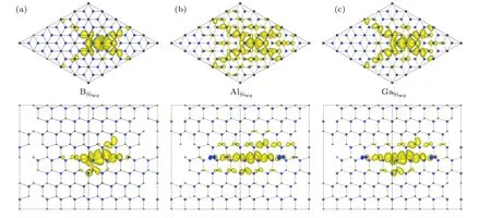
Fig.6.Partial charge density plots of the defect state in band gap for(a)B,(b)Al,and(c)Ga on Siwz site.
4.Conclusion
We carried out a first-principles study on B,Al and Ga doping in 4H-SiC based on HSE hybrid functional.We determined the occupation preference between the Si and C sites and between the wurtzite-like and zincblende-like sites.B could occupy either the Si or C sites depending on the growth condition,while Al and Ga highly prefer the Si sites.All the three dopants do not exhibit significant energy difference between the wurtzite-like and zincblende-like sites.The dopant atoms in neutral charge states are typically stabilized in three different off-center distorted structures.One of them preserves the C3vsymmetry and another two are reduced to Cs(or C1h)symmetry.One of the Csstructures is close to C3vsymmetry and another one is close to C2vsymmetry.As a p-type dopant,Al exhibits shallower acceptor level and lower formation energy on Si sites than B and Ga.All the p-type dopants in 4H-SiC are not hydrogenic.Instead,they all exhibit localized defect states and large distortion energies between the neutral and 1−charge states.In the future dopant engineering,how to utilize the metastable distortions that yield shallower acceptor levels might be worth of study.
- Chinese Physics B的其它文章
- Multiple solutions and hysteresis in the flows driven by surface with antisymmetric velocity profile∗
- Magnetization relaxation of uniaxial anisotropic ferromagnetic particles with linear reaction dynamics driven by DC/AC magnetic field∗
- Influences of spin–orbit interaction on quantum speed limit and entanglement of spin qubits in coupled quantum dots
- Quantum multicast schemes of different quantum states via non-maximally entangled channels with multiparty involvement∗
- Magnetic and electronic properties of two-dimensional metal-organic frameworks TM3(C2NH)12*
- Preparation of a two-state mixture of ultracold fermionic atoms with balanced population subject to the unstable magnetic field∗