
C band microwave damage characteristics of pseudomorphic high electron mobility transistor∗
2021-09-28 02:18QiWeiLi李奇威JingSun孙静FuXingLi李福星ChangChunChai柴常春JunDing丁君andJinYongFang方进勇
Chinese Physics B 2021年9期
Qi-Wei Li(李奇威),Jing Sun(孙静),Fu-Xing Li(李福星),Chang-Chun Chai(柴常春),Jun Ding(丁君),and Jin-Yong Fang(方进勇)
1School of Electronics and Information,Northwestern Polytechnical University,Xi’an 710129,China
2China Academy of Space Technology(Xi’an),Xi’an 710100,China
3Key Laboratory of Ministry of Education for Wide Band-Gap Semiconductor Materials and Devices,School of Microelectronics,Xidian University,Xi’an 710071,China
Keywords:high power microwave,pseudomorphic high electron mobility transistor,damage mechanism,C band,low noise amplifier(LNA)
1.Introduction
With the rapid development of microwave technology,microwave devices are widely used in microwave communication,navigation,telemetry,remote control,satellite communication,and military electronic countermeasures.At the same time,the rapid development of microwave power supply technology makes electromagnetic pulse interference more and more dangerous to microwave semiconductor devices.[1]A large number of simulations and experiments have been carried out to study the electromagnetic immunity of high-power microwave(HPM)at the system or component level.[2–7]
As a typical electromagnetic pulse,narrow-band microwave pulses with a peak power up to several GW and a pulse width of about 100 ns have been reported.[8,9]Such the HPM can be coupled from the front or back doors to disrupt or damage power systems.When irradiated by a strong electromagnetic pulse,the front door coupling through the antenna port will have a large amplitude,especially if the operating frequency band is within the radiation frequency band of the electromagnetic pulse.Therefore,the HPM is considered to be a serious threat to IT infrastructure and communication equipment,especially for radio frequency(RF)front-end components.
In the previous study,Zhang et al.studied the burnt-out characteristics of low noise amplifier(LNA)based on gallium arsenide(GaAs)pseudomorphic high electron mobility transistor(pHEMT)injected with 1.4-GHz microwave pulse.[10]Liu et al.studied the combustion destruction characteristics of Ku band microwave pulses for GaAs pHEMT.[11,12]Yu et al.[13]and Xi et al.[14]studied the nonlinear and permanent degradation of GaAs-based LNA under electromagnetic pulse(EMP).Zhou et al.studied the mechanism of GaN HEMT failure induced by HPM.[15]The C band has good anti-rain attenuation and is often used in satellite communications.However,there are few reports on the HPM effect of C band LNA.
This paper aims to study the damage characteristics of HPM induced pHEMT in the C band from the physical perspective through simulation analysis and the experimental results.The rest of this paper is organized as follows.In Section 2,the simulation model used here is described from three aspects:the device structure,the numerical model,and the signal model.In Section 3,with the help of the device simulator Sentaurus-TCAD,the electric field intensity,the current density,and the temperature characteristics of the device are analyzed to explain the HPM damage mechanism of the device.And we conclude HPM pulse-width-dependent damage rule.In Section 4,the simulation results are compared with the experimental results,and it is determined that the gate region of the pHEMT device is the vulnerable position under the irradiation of C-band HPM.Finally,the conclusions are presented in Section 5.
2.Simulation model
2.1.Device structure
Aδ-doping AlGaAs/InGaAs pHEMT is studied in this paper.Figure 1 shows its basic structure as simulated in TCAD.[16]The device cross-section consists of a 0.8-µmthick GaAs substrate,a 10-nm-deep InGaAs channel,a 34.5-nm-thick AlGaAs spacer layer,a 30-nm-thick GaAs cap layer,and a 50-nm-thick Si3N4passivation layer.There also exists aδ-doping layer,which provides the carriers for the InGaAs channel layer,in the AlGaAs spacer layer.Here,the gate length is 0.15µm and the gate width is 200µm.Furthermore,the gate Schottky barrier height is 0.9 eV and the gate recess is 15-nm deep.The source–gate separation Lgsis 0.575µm including a 40-nm-thick oxide insulation layer for reducing the gate leaking current.Its metal material of electrode is gold.[17]And it is between the source and the drain and its form is symmetric.The area surrounded by the red dotted line in Fig.1 is the vulnerable area inside pHEMT,so the model grid of this area is finely divided,and the research results are given below.

Fig.1.Basic structure ofδ-doping AlGaAs/InGaAs pHEMT.
2.2.Numerical model
To study the physical effect and mechanism of HEMT’s HPM effect,we start from the basic physical equation and use Sentaurus TCAD to construct the physical equivalent model of pHEMT,including the Poisson equation and continuity equation.It is important to consider the electro-thermal effect in the simulation of the burning process of the device injected by the HPM.So the thermodynamic model is adopted to solve the internal physical quantity of the device,and the current density equation of Jnand hole Jpare revised as

whereµn(µp)is the electron(hole)mobilityφn(φp)is the electron(hole)quasi-Fermi potential,and Pn(Pp)is the absolute thermoelectric power electron(hole).Meanwhile,with the thermodynamic model,the lattice temperature is computed from

where cLis the lattice heat capacity,κis the thermal conductivity,k is the Boltzmann constant,ECand EVare the top of conduction band and the bottom of valance band,respectively,and Rn(Rp)is the electron(hole)recombination rate.
Besides,the avalanche model accounting for impact ionization,the analytic-TEP model for thermal electric power,and the high-field-saturation model for electron mobility are also used in this model.[18]The description and physical equation for each of these models are available in Ref.[17].
2.3.Signal model
At present,in the study of the damage effect on the semiconductor device with the HPM event,lots of researchers take the sine wave as the HPM signal model.[19]So the C band HPM is assumed to be a sinusoidal wave without attenuation in this paper,and the mathematical expression is as follows:

where U is the amplitude,f is the frequency,andφis the initial phase.Figure 2 shows the simulation circuit schematic diagram in this study.At first,the drain and the source are applied to with 12 V and grounded,respectively.And by adjusting the resistance R,the HEMT drain potential remains at 2 V when the gate potential is 0 V.Then the sinusoidal wave with a frequency f of 6.6 GHz and an initial phaseφof zero is injected into the gate terminal of pHEMT to simulate the process that the HPM energy couples into the input port of the pHEMT LNA through the front-door path.When the lattice temperature reaches the melting point of gallium arsenide 1511 K,the device is judged to be in failure and the simulation calculation is stopped.
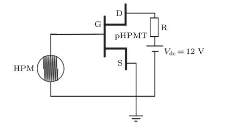
Fig.2.Schematic diagram of simulation circuit.
3.Simulation results and discussion
3.1.HPM damage effect
In the simulation circuit described above,the HPMs with a fixed frequency of 6.6 GHz at different power levels are injected respectively into the gate port of pHEMT to explore the microwave damage characteristics of the C-band of pHEMT.Figure 3 shows the variations of the maximum temperature inside the device with time.Both the temperature change curves show periodic“rising-fall-rising”oscillations.When the HPM power equals 38.55 dBm,the highest temperature inside the device shows an overall upward trend at the beginning,and then the trend of the highest temperature inside the device stops rising and drops slightly,and finally,the trend of the highest temperature inside the device gradually stabilizes.It is inferred that in the last stage of the above-mentioned temperature change,the pHEMT device exchanges heat with the outside and the inside,and thus reaching a thermal equilibrium.Nevertheless,as the power level is elevated to 40.77 dBm,the highest temperature inside the device sharply rises and quickly reaches 1511 K(the GaAs melting point).So it can be inferred that device burn-out may occur.
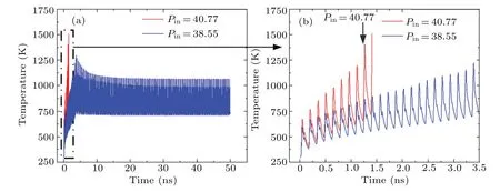
Fig.3.Variations of maximum temperature within pHEMT with time.
Here,the situation that HPM with power of 40.77 dBm is injected into pHEMT is taken for example.Figure 4 shows the temperature distribution inside the HEMT at the time of the device burning down.In Fig.4,the change from dark blue to deep red represents the internal temperature of the device varying from 295.6 K to 1531 K.It can be seen that the hightemperature region represented by deep red is concentrated on the side of the source pole below the grid of the device,and this high-temperature region is called the hotspot inside the device.The formation mechanism of the hotspot is described below.

Fig.4.Distribution of temperature(in unit K)at pHEMT burning time.
3.2.HPM damage mechanism analysis
According to Fig.3(b),the maximum temperature inside the device increases and decreases periodically,and the cycle frequency is consistent with the HPM frequency.In the following the changes of internal physical quantities of the pHEMT device during the single-cycle HPM are analyzed.Figures 5–8 show the data sampled at 0.87 ns and 0.95 ns from the simulation and the temperature distribution,electric field distribution,current distribution,and impact ionization,respectively.The values 0.87 ns and 0.95 ns are the minimum and maximum temperature peaks of the internal maximum temperature of the pHEMT device in an HPM cycle,respectively.Also,the value 0.87 ns is in the negative half cycle of the HPM and the value 0.95 ns is in the positive half cycle of the HPM signal.
Figures 5(a)and 5(b)illustrate the distribution of temperature at 0.87 ns and 0.95 ns respectively.Obviously,the hotspot inside the device is always on the side of the source pole below the gate.And centered on the hotspot,the surrounding temperature decreases gradually.It means that the hotspot occurs where the heat is generated inside the device.However,the hotspot temperature at 0.95 ns is significantly higher than that at 0.87 ns.Therefore,the heat generated by the hotspot also varies in a single HPM cycle.
Combining the heating curve of the pHEMT injected into HPM and the internal temperature distribution of the device,it can be obtained that the internal temperature of the device has an upward trend when the pHEMT gate is injected with HPM.And high temperature area is diffused because the heat generation is greater than the thermal diffusion in the pHEMT device.As a result,there appears a thermal accumulation effect in the device.Moreover,a large amount of heat is continuously generated and accumulated at the hotspot,which will eventually even cause a so high temperature inside the device that it exceeds the melting point of the material,and thus causing the device to burn.However,when the injected HPM power is less than a certain threshold,the internal temperature of the device will not rise any more after reaching a certain value,but will eventually stabilize.This is because the thermal diffusivity of the material increases with the temperature rising.Finally thermal output and thermal diffusion inside the device are balanced.
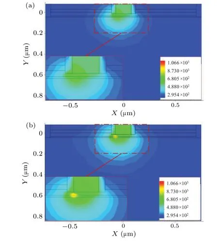
Fig.5.Distribution of temperature(in unit K)at(a)0.87 ns and(b)0.95 ns.
As can be seen from Fig.6,the electric field intensity is very high below the gate of the device,especially on both sides of the gate.This is due to the structure of the device,where the curvature is small,it is easy to form a large electric field intensity.At 0.87 ns,the maximum electric field intensity under the grid is close to that of the drain,while at 0.95 ns,the maximum electric field intensity under the grid is close to the electric field intensity of the source,because there is bias voltage at the drain.
In Fig.7(a),at 0.87 ns,that is,in the negative half cycle,the current density is not large due to the reverse bias voltage of the Schottky junction.It can be seen from Fig.7(b)that at 0.95 ns,which is in the positive half cycle of the HPM,a current path appears under the gate and connects the gate to the InGaAs channel,and the current path is closer to the source side than to the drain.This is because the drain voltage is biased at 2 V,the gate/source voltage is greater than the gate/drain voltage.[20]The research shows that the heatproducing transistor can be expressed as Q=J·E by J current density and electric field intensity E.

Fig.6.Distribution of electric field intensity(in units of V/cm)at(a)0.87 ns,and(b)0.95 ns.

Fig.7.Distribution of current density(in units of A/cm2)at(a)0.87 ns,and(b)0.95 ns.
Therefore,a lot of heat is thought to be generated in the positive half cycle.The area of high electric field intensity and high current density in the positive period device is located below the gate near the source,consistent with the location of the hotspot of the device.This indicates that the energy of HPM coupling into the device is converted into heat,causing the device to burn down.
Figures 8(a)and 8(b)show the distribution of impact ionization at 0.87 ns and 0.95 ns of the device,respectively.The areas with impact ionization rate(in units A/cm2)less than 1×1027inside the device are shown in dark blue,and areas with impact ionization rate ranging from 1×1027to 1.2387×1032are shown in the areas from dark blue to deep red.In Fig.8(b),during the positive half cycle,the deep red area with a high ionization rate is concentrated in the lower part of the gate,and the position with the maximum ionization rate at the lower part of the gate is on the side of the source pole,which is consistent with the position of the large current channel in the lower part of the gate.However,during the negative half cycle,there is no high impact ionization region similar to the scenario during the positive half cycle in Fig.8(a).This indicates that in the positive half cycle,the grid Schottky junction is positively skewed,and the extremely strong grid field leads to an avalanche multiplier effect.In other words,the large forward bias voltage causes the gate to break down,forming a large current channel from the gate to the channel.In the negative half period,the gate/source and gate/drain voltages mostly fall on the reverse bias Schottky junction during the negative period,thereby failing to produce large collision ionization rate.

Fig.8.Distribution of impact ionization(in units of cm−3·s−1)at(a)0.87 ns,and(b)0.95 ns.
3.3.HPM pulse-width-dependent damage effect
To study the HPM damage pulse width effect of pHEMT,in this paper used is the simulation model established above to inject sinusoidal signals with different voltage amplitudes and a frequency of 6.6 GHz into the input end of the pHEMT.And the simulation circuit setting is consistent with that described in Section 2.The HPM pulse width is calculated by the duration of the injected signal before the equipment burns out.Damage power threshold P is the average power absorbed by the equipment during HPM injection,and damage energy threshold E is the total energy absorbed by the equipment during HPM injection.The simulation results are shown in Fig.9.

Fig.9.HPM damage power threshold and energy threshold versus pulse widthτ.
The results show that with the increase of pulse width,the HPM power threshold decreases and the HPM energy threshold increases.Besides,there is a significant nonlinearity for each of the curves.By curve fitting,the empirical formula to describe the correlation can be obtained as follows:

The above relationship is in line with the empirical formula of PN junction damage under monopulse signal presented by Wunsch and Tasca et al.[21,22]
Figure 10 respectively show the temperature distribution of device with gate power injected at 40.49 dBm,41.71 dBm,and 42.40 dBm at the time of burnout in the above simulation,respectively.Comparing the high-temperature regions represented by the bright colors in Fig.10,it can be seen that the greater the injection power,the smaller the distribution area of the high-temperature region at the time of device burnout.This is because when more power is injected into the device,the device burns out in a shorter time and the heat does not have time to dissipate and is concentrated in a smaller area.It can be considered that the power injected by electromagnetic pulse will not change the mechanism of device burning,but only affect the burning time and the size of the high temperature zone.
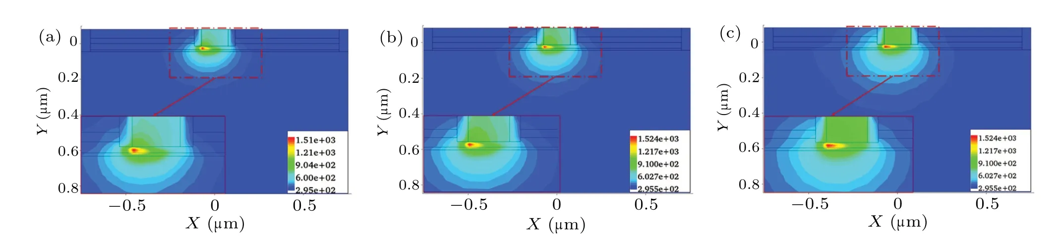
Fig.10.Distribution of temperature(in unit K)when the injected power is(a)40.49 dBm,(b)41.71 dBm,and(c)42.40 dBm.
4.Comparison with experimental results
The experiment is performed by directly injecting a continuous HPM at 6.6 GHz into an LNA.When the injection power exceeds 40 dBm,it is difficult to observe a stable output waveform at the output port of LNA.Therefore,the output gain of LNA is reduced by 20 dBm,which serves as a criterion to judge the damage of LNA.The experimental sample is a three-stage LNA.And the crucial transistors of the first two stages are typical GaAs pHEMT devices,whose gate length and width are consistent with those in the simulation model.By opening the package of the damaged sample,it is found that the LNA damage area is located at the first transistor gate of the LNA as shown in Fig.11.
The scanning electron microscope(SEM)observation results of the first-level damage of the LNA are shown in Fig.12.In Fig.12(a),there are several abnormal locations in the pHEMT device,and the square area surrounded by the red line represents a typical damage area.Figure 12(b)is the magnified view of the square area enclosed by the red line in Fig.12(a).In Fig.12(b),the vertical metal strip in the middle is the gate metal of pHEMT,the left side is the source region,and the right side is the drain region.The gate metal strip is broken.Besides,the channel in the region near the gate is also damaged,and the deviation of the gate to the source side is more serious.[6,10–12]As shown in Fig.12(c),there are small balls and pits formed after the material has melted at the fracture of the gate metal strip.The damage zone of position 1 and position 2 and the normal area are analyzed by EDS,and the results are as shown in Fig.13.

Fig.11.First-stage LNA transistors by optical microscope.
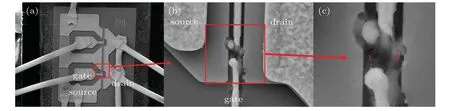
Fig.12.Internal characteristics of damaged samples characterized by SEM.

Fig.13.Energy spectrum analysis of damage at(a)position 1,(b)position 2,and(c)in normal area.
As can be seen from Fig.13,the percentage composition of gold(Au)at position 1(41.45%)and the percentage composition of gold(Au)at position 2(24.68%)are significantly higher than that in the normal area(7.95%).This indicates that the gate metal Au has melted and diffused in all directions.Also,the fractions of nitrogen(5.96%)and silicon(2.78%)at place 1 are both smaller than those of nitrogen(8.61%)and silicon(4.61%)in the normal area.This indicates that the passivation layer between the gate and the source also melts and splashes out.In contrast,the nitrogen component ratio(8.00%)and silicon component ratio(9.00%)in place 2 do not decrease compared with the normal place.It is judged that the passivation layer between the gate and the drain does not burn down or burns not severely.The anatomical analysis results of the above damaged samples are consistent with the simulation results,indicating that the pHEMT will burnt out in the circuit when the HPM power is larger than a certain threshold.Furthermore,the gate of the pHEMT device,especially the gate biased to the side of the source,is the weak link under the action of HPM.
5.Conclusions
The C band HPM damage effects of the pHEMT devices are studied through simulation and experiment in this paper.It can be concluded that the Schottky junction undergoes an avalanche breakdown under the action of a large forward bias voltage,which results in forming a large current.And a large amount of Joule heat generated by the strong electric field and the large current density near the gate forms a hotspot.When the injected HPM power is higher than a certain threshold,the hotspot temperature oscillating rises with time.And pHEMT will eventually damage because of the thermal accumulation at the hotspot.According to the above theory and experimental results,we investigated,the key parameters causing damage to the device under typical pulse conditions,including the damage location,damage power,etc.This work has a certain reference value in evaluating the pHEMT’s microwave damage.
猜你喜欢
音乐天地(音乐创作版)(2021年11期)2021-12-05
短篇小说(2021年10期)2021-06-06
短篇小说(原创版)(2021年10期)2021-01-03
文艺生活·上旬刊(2017年12期)2018-01-10
文艺生活(艺术中国)(2017年12期)2018-01-08
新高考·高二数学(2016年2期)2016-03-07
西江月(2014年4期)2014-03-13
中国火炬(2009年9期)2009-07-24
- Chinese Physics B的其它文章
- Multiple solutions and hysteresis in the flows driven by surface with antisymmetric velocity profile∗
- Magnetization relaxation of uniaxial anisotropic ferromagnetic particles with linear reaction dynamics driven by DC/AC magnetic field∗
- Influences of spin–orbit interaction on quantum speed limit and entanglement of spin qubits in coupled quantum dots
- Quantum multicast schemes of different quantum states via non-maximally entangled channels with multiparty involvement∗
- Magnetic and electronic properties of two-dimensional metal-organic frameworks TM3(C2NH)12*
- Preparation of a two-state mixture of ultracold fermionic atoms with balanced population subject to the unstable magnetic field∗