
Investigations on ion implantation-induced strain in rotated Y-cut LiNbO3 and LiTaO3∗
2021-10-28 07:01ZhongxuLi李忠旭KaiHuang黄凯YandaJi吉彦达YangChen陈阳XiaomengZhao赵晓蒙MinZhou周民TianguiYou游天桂ShibinZhang张师斌andXinOu欧欣
Chinese Physics B 2021年10期
关键词:陈阳
Zhongxu Li(李忠旭) Kai Huang(黄凯) Yanda Ji(吉彦达) Yang Chen(陈阳) Xiaomeng Zhao(赵晓蒙)Min Zhou(周民) Tiangui You(游天桂)Shibin Zhang(张师斌) and Xin Ou(欧欣)
1State Key Laboratory of Functional Materials for Informatics,Shanghai Institute of Microsystem and Information Technology,Chinese Academy of Sciences(CAS),Shanghai 200050,China
2MIIT Key Laboratory of Aerospace Information Materials and Physics&College of Science,N
anjing University of Aeronautics and Astronautics,Nanjing 211106,China
3Center of Materials Science and Optoelectronics Engineering,University of Chinese Academy of Sciences,Beijing 100049,China
4Shanghai Novel Silicon Integration Technology Co.,Ltd.,Jiading,Shanghai,China
Keywords: x-ray diffraction(XRD),implantation,strain,piezoelectric
1. Introduction
With the momentous demand of mobile communication,the new generation of mobile network is introduced approximately every ten years. The fifth-generation (5G) network provides high data rate and extended capacity via accessing higher frequency bands and larger physical bandwidths.[1–6]Compared with 4G LTE,sub-6 GHz 5G network requires improved filter performances such as high frequency,large fractional bandwidth(FBW),low insertion loss,high out-of-band rejection, and excellent temperature stability. However, the low central frequency of the surface acoustic wave(SAW)resonator and the insufficient FBW of the film bulk acoustic resonator (FBAR) are the main challenges of the acoustic wave filters.[7]In recent years, the characteristics of acoustic wave propagating in piezoelectric single-crystalline plate have been attracting attention.[8–11]Micro actuators with a record-high figure of merit were realized on the (YXl)36°cut LiNbO3(LN)thin plate,[12]and the incredible-high-performance SAW(IHP SAW)filters with highQfactor and minimal TCF have been fabricated on(YXl)42°cut LiTaO3(LT)thin film.[8]
Due to the high anisotropy of LN and LT,the large propagation velocity and high electromechanical coupling coefficientsk2are achieved in special orientations,i.e., functional cuts.[5,6,13,14]The ion-slicing technique, combining the crystal-ion-slicing (CIS) and heterogeneous wafer bonding,is one of the mainstream methods of fabricating thin LN/LT plates with versatile orientations.[8–11,15]Ion implantation introduces microscopic defects and strains,[16,17]and the strain profile have a significant influence on the defect evolution and CIS, although it will be disappeared trough a high temperature anneal.[18]The defects and strains of ion-implanted LN were widely investigated by the x-ray diffraction (XRD),but the strain profile in rotated Y-cut LN and LT was less investivated.[19–21]Hence,it remains a lack of the detailed information of desired crystallographic planes changes to investigate the detail information of CIS.
In this work,the strain profiles in ion-implanted(YXl)36°cut LN and (YXl)42°cut LT were investigated. The out-ofplane strain of the (012), (006), and (030) planes were measured through the high resolution x-ray diffraction(HRXRD),and the reciprocal space maps were plotted. A compressive strain exhibited in(030)plane among all the implanted rotated cut LN and LT samples,which is attributed to the large tensile strain in thezdirection of crystal structure((006)plane)after ion implantation.
2. Experimental details
In the present study,the(YXl)36°cut LN was implanted by 160-keV He ions and the (YXl)42°cut LT was implanted by 75-keV H ions.[8,18,22]Both the ion species and the ion fluence are based on the conditions for CIS of LN and LT. The ion implantation was conducted at room temperature and the samples were titled 7°from normal to minimize the channeling effect. The damage profile was calculated using the Stopping and Range of Ion Matter(SRIM 2008).[23]According to the SRIM simulation, the depth of the damage peak is about 530 nm for LN and 570 nm for LT,respectively. The coupledω–2θmeasurements were performed on the(012),(006),and(030) planes to investigate the strain profile using the Philips X’pert x-ray diffractometer. The symmetric and asymmetric RSM scans of(YXl)36°cut LN were conducted to further investigate the strain state.
3. Results and discussion
Owing to the strong anisotropy of single-crystalline LN and LT,SAW devices are fabricated on wafers with particular cut.[24,25]The orientation of the cut is specified by a series of rotations defined by the IEEE standard on piezoelectricity. As shown in Fig. 1(a), thex,y,zandx′,y′,z′represent the coordinate systems of the crystal and the substrate,respectively.Thez′axis of the substrate is rotated 54°counter clockwise around thex(x′) axis for the (YXl)36°LN, and thez′axis of the substrate is rotated counter clockwise around thex(x′)axis 48°for the (YXl) 42°LT. Therefore, the angle between the wafer surface and thezaxis of the crystal is 36°for the(YXl)36°cut LN and 42°for the (YXl)42°cut LT, respectively.LN and LT exhibit a similar crystal structure that can be described with a rhombohedral or a(three times larger)hexagonal unit cell containing 30 atoms.[26–28]The hexagonal unit cell of LN is shown in Fig. 1(b). From the crystallographic structure point of view, the angle between (012) plane and[001] is 36.6°(as the crystal unit cell parameters for LN area=b=0.515 nm andc=1.386 nm)[28]for the(YXl)36 LN.Therefore,the(012)plane can be regarded to be quasi-parallel with the surface of(YXl)36°LN wafer.

Fig.1. (a)An illustration of the relationship between the coordinate system of the material crystal and the substrate structure for(YXl)36° cut LN.The angle between the sample surface and the z axis of LN crystal is 36°. (b)The atomic arrangement in the hexagonal unit cell of LN.The angle between the(012)plane and the z axis is about 36.6°.
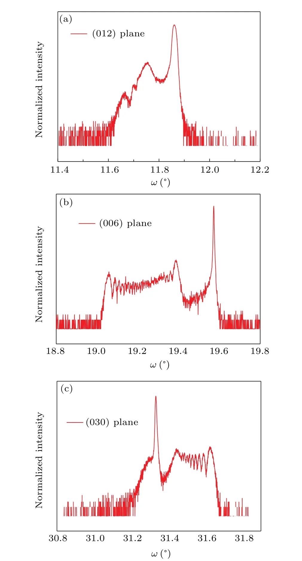
Fig.2.The XRD coupled ω–2θ spectra of the(012)plane(a),the(006)plane(b),and the(030)plane(c)for He-implanted(YXl)36° cut LN samples.
For the rotated Y-cut LN and LT with angleϕ, it is difficult to define a crystal plane which is exactly parallel with the sample surface. Therefore, the (012) planes can be characterized to investigate the out-of-plane strain in(YXl)36°LN. In addition, the HRXRD measurements can be executed on the(030)and(006)planes by tilting the samples with certain offset angles. Theω–2θXRD spectra of the He-implanted (YXl)36°LN are plotted in Fig. 2. The fringe patterns arise from the interferences between scattered beams induced by the damaged part of the crystal, and the fringe spacing is related to the width of the strained region for a given strain level.[29,30]The implantation-induced strain can be calculated according to the Bragg’s theoremεmax=(sin(θ)−sin(θ+∆θ))/sin(θ+∆θ),whereθis the position of the main Brag diffraction peak andθis the distance between the last peak and the main Bragg peak in angle. As shown in Fig.2(a),the interference fringes of the XRD spectrum on the(012)plane extends from the left side of the main diffraction peak,indicating that the interstitial He induces outof-plane tensile strain.[20,21,31]The relative lattice strainε(012)is calculated to be about 1.618% by extracting the distance between the (012) Bragg diffraction peak and the farthest interference fringe. Meanwhile,a set of satellite peaks appear at the left side of the(006)LN main diffraction peak as shown in Fig.2(b),and the relative lattice strainε(006)deduced from the Bragg’s theorem is 2.577%. However, the XRD spectrum on the (030) plane in Fig. 2(c) displays an intriguing strain profile. The main Brag peak is broadened at the left side while a series of satellite peaks exhibit at the right side. It is explicitly that the He ion implantation induces non-uniform strain in the (030) plane and the compressive strain dominates the strain profile. The out-of-plane strain of the(030)planeε(030)is calculated to be−0.837%, in which the minus represents the lattice contraction of the implanted region compared with the undisturbed deeper region.
In addition to the strain gradient of irradiated layer which is characterized along the direction normal to the desired crystallographic plane,a complete description of the strain state of the implanted layer is presented. Figure 3(a)shows the XRD intensity of the symmetric RSM scanning on the (012) plane of the implanted (YXl)36°LN. The positions are located by the in-plane(qx)and out-of-plane(qz)components of the scattering vector,and the intensity is in logarithmic scale. The insert grey solid line represents the coupledω–2θscan of(012)plane. The strong signal (dashed part of the intensity map)corresponds to the main Bragg diffraction of Fig. 3(a) which represents the unirradiated part of the crystal. The spreading of the intensity in the region of higher lattice parameter emerges from the scattering by the damaged layer. Since the 2θ(hkl)/2−ψ(ψrepresents the angle between the(hkl)plane and the surface)of(030)and(006)planes are less than zero for the(YXl)36°cut LN samples,an asymmetric RSM around the(113) diffraction was recorded using the same ion implanted sample. As shown in Fig. 3(b), the two arrows, which share the same starting point located at the maximum intensity corresponding to the undisturbed part of the (YXl)36°cut LN,indicate the values of the in-plane(about 2.385 nm−1)and outof-plane(about 5.082 nm−1)scattering vector components in the substrate.The intensity spreading of the RSM derives from the diffraction caused by the damaged layer. It is noteworthy that the intensity distributions of the symmetric and asymmetric RSM are confined in a sharpqxregion,which indicates that there is no difference between the damaged layer and the substrate. In another words, no deformation occurs in the planes perpendicular to the surface(at least at this low damage level).On the contrary, the wide spread of the intensity along theqzdirection suggests a tensile normal strain in the damaged layer.
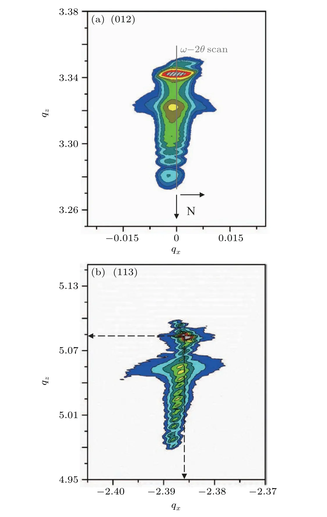
Fig.3. Reciprocal space maps in the vicinity of the(012)Bragg diffraction(a)and the(113)Bragg diffraction(b)of the He-implanted(YXl)36°cut LN.The positions are located by the in-plane(qx)and out-of-plane(qz)components of scattering vector while the intensity is in logarithmic scale. The grey solid line displayed in panel (a) represents a coupled ω–2θ scan. The two arrows in panel(b)represent the values of the in-plane and out-of-plane scattering vector components in the unirradiated part of the crystal.


Table 1. The measured and calculated strain values of different crystallographic planes in LN.


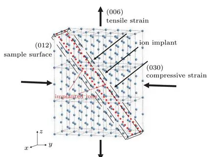
Fig.4. The corresponding crystalline schematic diagram of the strains in implanted(YXl)36° cut LN.To facilitate the presentation of the structure,only the biggest Nb atoms are shown in this diagram, and the red balls represent the implanted He ions.
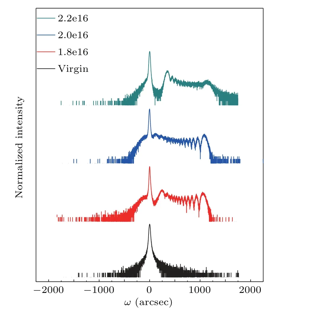
Fig.5. The XRD coupled ω–2θ scan of(030)plane of implanted He ions in(YXl)36° cut LN with different fluence.
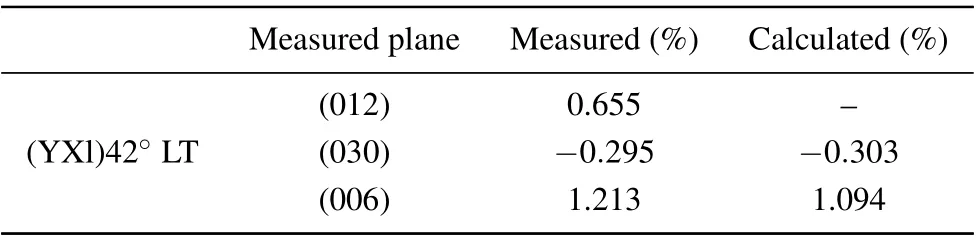
Table 2. The measured and calculated strain values of different crystallographic planes in LT.
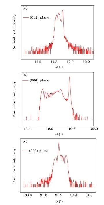
Fig. 6. The XRD coupled ω–2θ spectra of the (012) plane (a), the (006)plane(b),and the(030)plane(c)for H-implanted(YXl)42° cut LT samples.
4. Summary
The understanding of implantation-induced strain is of vital importance to transfer single-crystalline piezoelectric film with various orientations. Here,we investigated the strain profile in the implanted rotated Y-cut LN and LT withω–2θscan and RSM. As the (012) plane is nearly parallel with the surface,the out-of-plane strain is calculated using the XRD spectra measured on the(012)plane.The ion implantation induced tensile strain of the(012)and(006)planes,while the strain of the(006)plane was bigger than that of the(012)plane due to the ion redistribution. From the geometry point of view, the tensile strain of the (012) plane can be regarded as one component of the strain of the(006)plane. Meanwhile,the lattice expansion of the(006)plane induces compressive strain of the(030)plane due to the Poisson effect,while the interstitial ions disturbs the strain profile. This work opens avenues to further understand the ion implantation induced strain in LN and LT for the preparation of POI substrate that seems to best satisfy the requirements for high performance SAW filters in mobile applications.
Acknowledgement
This work was supported by MIIT Key Laboratory of Aerospace Information Materials and Physics & College of Science in Nanjing University of Aeronautics and Astronautics,China.
猜你喜欢
青春期健康(2023年5期)2023-03-18
延河(下半月)(2022年12期)2022-02-01
华人时刊(2021年23期)2021-03-08
好日子(下旬)(2019年9期)2019-07-09
喜剧世界(2017年14期)2017-12-01
故事林(2017年8期)2017-04-25
男生女生(银版)(2016年5期)2017-01-17
民间文学(2014年7期)2014-09-17
Defence Technology(2012年3期)2012-07-25
Defence Technology(2011年3期)2011-07-25

- Chinese Physics B的其它文章
- Physical properties of relativistic electron beam during long-range propagation in space plasma environment∗
- High winding number of topological phase in non-unitary periodic quantum walk∗
- Widely tunable single-photon source with high spectral-purity from telecom wavelength to mid-infrared wavelength based on MgO:PPLN∗
- Control of firing activities in thermosensitive neuron by activating excitatory autapse∗
- Adaptive synchronization of chaotic systems with less measurement and actuation∗
- Dynamics analysis of a 5-dimensional hyperchaotic system with conservative flows under perturbation∗