
Optically-controlled resistive switching effects of CdS nanowire memtransistor∗
2021-11-23 07:29JiaNingLiu刘嘉宁FengXiangChen陈凤翔WenDeng邓文XueLingYu余雪玲andLiShengWang汪礼胜
Chinese Physics B 2021年11期
关键词:凤翔
Jia-Ning Liu(刘嘉宁) Feng-Xiang Chen(陈凤翔) Wen Deng(邓文)Xue-Ling Yu(余雪玲) and Li-Sheng Wang(汪礼胜)
School of Science,Wuhan University of Technology,Wuhan 430070,China
Keywords: CdS,nanowire,memtransistors,optically-controlled,resistive switching
1. Introduction
As the fourth basic circuit element,a memristor was theoretically proposed by Leon Chua in 1971.[1]Until 2008,Strukov and others reported the first working memristor device in Nature.[2,3]Since then,it has become a research hotspot in academia and industry. In the era of big data,the huge amount of information has higher requirements for non-volatile memories.Memristors have been regarded as promising candidates for next-generation non-volatile memories due to their high stack density,high scalability,high durability,ultralow energy consumption and rapid manufacturing processes.[4-7]In 2018,Sangwan first proposed the concept of a memory transistor(memtransistor),[8]which integrated the field effect transistor and memristor into the same device with low-dimensional materials as channels. Rather than the previous memristors,which only respond to a single input, the novel structures can respond to signals from both gate and drain simultaneously. Gate voltage is not only used to modulate the transmission characteristics of field effect transistors,but also used to modulate the resistive switching characteristics of memristors. These forms of storing and processing information are similar to the working patterns of neurons. In addition, some theoretical models are proposed for memristors, for example,a heterogeneous memristive model,[9]multistable memristor model,[10]and so on. The memristor has attracted wide attention in the field of neural network and information security.
In 2019,Yin prepared a novel memtransistor based on 2D MoS2,[11]which can be controlled by both light illumination and gate control. The memristive characteristics of the MoS2memtransistor were subjected to the signals from the drain,gate voltage and illumination,and then the multi-terminal controls of the memristive characteristics were further realized.At present,many 2D layers,for example MoS2[12]and GaSe,[13]and 1-D nanowires, such as MoSe2,[14]ZnO,[15,16]SnO2,[17]CuOx,[18]Cu2S,[19]and so on have been confirmed as channel materials used in memtransistors. All of them achieve a high switching ratio and stable non-volatile characteristics. However,lots of studies only focus on the electrical characteristics and gate voltage modulation of the channel materials,and the optical properties of the channel materials are ignored. Most of the above-mentioned low-dimensional materials also have good optical properties,so it is necessary to explore the optical regulation abilities of low-dimensional materials.[20]
As a 1-D nanostructure, CdS nanowires have excellent optical and electrical properties.[21-23]The direct band gap(2.47 eV) and high photosensitivity of CdS make it very suitable for the detection of visible light.[24-27]Therefore, it has the potential to become the next-generation material for high-performance photodetectors and phototransistors. Similar to CdS, CdSe nanowires were used in optoelectronic devices.[28,29]Some researchers have demonstrated the optical logic gate function in optical effect transistors with CdSe nanowires as channels.[30]The optical switching devices prepared by a single CdS nanowire also have received attention.[21,25]Because of the excellent photosensitivity of CdS nanowires,it is necessary to investigate the optically controlled memristor,which is of great significance for neuromorphic computing applications.[31]Moreover, the 1-D structure can effectively overcome the physical limits of the traditional lithography processes, and can diminish the device size to achieve higher storage density, which means the memristors can be broadly used in micro/nano-devices or chips. The research on memtransistors with CdS nanowires is insufficient.In this paper, a single CdS nanowire was transferred to the silicon wafer by a micromechanical exfoliation method, and then the electrodes were constructed.The current-voltage(Id-Vds) characteristics of the device under light and dark conditions were compared,and the influences of illumination wavelengths and powers on the resistive characteristics of devices were discussed.
2. Fabrication and experimental details
The CdS nanowires were prepared on the Si substrate by the CVD method(Nanjing MKNANO Tech Co. Ltd.),and the length was from 10µm to 80µm. Silicon with 300 nm SiO2wafers were used as substrates and cleaned successively with deionized water,ethanol and acetone in an ultrasonic bath respectively for 10 min. Then the precleaned substrates were cleaned by the RCA standard solution for 20 min and dried with nitrogen flow.
Next, some single CdS nanowires were transferred from the CdS samples to the Si substrate by micromechanical exfoliation method. A single CdS nanowire (length more than 5 µm) was recorded under optical microscope with its location. Using photolithography mask technology, the sourcedrain electrode patterns with a 5µm width channel were prepared.Then a 15 nm Cr film and a 50 nm Au film were successively evaporated on the electrodes by the thermal evaporation technology. The Cr film here was an adhesive layer to make sure that the Au electrodes had good contact with the Si substrate. Finally, the source-drain electrodes were prepared by lift-off processes.
The electrical measurements were performed by using a Keithley 4200 semiconductor parameter analyzer.The heavily doped Si is used as the back gate, while the sweeping range of source and drain voltage is adjusted to observe the current responses. Additionally, the incident light is performed by a CME-OPS1000 tunable monochromatic light source and other lasers. All measurements were performed at room temperature.
3. Results and discussion
3.1. Structure characterization of CdS nanowire device
The typical structure of CdS nanowire devices is shown in Fig. 1(a), where Cr/Au electrodes were prepared as the source and drain of transistors, and the Si substrate as gate.Figure 1(b)shows a SEM image of the CdS nanowire device,

Fig.1. Characterization of the CdS device. (a)A 3-D schematic of the CdS nanowire device structure. (b)SEM image of CdS nanowire device. (c)EDS pattern of the CdS nanowire on SiO2/Si wafer.
where the Cr/Au electrodes are connected to both ends of a single CdS nanowire. According to the bar, the channel between the electrodes is about 5µm,and the length of the whole nanowire is about 14µm. The chemical composition analysis of the nanowire was performed by an energy dispersive x-ray spectroscopy(EDS)technique,as illustrated in Fig.1(c),indicating that the nanowire contains two elements of S and Cd,while the Si and O elements shown in the figure are mainly from the SiO2substrate. The characteristic peak of S is atE=2.35 keV,and the characteristic peaks of Cd are located atE=3.18 keV andE=3.36 keV,respectively.
3.2. Measurement in dark
First,cyclicId-Vdscharacteristics of the device were measured in the dark. The first operation of each sweep is used as initialization, i.e., a positive voltage sweep (0→Vds) is applied to the sample. After that,the applied voltage changes asVds→0, 0→−Vds,−Vds→0, and 0→Vds. As seen from the sweeping curve of−10 V→10 V in Fig.2(a),an obvious bipolar and non-volatile resistive switching behavior can be found. At the initial state,the resistance of device is relatively low, so the device is in the low resistance state (LRS) during the sweeping processes of 10 V→0 V and 0 V→−10 V,then the device switches to the high resistance state (HRS) during the sweeping processes of−10 V→0 V and 0 V→10 V.It is also found that different memristive characteristics can be shown under differentVdssweeping ranges. The switching ratio of the memristor increases with the increase of the sweeping ranges,no matter whether the device is forward or reverse biased. When the appliedVdsis negative, the corresponding current is negative too.For simplicity,all the negative currents are treated by their absolute values.
Further positive/negative voltage sweeps can repeatedly switch the device between the HRS and the LRS for 128 cycles(Fig.2(b)),suggesting reversible bipolar resistive characteristics for the CdS nanowire. At this time, theVdschanges from 10 V→−10 V.Even at the last cycle,the resistances at the HRS and the LRS are very stable,and the switching ratio is as high as 106.
From Fig.2(a),we note that the CdS devices experience the SET process during the higher positive voltage and the RESET process during the lower negative voltage. Generally, a CdS micro/nanostructure has a very large surface-tovolume ratio, and quantities of dangling bonds can induce surface states to exist because of the breaking of lattice periodicity on their surfaces. The carriers diffuse towards the surface and then accumulate there, resulting in band bending upward. Simultaneously, a carrier-depletion region is formed in the vicinity of the surfaces. Although there are differences between the metal work function(5.1 eV)of Au and the semiconductor electron affinity(4.5 eV)of CdS,the surface state of nanowires plays the main role in the formation of the surface barrier.[31]The existence of the surface barrier prevents electrons from moving to the metal, resulting in a higher contact resistance.[24]After applied voltage,the interface between the Au electrode and the CdS semiconductor forms a space charge region. There are some trap states such as vacancies and defects in 1-D CdS nanowires. In the surface space charge region,these trap states can capture and then store carriers,thus adjusting the width and height of the surface barrier.

Fig.2. Measurement results of electrical characteristics of CdS devices. (a)Id-Vds characteristics of CdS with source-drain voltage sweeping in different ranges in dark. (b)Endurance test results.
When a positive voltage sweep(0→Vds)is applied to the sample,due to the existence of a potential barrier,the contact resistance between CdS and the metal eletrode is high; thus,the device is in HRS.As a positive voltage connected to the Au electrode is increased,the carriers injected from the electrodes are captured by the surface defects,which leads to a significant decrease in the height and width of the surface barrier. As the applied voltage increases,more and more deep traps are filled with carriers. The contact between CdS and Au electrode then becomes a quasi-ohmic contact, corresponding to LRS. The injected carriers can stably be filled in the deep level defects and the LRS can be retained even after the removal of electrical bias. The RESET process happens as a negative voltage bias is applied to the Au electrode. The carriers filled in the traps are gradually extracted to the Au electrode. The Schottky barrier becomes higher and recovers to the original state(HRS),so the carriers injected or extracted by the traps in the surface space charge region switch the resistance states of the device.
3.3. Measurement under illumination
Next, CdS nanowires were illuminated with different wavelengths to explore the influences of light illumination.The cyclic sweepingVdsis selected from 10 V to−10 V,and the incident wavelengths change from 400 nm to 1000 nm with 200 nm step. Four differentId-Vdscharacteristics of devices are shown in Fig.3.
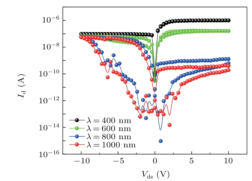
Fig.3. The Id-Vds curves of CdS devices under different incident wavelengths.
It can be seen from Fig. 3 that the incident wavelength can effectively regulate the leakage current of CdS devices under the same source-drain voltage range. If the incident wavelength is lower than 600 nm, theId-Vdscharacteristics of the CdS device are similar to that of a transistor,and there is no obvious hysteresis effect. Meanwhile,when the incident wavelength is over 600 nm, theId-Vdscharacteristics of CdS device change to that of a memristor, and the switching ratio increases with the increase of the incident wavelength. When the incident wavelength exceeds 800 nm, the switching ratio is almost saturated. With the further increase of the incident wavelength, the switching ratio of the device stabilizes in the range of 104to 105, and the current induced by the positive voltage decreases slightly with the increase of the wavelength.
The maximum switching ratios of positive and negative voltages at different incident wavelengths are listed in Table 1.
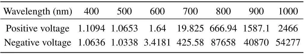
Table 1. The maximum switching ratios of the CdS devices with different incident wavelengths.
It can be seen from Table 1 that when the incident wavelength is 700 nm,the switching ratio of HRS and LRS of CdS nanowires is higher than 10, and CdS devices exhibit obvious memristive characteristics. With the increase of incident wavelength,the switching ratio rapidly increases at first,then nearly saturates.
Based on the above results, two typical incident wavelengths,for example,633 nm and 830 nm,are selected to further discuss the influences ofVdson CdS devices. The measurement results are shown in Fig. 4. Similar to results in the dark,the switching ratio of the CdS device increases with the increase of theVdsrange when the illumination is on. For 633 nm wavelength in Fig.4(a),the switching ratio is over 102when the sweeping voltage is−10 V→10 V. By comparing the results of 633 nm and 830 nm wavelengths,it can be found that the switching ratio under 830 nm illumination is larger and can exceed 105when the sweeping voltage is−10 V→10 V.
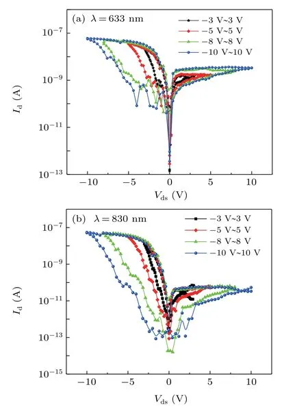
Fig. 4. The Id-Vds curves of CdS devices at different incident wavelengths.(a) The incident wavelength is 633 nm. (b) The incident wavelength is 830 nm.
CdS material is very sensitive to light illumination in the visible light range,[32]so it can be used in photodetectors. By comparing theId-Vdscurves under illumination and in dark conditions, it can be found that the switching ratio is higher in dark conditions. This is because when the CdS is exposed to the ambient air,oxygen is adsorbed on its surface. The adsorbed oxygen will capture electrons from the CdS and form negatively charged ions on the CdS surface,and then a depletion layer with lower conductivity is formed on the surfaces of nanowires.[24,26]Because a 1-D nanowire has an extremely large surface-to-volume ratio, almost all carriers are depleted in the whole nanowire, so the nanowire exhibits a higher resistance in the dark,resulting in a higher switching ratio in the dark. After illumination,part of the oxygen is released,which causes the decrease of the barrier height and the increase of carrier mobility,so the conductivity of the CdS nanowire and the current at HRS increases,which causes the decline of the switching ratio.
As a result,the switching ratio under light illumination is lower than that in the dark. When illuminated with different wavelengths, the optical responses of CdS to different wavelengths are various, and the optical absorption peak of CdS is located between 400 nm and 500 nm. Combining with the results in Fig. 3, we find that when the incident wavelength is 400 nm, the optical absorption of CdS is very strong, so the photogenerated carrier concentration is very high,no matter whether LRS or HRS currents reach the maximum. At this time,carriers can completely cross the surface barrier,then the memristive characteristic of the device disappears, and only the characteristics of the transistor is left. With the increase of incident wavelength,the light absorption of CdS relatively weakens, then the characteristic of memristor is shown, and the switching ratio increases continuously. When the incident light wavelength is 800 nm, the switching ratio reaches the maximum, which is about 105. With the further increase of the incident wavelength, the CdS absorption is weaker at longer wavelength and the measurement results are similar to those in dark conditions,but the currents at the HRS are higher than the results in dark conditions. So,when the incident light wavelength is 1000 nm, theId-Vdscurve is similar to that in the dark.
3.4. Measurement under different optical power
In addition to the influences of incident wavelength and source-drain voltage,the effects of optical power on the resistive switching behaviors of the device are explored.According to the above results,it is found that the device has the highest switching ratio when the incident wavelength is 800 nm;next,the wavelength near this range is used to explore the influences of optical power. A 830 nm laser with adjustable power is selected, and theId-Vdscurves measured under different power densities are shown in Fig. 5, whereP1= 225.5 mW/cm2,P2=70.2 mW/cm2,andP3=18.1 mW/cm2.
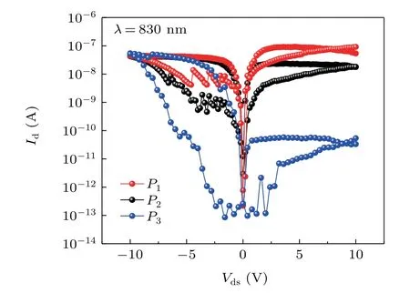
Fig.5.The Id-Vds curves of CdS devices at 830 nm wavelength with different power densities.
In Fig.5,it is found that the optical power also has a significant effect on the device even at the same incident wavelength. The switching ratio at the lower power is much higher than that under higher-power laser. With the increase of optical power, the variation of switching ratio is mainly affected by the current of HRS. That means, when illuminated with a higher-power laser, the generation of photogenerated carriers decreases the barrier height. If a lower-power laser is used,parts of the electrons and holes are recombined, and thus the surface barrier is partially restored. Because the surface barrier has little effect on the LRS, and the current induced by the negative voltage is less affected,the incident laser with the lowest power has the highest switching ratio.

Fig.6. Dynamic photoresponse features of the CdS device. (a)The photoresponse of the CdS device for a 400 nm optical signal modulated with a 1 Hz square wave,and a duty ratio of 3:7. (b)A detailed ON and OFF process of a single pulse.
Finally, a 400 nm pulse laser is used to illuminate the sample to test the photosensitivity of the device. The 400 nm wavelength is chosen because the CdS device has a strong absorption at this wavelength. The period of pulse signal is 1000 ms and the duty ratio is 3 : 7. The waveform of the laser pulse measured by an oscilloscope and the corresponding dynamic photoresponse features of the fabricated devices are shown in Fig.6(a). To check the shape of the laser pulse,a 10 MHz photodector module was connected with a digital oscilloscope to convert the optical signals into electrical signals. It is found the ascending time and descending time of the laser pulse are no more than 20 ms,which is why the laser pulse seems like a square pulse in the upper part of Fig.6(a).Referring to the judgment standards of the response speed of the photodetector,the response speed of the photoelectric device can be reflected by the rising time that the response current rises from 10%to 90%at the moment of illumination and the descending time that the photoelectric current drops from 90%to 10%at the moment when illumination is turned off. In Fig.6(b),the rising time of the response is less than 0.2 s and the descending edge is about 0.3 s.So,the light response speed and recovery speed of the CdS memtransistor are comparable to those of other photodetectors,[31,33]which demonstrates that CdS has a good photosensitivity.
4. Conclusion
In this paper, a single CdS nanowire memtransistor was prepared by the micromechanical exfoliation and photolithography method, and the electrical characteristics of the device were then measured. The CdS device shows a good nonvolatile bipolar memristive characteristics in the dark,and the switching ratio increases with the increment of the sweeping range ofVds, up to about 106. Even after 128 sweeping cycles, the CdS device still maintains a high switching ratio,which proves that the CdS memtransistor has a very superior performance. Because of the photosensitivity of CdS material,the resistive switching ratio of the device can be adjusted by changing the illumination conditions, including the incident wavelengths and the power densities. It is found that the light illumination can be used to control the switching ratio of the CdS memtransistor from 10 to 105,which provides a feasible solution for a multi-terminal controlled memtransistor.By combining the electrical input and optical input, the CdS memtransistor can execute not only data storage but also optical sensing,which is important in the field of multi-terminal synaptic networks.
猜你喜欢
Chinese Physics B(2022年12期)2022-12-28
宝藏(2022年2期)2022-07-30
当代陕西(2021年18期)2021-11-27
辽宁省博物馆馆刊(2020年0期)2020-08-13
中小学校长(2020年6期)2020-08-07
甘肃教育(2020年12期)2020-04-13
当代陕西(2019年23期)2020-01-06
艺术品鉴证.中国艺术金融(2018年8期)2019-01-14
当代陕西(2018年7期)2018-04-26
中国卫生(2016年10期)2016-11-13

- Chinese Physics B的其它文章
- Numerical investigation on threading dislocation bending with InAs/GaAs quantum dots*
- Connes distance of 2D harmonic oscillators in quantum phase space*
- Effect of external electric field on the terahertz transmission characteristics of electrolyte solutions*
- Classical-field description of Bose-Einstein condensation of parallel light in a nonlinear optical cavity*
- Dense coding capacity in correlated noisy channels with weak measurement*
- Probability density and oscillating period of magnetopolaron in parabolic quantum dot in the presence of Rashba effect and temperature*