
Alpha particle detector with planar double Schottky contacts directly fabricated on semi-insulating GaN:Fe template*
2021-11-23 07:30QunSiYang羊群思QingLiu刘清DongZhou周东WeiZongXu徐尉宗YiWangWang王宜望FangFangRen任芳芳andHaiLu陆海
Chinese Physics B 2021年11期
Qun-Si Yang(羊群思) Qing Liu(刘清) Dong Zhou(周东) Wei-Zong Xu(徐尉宗)Yi-Wang Wang(王宜望) Fang-Fang Ren(任芳芳) and Hai Lu(陆海)
1Jiangsu Provincial Key Laboratory of Advanced Photonic and Electronic Materials,Nanjing University,Nanjing 210093,China
2School of Electronic Science and Engineering,Nanjing University,Nanjing 210093,China
Keywords: GaN,alpha particle,detector,double Schottky contacts
1. Introduction
Over the past two decades,wide bandgap semiconductor gallium nitride(GaN)has shown extraordinary application potential in the fields of short wavelength optoelectronic devices and high-power/high frequency devices, such as blue laser diodes,[1]blue to ultraviolet (UV) light-emitting diodes,[2,3]UV detectors,[4]and high-electron-mobility transistors.[5]Meanwhile, it is also generally recognized that GaN could be used for making radiation detectors work in harsh environment due to its wide bandgap energy (~3×Eg,Si), good chemical and thermal stability as well as large displacement energy(~109 eV for N and 45 eV for Ga).[6,7]
Compared with radiation detectors fabricated on conventional semiconductor materials like silicon and gallium arsenide,detectors made of GaN are expected capable of working stably with a long lifetime at elevated temperatures or under high doses of radiation. As summarized in the review paper by Sellinet al., GaN radiation detector could be a competitive candidate utilized in energy spectrum measurement of charged particles, which is applied specifically for the research of fusion process in nuclear reactors or particle physics in special occasions(e.g.,the Large Hadron Collider).[8]Vaiktuset al. fabricated an alpha particle detector with two Au Schottky contacts on 2-µm-thick epitaxial GaN,which gave a charge collection efficiency(CCE)of~92%.[9]Recently,the crystalline quality of epitaxial GaN film is improved steadily and large size free-standing GaN substrate are commercially available. It has been reported that GaN alpha particle detectors with mesa structure or sandwich structure have exhibited high CCE performance of nearly 100%.[10-13]Although GaN alpha particle detectors with planar Schottky structure have been reported in literature, studies on energy resolution and high temperature operation performance of this kind of detectors are very limited.[9,14]It is noticeable that planar Schottky structure has the intrinsic advantages of fabrication simplicity and process compatibility with field effect transistor technology. Another advantage of the planar Schottky structure is the low capacitance,which is important for minimizing RC related transfer delay of electrical signals.
In this work, we have fabricated GaN alpha particle detectors with planar double Schottky contacts(DSC)directly on the semi-insulating (SI) GaN:Fe template grown by hydride vapor phase epitaxy (HVPE). Since undoped HVPE GaN is generally strongly n-type due to impurities or vacancy-related donor centers, the Schottky contact based on it could be very leaky, resulting in high background noise in energy spectrum measurement. An effective approach to enhance the resistivity of HVPE GaN is through carrier compensation by Fe doping.The leakage current can then be reduced down to a sufficiently low level, which allows the detection of weak current pulses induced by incident ionizing particles.
The detectors fabricated in this work are characterized in terms of electrical properties and alpha particle detection performance at both room temperature and elevated temperatures.The main purpose of this work is to evaluate the future application potential of GaN-based planar DSC structure for alpha particle detection with energy resolution.
2. Experiment
The detectors in this work are fabricated on epitaxial Fedoped SI-GaN layer grown by HVPE on sapphire substrate.The SI-GaN layer is 5µm in thick with room temperature resistivity higher than 1×10⁸Ω·cm. Figure 1 shows the crosssectional schematic diagram of the SI-GaN alpha particle detector with DSC.Before the metallization,the samples are degreased and sonicated in acetone,alcohol and de-ionized water for each 10 min,then dipped into dilute hydrogen fluoride solution for 60 s to remove native oxide from the GaN surface. The DSC alpha particle detectors are directly fabricated on the SI-GaN template by using standard photolithography and lift-off techniques. Semi-transparent interdigitated Ni/Au(100 ˚A/100 ˚A)Schottky contacts are deposited on the SI-GaN template via electron-beam evaporation. The designed contact fingers are 10µm wide and 1 mm long with an inter-spacing of 10µm. Subsequently,Ti/Au(2000 ˚A/5000 ˚A)pad layer is deposited on the diagonal margin of the Schottky contacts. For radiation sensitivity characterizations, the processed wafer is diced into individual dies, which are mounted onto TO packages by using conductive silver paste and via wire bonding.
Figure 2 shows the assembled system for energy spectrum measurement of alpha particles. The TO packaged detector is placed within a shielded aluminum cylinder to prevent external electromagnetic interference. An241Am radioisotope source fixed by a polytetrafluoroethylene(PTFE)holder is collimated towards the front surface of the detector. During the detection process,incident alpha particles interacting with the active semiconductor lattice would generate multiple electron-hole pairs,which would be separated and swept towards respective electrodes by junction electrical field. The resulting current pulses are too weak to be measured directly, which have to be fed into a charge sensitive amplifier. The collected charge signals are then converted into linear-tail voltage pulses. The voltage pulse height ∆Vequals toQ/CF,in whichQis the total charge induced by an alpha particle andCFis the feedback capacitor of the charge sensitive amplifier. Thus, the voltage pulse height distribution contains the information of energy deposited by incident particles within the device active layer.The feedback capacitor used in the charge sensitive preamplifier is 1 pF, resulting in a conversion gain of nominally 18.2 mV/MeV for the GaN alpha particle detector. Next, a shaping amplifier(ORTEC 672)is used to shape and amplify the output signals into linear semi-Gaussian voltage pulses.Finally, a multichannel analyzer (AMPTEK MCA-8000D) is used to complete the pulse height counting. During the energy spectrum measurement, the bias voltage applied on the detector is provided by a Keithley 2636A sourcemeter, while an oscilloscope(Tektronix MSO54)is used for the waveform monitoring. The total electronic noise of the detection system is measured by using a Tektronix AFG3102C function generator. A standard ORTEC Si alpha particle detector with a nominal CCE of~100%is adopted for the energy calibration.
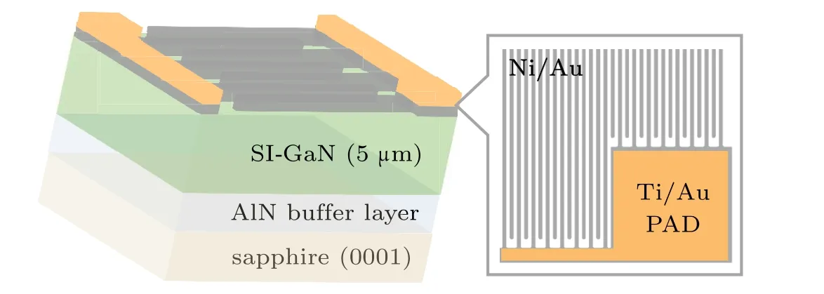
Fig.1. Cross-sectional schematic diagram of SI-GaN based DSC detector.

Fig.2. Schematic of the experimental setup for alpha particle detection with the SI-GaN detector.
3. Results and discussion
The current-voltage (I-V) characteristics of the SI-GaN DSC detector are shown in Fig. 3(a). Since the two Schottky junctions of the detector are back-to-back connected, one Schottky diode is always reverse biased, while the other is forward biased. A good symmetric rectifying behavior can be observed on theI-Vcurve, which indicates that the two diodes have similar Schottky Ni/GaN interfacial barrier properties. Under 10 V bias, the detector exhibits a low roomtemperature dark current of less than 5.0×10⁻¹¹A, corresponding to a linear current density of 5.0×10⁻¹⁰A/cm. Low leakage current is important for energy resolved particle detection, as random fluctuations in leakage current would add electrical noise into the momentary current flow caused by an ionizing event, leading to a significant source of distortion in subsequently processed signals.Figure 3(b)shows the temperature dependentI-Vcharacteristics of the GaN detector plotted in semi-log scale. In the temperature range of 30-90°C,the overall reverse leakage increases at higher temperatures.Meanwhile, at high reverse bias, the leakage current versus bias shows a linear relationship at various temperatures,which suggests that Pool-Frenkel emission is the dominant leakage conduction mechanism.[15,16]

Fig.3. (a)The I-V characteristics of the SI-GaN DSC detector measured in low bias range;(b)the semi-log I-V characteristics of the detector measured at various temperatures.
The energy spectral response of the SI-GaN detector is characterized by using the above-mentioned alpha particle detection system. The alpha radiation source used in this experiment is an241Am radioactive source with an exemption category of V, which has a typical radioactivity of less than 370 kBq. There are four possible alpha-particle transitions during the decay process of241Am. Each kind of transitions involves the emission of alpha particles with different energy and relative abundance, which include 5.389 MeV (1.0%),5.443 MeV (12.5%), 5.486 MeV (86.0%), and 5.545 MeV(0.3%).[17]Since their energies are very close and hard to be distinguished from each other in the energy spectrum,all following calculations conducted in this work are based on the particle energy of 5.486 MeV.The output signal from the GaN detector is firstly fed into the charge sensitive preamplifier and an oscilloscope is used to temporally monitor the amplified signal. A typical pulse waveform excited by a single alpha particle is shown in Fig. 4, which is a fast-rise voltage pulse with an exponential decay back to the baseline. Its rise time and fall time are 0.7µs and 2.2 ms,respectively. Such waveforms are further processed by the shaping amplifier, which has a shaping time set at 2 µs during energy spectrum measurement.

Fig.4. A typical pulse signal of the SI-GaN detector through the preamplifier with a pulse amplitude of ~21 mV.
The alpha particle energy spectra of the SI-GaN detector under various bias voltages are shown in Fig. 5. A double peak structure (“high peak” and “low peak”) is observed in the channels ranging from~1000 to 1900, in which the low peak stays in the low energy direction. During the measurement process, the counting time at each bias is intentionally adjusted so that all high peaks have nearly the same peak heights. It is clear that to reach the same magnitude of high peaks, the counting time has to be reduced at higher bias.Meanwhile,the overall count rate around the low peak drops.This behavior can be explained by the lateral expansion of depletion region within the DSC structure at higher bias, as illustrated in Fig.6. Due to the high resistivity of the SI-GaN,even at a bias voltage of 10 V, the GaN layer between the two inter-digitated contact electrodes is largely depleted, and the depletion layer would reach a maximum depth of 5 µm.Thus, an absence of bias dependence of the peak centroid is observed. As illustrated by the equipotential lines in Fig. 6,the applied bias mostly drops on the reverse biased junction.As bias increases, the width of the lateral depletion region would gradually broaden,until the remaining region between the two electrodes is fully depleted. Meanwhile,some regions outside the contact boundary would also be depleted. During this process,more particles impinging on the detector surface would contribute to effective counts. Thus,the higher the bias voltage, the shorter the accumulative counting time required to achieve a consistent height of the high peaks. In addition,charge collection efficiency should also increase with the rise of bias,which would contribute some high energy counts.

Fig.5. 241Am alpha particle spectrum obtained with the SI-GaN detector at different bias.

Fig.6. Cross sectional schematic of the DSC alpha particle detector during operation. The white arc lines and the dash lines illustrate the equipotential lines below the Schottky electrodes and boundary of the depletion region induced by external bias,respectively.
To further analyze the double-peak characteristics,Gaussian function is used to fit the energy spectrum measured at a bias voltage of 30 V, which gives the energy positions of the peak centroids and their corresponding full widths at the half maximum(FWHM)values. As shown in Fig.7,the low peak can be fitted by Gaussian curve G1,while the high peak can be fitted by Gaussian curves G2 and G3. Apparent peak broadening and count fluctuations of the original spectrum curve can be observed. There are at least three main factors determining the energy resolution(FWHMall)of the detector,which is described by

where FWHMstatis statistical-noise-related spectral broadening caused by the discrete nature of the count signal itself(i.e.,Fano noise),FWHMelecis caused by the random noise of the overall system including the detector and the readout circuit,and FWHMotheris spectral broadening caused by the other factors,such as performance drift of the detector during measurement process and energy straggling in the incident window of the detector.[18]The energy distribution of Fano noise can be described by the following equation:[19]

whereFis the Fano factor,ε0is the average energy required for formation of an electron-hole pair,andEαis the alpha particle energy. By taking the Fano factor of 0.1 andε0of 8.9 eV for GaN, the calculated FWHMstatfor 5.486 MeV alpha particles is~5.18 keV.[20]The electronic noise (FWHMelec) of the entire readout circuit system is tested by feeding periodic short pulse signals produced by a functional signal generator into the circuit,which is determined as~2.3 keV.During the measurement,all parameters of the system are set as same as those used in real energy spectrum measurement. The energy separation between the peak centroids of G1 and G3 is~425 channels,which corresponds to a calibrated energy of 284 keV.Clearly,such a large energy difference between the two peaks can only be caused by FWHMother,which will be discussed in detail later.

Fig.7. Gaussian fitting to the energy spectrum curve of the SI-GaN detector measured under a bias of 30 V.

Fig. 8. Bragg ionization curves of 5.48 MeV alpha particles in gold layer and titanium layer calculated by the SRIM tool.
Considering the special planar structure of the detector,its thick metal pad with an area of 300×300µm2is likely to account for the double-peak characteristics. In this model,alpha particles are emitted radially from241Am radioactive source to the surface of the detector. Some particles falling on the metal pad would inevitably lose certain amount of their energy due to the blocking effect of the pad metal. According to a report by Vigneshwaraet al.,for 5.486 MeV alpha particles vertically passing through a metal layer(500 ˚A Ti/1500 ˚A Au),the average energy loss is less than 110 keV.[21]Figure 8 shows the Bragg ionization curves for 5.48 MeV alpha particles in gold and titanium determined from the stopping range of Ions in matter (SRIM) simulation.[22]Based on these two curves, the average energy loss of 5.48 MeV alpha particles passing through 5000 ˚A Au layer and 2000 ˚A Ti layer are 220 keV and 45 keV,respectively. The sum of these two energies is 265 keV,which is close to the measured energy difference of 284 keV between G1 and G3. Thus,in Fig.7 the G1 peak should be caused by alpha particles passing through the Ti/Au(2000 ˚A/5000 ˚A)metal pad and then depositing energy into the underlying GaN layer, while G3 is caused by alpha particles directly penetrating through the GaN layer. Meanwhile, random interactions of particles and different incident angles would cause energy scattering to a certain extent,which thereby broadens the energy peaks.
Interestingly, the high peak cannot be simply fitted by a single Gaussian curve G3, but a shoulder peak G2 with lower energy has to be combined. The FWHM of the two Gaussian peaks are 117 channels for G2 and 91 channels for G3, respectively. These two peaks are separated by approximately 100 channels, corresponding to an energy of 67 keV. Similar feature has been found in the alpha particle spectra of other GaN-based radiation detectors,[23]but not in SiC-based counterparts.[24,25]In the past studies, it has been well accepted that high-density defect states exist in SI-GaN materials.[26,27]These defect states are caused by dislocations,vacancies,impurities and especially Fe-ion-related compensation centers. Then a reasonable explanation for the shoulder peak is that certain amount of excited carriers are trapped by defect states along their drift path, resulting in an incomplete collection of carriers.[28]Thus, the main energy peak of incident alpha particles would broaden towards its low energy direction in the energy spectrum curve.
As shown in Fig.9,SRIM simulation can also be used to determine the relationship between energy deposition and penetration depth of 5.48 MeV incident alpha particles in GaN,which shows that a total energy loss of 1.48 MeV is deposited within the 5µm SI-GaN.The CCE could be calculated by dividing the experimentally obtained value of energy deposition by its theoretical one(i.e.,1.48 MeV).Meanwhile,energy resolution is of great importance for evaluating the performance of radiation detectors, which is conventionally defined as the FWHM of the energy peak divided by the channel number of the peak centroid.[29]Then, based on the fitting curve with double Gaussian components, it can be determined that the energy resolution of the SI-GaN DSC detector is~8.6% at 1.209 MeV with a corresponding CCE of~81.7%. Thus, it is concluded that the DSC structure is feasible for high energy particle detectors, which provides a simple and low-cost way for radiation detection with reasonable performance. Compared with the traditional vertical Schottky devices with whole electrode, the interdigital approach in DSC design can effectively bring down the proportion of dead region and reduce the energy loss of incident particles.
Finally, to further evaluate the potential performance of the SI-GaN detector, high temperature alpha particle energy spectrum is acquired at 90°C.As shown in the inset of Fig.10,the detector biased at 30 V is heated by using a metal ceramics heater bonded to the back of the TO package,and chip temperature is continuously monitored by a thermocouple mounted next to the detector. By comparing with the energy spectrum profile (gray area) measured at room temperature, it is found that the FWHM of high peak P1 is roughly 235 keV at high temperature, which is almost twice than that at room temperature(see Fig.10). However,little shift of peak energy is observed,which suggests that the GaN detector have potential to operate stably in high-temperature environment.
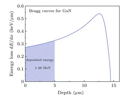
Fig.9. Bragg ionization curve of 5.48 MeV alpha particles in GaN layer.

Fig. 10. Alpha particle energy spectra of the SI-GaN detector acquired at room temperature(~27 °C)and 90 °C.
4. Conclusion
In this work, a planar double Schottky contacts alpha particle detector is directly fabricated on HVPE-grown semiinsulating GaN:Fe template. The detector exhibits low leakage current and is proved capable of detecting partial energies of alpha particles from241Am radioactive source.Distinct double-peak characteristic is observed in the energy spectrum,which is explained by energy attenuation effect of the surface metal pad. The detector exhibits a reasonable energy resolution of~8.6%at deposited energy of 1.209 MeV,and a charge collection efficiency of~81.7% at 30 V bias. The energyresolution limiting factor is found to be the trapping effect of defect states within the SI-GaN:Fe layer, resulting in an incomplete collection of excited charges. The GaN detector also exhibit potential to operate in high temperature environment.This study provides a feasible way to fabricate low-cost and radiation hard GaN-based high energy particle detectors with reasonable performance. To further improve the device performance in terms of energy resolution,thicker SI-GaN layer with improved crystalline quality should be developed.
猜你喜欢
瞭望东方周刊(2022年5期)2022-03-17
水上消防(2021年4期)2021-11-05
重庆与世界(2020年12期)2020-12-23
新少年(2020年4期)2020-05-26
第二课堂(课外活动版)(2019年6期)2019-06-17
第二课堂(课外活动版)(2019年5期)2019-06-17
中国诗歌(2018年3期)2018-11-14
水文地质工程地质(2017年3期)2017-06-21
今古传奇·故事版(2016年21期)2016-12-07
小雪花·成长指南(2015年12期)2015-12-28

- Chinese Physics B的其它文章
- Numerical investigation on threading dislocation bending with InAs/GaAs quantum dots*
- Connes distance of 2D harmonic oscillators in quantum phase space*
- Effect of external electric field on the terahertz transmission characteristics of electrolyte solutions*
- Classical-field description of Bose-Einstein condensation of parallel light in a nonlinear optical cavity*
- Dense coding capacity in correlated noisy channels with weak measurement*
- Probability density and oscillating period of magnetopolaron in parabolic quantum dot in the presence of Rashba effect and temperature*