
Suppression of ion migration in perovskite materials by pulse-voltage method*
2021-11-23 07:32XueYanWang王雪岩HuWang王虎LuoRanChen陈烙然YuChuanShao邵宇川andJianDaShao邵建达
Chinese Physics B 2021年11期
Xue-Yan Wang(王雪岩) Hu Wang(王虎) Luo-Ran Chen(陈烙然)Yu-Chuan Shao(邵宇川) and Jian-Da Shao(邵建达)
1School of Physical Science and Technology,ShanghaiTech University,Shanghai 201210,China
2Laboratory of Thin Film Optics,Shanghai Institute of Optics and Fine Mechanics,Chinese Academy of Sciences,Shanghai 201800,China
3Key Laboratory of Materials for High Power Laser,Shanghai Institute of Optics and Fine Mechanics,Chinese Academy of Sciences,Shanghai 201800,China
4Hangzhou Institute for Advanced Study,University of Chinese Academy of Sciences,Hangzhou 310024,China
5Center of Materials Science and Optoelectronics Engineering,University of Chinese Academy of Sciences,Beijing 100049,China
Keywords: perovskites,ion migration,electrical properties,temperature-dependent resistivity
1. Introduction
Halide perovskite materials have remarkable application prospects in the field of photovoltaic such as solar cells,lightemitting diodes, photodetectors, and radiation detectors due to their excellent light absorption, long diffusion length, high carrier mobility, and low-cost processing.[1-7]Despite the incredible superiorities,the stability of halide perovskite is still challengeable under both environmental conditions and operation conditions.[8]The formation energy of halide perovskite is relatively low so that the perovskite easily degrades under environmental conditions like moisture,oxygen,temperature,UV light,etc. The operation conditions,such as high applying voltage and the bulk injecting current,could also promote the degradation of perovskite devices. Due to the soft perovskite lattice,ion migration is an intrinsic phenomenon in perovskite materials, significantly affecting the current-voltage (I-V)hysteresis and device stability.[9-11]The intrinsic electric properties of the perovskite materials can be obtained accurately when the ion migration is suppressed. The basicI-Vbehavior of the perovskite materials is intricate due to the mixed electronic-ionic characteristic, which is still poorly understood in these semiconductors. Researchers pointed out that ionic conduction is the dominant conduction mechanism of perovskite materials at high temperature.[12]However,the diffusion coefficient of the ion is about six orders of magnitude lower than that of the electron and hole,resulting in a negligible ionic current.[13]The electrical properties of such impressive materials need to be further explored and clarified.
To resolve the above-mentioned issues, various approaches have been introduced to suppress the ion migration.[14-20]Additives and passivation strategies have been introduced to block the ion migration channel at the grain boundary and interface. The ion migration could also be suppressed in low-dimensional perovskites in some reports.[17,18,21]However, these strategies could hinder the intrinsic characteristics of the materials and devices. Developing novel measurement schematic is a promising solution to obtain the intrinsic electrical performance without the interference of ion migration. To the best of our knowledge,there is few reports on suppressing ion migration from the measurement schematic.
The current-voltage measurement is basic yet essential electrical measurements to acquire the activation energy of conductivity,Hall coefficient,carrier mobility,and defect density of materials.[22-24]The traditional current-voltage method is one of the most practical methods, which contains a long voltage duration(t1in Fig. 1(a)) generally above several seconds. Here we call it long duration voltage (LDV) method.There is also another popular electric measurement with short pulse duration of the voltage, which is called pulse-voltage(PV) method in this work. The PV method has been widely used in memristors,[25,26]consisting of the short voltage duration (t1in Fig. 1(b)) and waiting intervals (t2in Fig. 1(b)).Different from the LDV method, the applying duration of a single voltage pulse is on the order of milliseconds to nanoseconds.[25,26]In addition,a PV space-charge limited current procedure was introduced to accurately measure the electronic properties and trap characteristics.[27]Despite the wide application of the PV method, the reasonable implementation of this method is remained to be illustrated. The physical mechanism and effect of the pulse voltage duration are not clear. Moreover,the waiting time between pulse voltages could significantly increases the total elapsed time for measurement. Therefore,a guideline on the parameters of the PV methods should be explored to facilitate the effective implementation.
In this paper, we explore the PV method on methylammonium lead tribromide single crystals to protect the device from the ion migration. Firstly, we analyze the problems due to measurement history during the LDV method. Then, we introduce the PV method intoI-Vmeasurement and discuss the parameter of the PV measurement. A reasonable guideline is summarized to avoid the ion migration in the measurement.The ion migration during the PV measurement is far weaker than that during the LDV measurement. The results attained by the PV method are repeatable, confirming the suppression of ion migration. Moreover,an application of the PV method is demonstrated on the activation energy of conductivity. The activation energy of the single crystal still dramatically reduces around the critical temperature of the cubic-tetragonal phase transition even if the disturbance of ion migration is excluded. By introducing the guideline of the PV method, the measurement history of halide perovskite is under controlled.The intrinsic electrical properties of the perovskite materials can be ultimately revealed under the PV method by suppressing the ion migration.
2. Experiments
The modified inverse temperature crystal growth (ITC)method was applied for the single crystal growth.[28]0.3360 g MABr and 1.1010 g PbBr2were added to 2 ml DMF solvent in 20 ml glass vial and stirred for 6 hours, then filtrated with 0.22 µm polytetrafluoroethylene (PTFE) filter. The solution was heated on a hot plate, raising from 50°C to 70°C at a rate of 2°C/h and kept at 70°C for 6 hours for crystal growth.The MAPbBr3single crystals with the size of 5-10 mm were obtained. The single crystals were fabricated as horizontal devices by evaporating gold electrodes on the same surface at 10−4Pa. The thickness of Au was 80 nm. The single electrode area was 3 mm×1 mm and the electrode spacing was 0.5 mm.
TheI-Vcurves were measured using a Keithley 2400 Series source meter in the dark condition. In the LDV sweeping measurement,the voltage sweep rate was 0.1 V/s in atmosphere. In the PV measurement, unless specified, the single duration(t1)was 20 ms and the waiting interval(t2)was 20 s.More experiment details would be described in the main context. The electric measurement was taken in atmosphere at room temperature 293 K if no special statement in the context. The measurement of the temperature-dependent resistivity was carried out under the vacuum condition of 10−3Pa.The temperature increased or decreased from the initial temperature to the next temperature at the rate of 0.05 K/s. Before each measurement, the device was kept at the measurement temperature for 30 min.
3. Problem in long duration voltage method
Halide perovskites represent a typical kind of soft lattice materials with the composition ofABX3(Ais CH3NH+3(MA+), HN=CHNH+3(FA+), or Cs+;Bis Pb2+or Sn2+;Xis Cl−, Br−, or I−).[1]During the LDV measurement, ions at theAandXsites could migrate significantly under the external field (Fig. 1(c)).[9,29,30]Especially, the halogen ions atXsites are recognized to be movable with the lowest migration barrier. In contrast, the movement of ions during the PV measurement is negligible considering the tiny diffusion coefficient and short voltage duration(Fig.1(d)).
The LDV method is a basic and popular method in various electrical measurements. Many physical properties of materials, such as conductivity, carrier mobility, defect density, etc.can be obtained by this traditional measurement.[24]For some electrical doping materials,such as halide perovskite,the LDV measurement will change the physical characteristic of the materials,forming a measurement history.[31]The ion migration is significantly affected by the scanning rate and direction in the LDV method.[32,33]The ion migration can affect the dark current through the following four aspects. Firstly, ions can produce a negligible drift current far smaller than the electron or hole current since the ion mobility is several orders of magnitude lower than the electron and hole mobility.[34]Secondly,the ions drifted from the lattice sites can form Frenkel defects or interstitial-vacancy pairs. These defects will increase the carrier concentration and promote the vacancy-assisted diffusion.[11]Thirdly, the ions can migrate directionally and redistribute under the electric field,which can form a built-in electric field and shield the external field.[9]At last,the drifted ions can accumulate near the electrode and form an energy barrier,preventing the subsequent carrier injection of the electrode(Fig.1(c)).[35]Therefore,the measured current generally does not show a constant behavior for the sample with obvious ion migration although the applied voltage is constant.
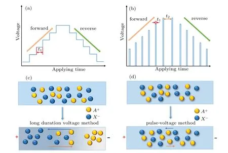
Fig.1. Schematic illustration of the principle and effect in the LDV and PV measurements. (a)LDV method. (b)PV method. The voltage duration and waiting interval are labeled as t1 and t2,respectively. (c),(d)Ion distribution before and after measurement with(c)LDV and(d)PV methods.
Firstly,the horizontal device was measured with positive 15 V for 600 s by the LDV method. As shown in Fig.2(a),the current rises rapidly in the first few seconds and the growth rate of the current slows down gradually. Lately, the current reaches a short-term equilibrium and then gradually decreases at a very slow rate. A certain concentration of vacancies and interstitial atoms are distributed in the as-grown crystal,providing the background carrier density. The current increase probably relates with the increase of carrier concentration from the interstitial defects of Frenkel pairs in the initial stage of ion migration. Once the voltage is applied,more Frenkel pairs are produced. The ionization of shallow levels from the interstitial defects is very fast at the room temperature,whereas the diffusion of ions depends on enough concentration of vacancy defects. The shielding effect of ion migration is more and more obvious until the ion distribution saturates and stabilizes,which requires a relative longer applying duration of voltage.A balance could be observed between carrier increase and shielding effect after sufficient migration of lattice ions. Finally, the shielding effect due to ion migration will be dominant after long poling.
The characteristic of the device has been changed by the measurement history. TheI-Vcharacteristics shows quite different features under subsequent LDV measurements with constant voltage.The ion migration corresponding to long poling of 15 V forms a saturated ion distribution. The device was measured under 10 V for another 600 s after 10 V poling. The applied electric field cannot produce further ion migration so that the current quickly reaches stable(Fig.2(b)). The device was measured under 20 V for another 600 s after 10 V poling. Under the higher 20 V,the current rises rapidly again and then drops slowly,which is attributed to the additional ion migration under the stronger electric field (Fig. 2(c)). Through the time-dependent current curve,we can reveal the defect increase and shielding effect caused by ion migration in the LDV method.
After poling by 15 V,10 V,and 20 V,the horizontal sample shows negligible current difference among repetitiveI-Vsweeping at a fixed scan rate due to the saturated ion distribution (Fig. 2(d)). Compared with that of the as-grown device, the hysteresis area is greatly reduced (Fig. 2(e)). To explore the reversible of ion migration, the device was applied with negative 20 V.The hysteresis of theI-Vcurves due to ion migration occurs again with the LDV method, showing the reversible of ion migration (Fig. 2(f)). Through the above experiments,we emphasize that the LDV method could change electrical properties and form measurement history in halide perovskite materials and devices. In other words, the measurement history of perovskite materials will have a great impact on the performance of subsequent measurement.[36,37]The measurement result is affected not only by the applied voltage but also by the measurement history. The mobile ions during measurement can disturb the electronic current extraction and the underlying fundamental electronic properties of the perovskite materials.
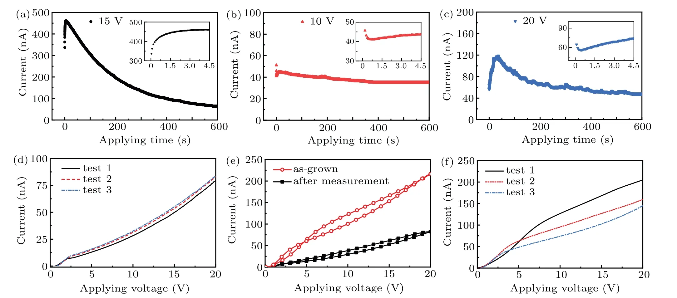
Fig.2. Current curve with the LDV method in the atmosphere. (a)-(c)Time-dependent current curve under the applying voltages of(a)15 V,(b)10 V,and(c)20 V for 600 s duration,respectively. The measurements are taken in the order of(a),(b),and(c). (d)Repetitive I-V curves sweeping from 0 V to 20 V.(e)Hysteresis of the as-grown device and the device after measurements. (f)Repeatability after −20 V applying.
4. Pulsed-voltage method
The PV method has been proposed as an alternative to the LDV method.[27,38]The voltage duration is transient and only from several nanoseconds to milliseconds,which differs from the LDV method. The short-duration voltage significantly weakens and shortens the displacement of ions to control the ion migration. We will prove that the PV method will not cause notable ion migration in materials and devices by choosing appropriate measurement parameters.
Another as-grown device was used to explore the parameter selection of the PV method. Figure 3 shows the ion migration at various constant voltages for one second. Nevertheless,the readout speed of the current is much faster than that of the general LDV method. The readout interval of the current is only 20 ms and the data is stored in the buffer memory until the finish of measurement. The high-resolution current evolution enables us to observe the initiation time of ion migration.The current pumped by 5 V almost remains a low level in the initial 200 ms and increases rapidly after 200 ms due to the ion migration(Fig.3(a)). The time required for the current to rise significantly is reduced from 300 ms to 80 ms when the voltage increases from 5 V to 20 V(Figs.3(a)-3(d)). We first assume that the distance(di)of ion migration should be greater than a minimum value(dmin)corresponding to the perovskite lattice constanta. For convenience of calculation, we assume thatdminis/2 as the edge of[PbX6]octahedron.[10]Ions could not climb over the energy barrier ifdiis shorter thandmin. In this condition,the ions should recover to their original position to keep a minimum energy. The ion mobility in the perovskite was reported about~2×10⁻⁹cm2/(V·s) by Yuanet al.[39]The minimumt1is about 260 ms for thedigreater thandminwhen the applied voltage is 5 V(~100 V/cm for our device).According to the above parameters, the required duration is calculated from 260 ms to 65 ms when the voltage increases from 5 V to 20 V, which agrees well with the experimental values. The above analysis provides a basis for choosing the appropriate pulse duration in the following PV measurements.Therefore,the ions cannot produce effective displacement due to the short applying duration of the PV method.We also measured the instantaneous current evolution of crystals with different initial ion distribution states or different measurement history(Fig.S1). The PV measurement would not change the ion initial distribution or measurement history,but cannot obtain the initial ion distribution. Therefore, we must first discuss the initial ion distribution state of materials or devices before the PV measurement. We performed an instantaneous current evolution measurement at 380 K in vacuum(Fig.S2).Through the measurement,the current is almost unchanged in one second under the voltage of 5 V, 10 V, or 20 V. The selected parameters are still applicable at high temperature.
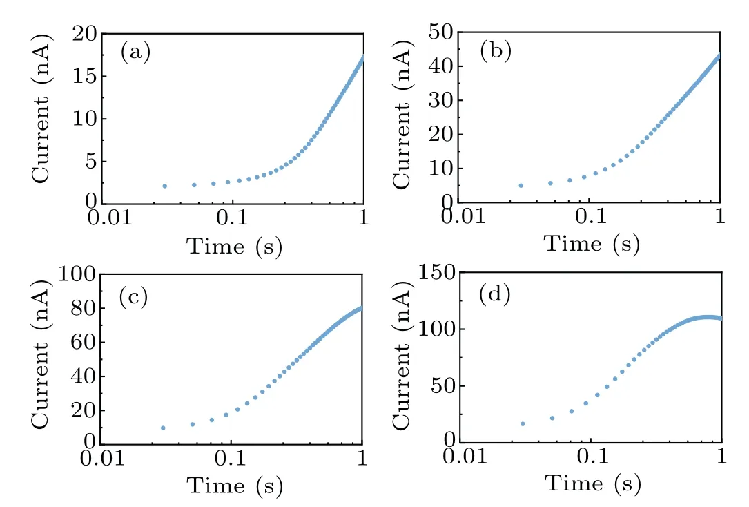
Fig.3. Instantaneous current evolution in the atmosphere. (a)-(d)The current curves under (a) 5 V, (b) 10 V, (c) 15 V, and (d) 20 V, respectively. The current is readout with 20 ms interval.
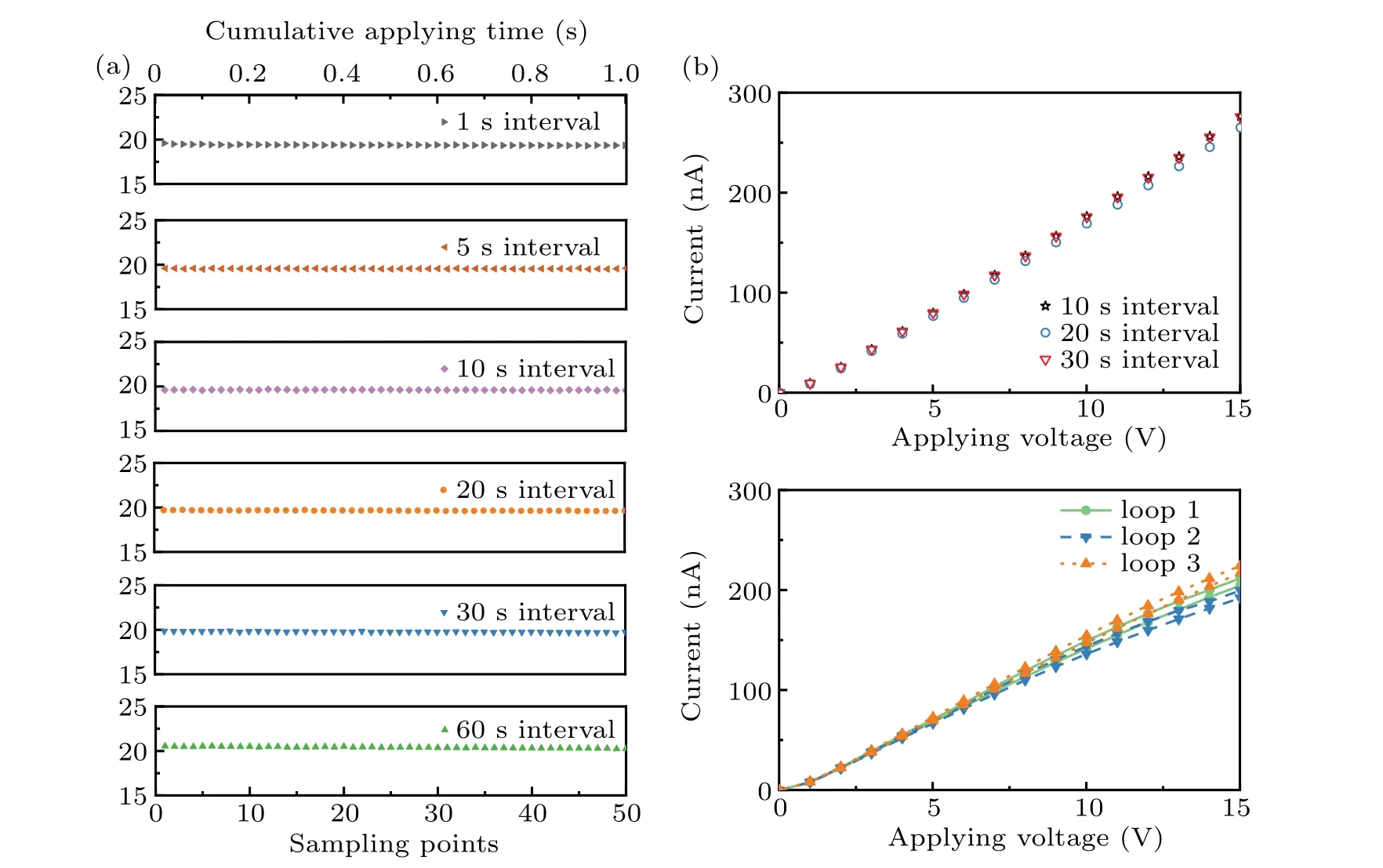
Fig.4. Repeatability of the PV method in the atmosphere. (a)Repeatability of constant voltage with multi-pulse measurement. Each measurement has 50 pulses. The cumulative applying time is 1 s. (b)Repeatability of I-V curve under various waiting interval. (c)Hysteresis of I-V measurement.
To verify the effectiveness of the PV method, different conditions were set to explore the effect of ion migration on electrical properties. Thet1is fixed at 20 ms. The number of sampling points was set to 50 and the cumulative duration was equal to 1 s for individual waiting interval (Fig. 4(a)). The device was applying at constant 10 V with different waiting intervals from 60 s to 1 s. The dark current shows negligible variation in the cumulative duration of 1 s when compared with the measurement in Fig.3. We propose that the ions only vibrate locally at the initial lattice position under the multiple pulses when the pulse induceddiis shorter thandmin. So,theI-Vcharacteristic could show negligible variation. The repeatability of theI-Vcurve with the PV method can be verified under different waiting intervals of 10 s, 20 s, and 30 s(Fig.4(b)). TheI-Vbehavior was also measured three times witht2=20 s(Fig.4(c)). The curve shows negligible hysteresis in relatively low voltage (0-10 V) region. There is still a weak hysteresis among multiple measurements at slightly high range(10-15 V).Nevertheless,the hysteresis obtained by the PV method is far smaller than that by the LDV method.Therefore,a guideline is summarized to implement the PV method reasonably with negligible ion migration, which requires the migration distance to be less thandminfor the combination of voltage duration and applying voltage.
5. Temperature-dependent resistivity measurement
As an application,we demonstrate the PV method in the temperature-dependent resistivity measurement to obtain accurateI-Vcurves without ion redistribution. Since the heating and cooling process required the vacuum conditions, the repeatability ofI-Vcurve was examined in the vacuum conditions for the room temperature, 160 K, and 380 K with the PV method,respectively(Figs.5(a)-5(c)). The measured current in the vacuum is much lower than that in the atmosphere for the room temperature. Although the electrical properties are reported to be sensitive to the environmental gases, the mechanisms and performances are still controversial for the MAPbBr3crystal.[40]The PV method could acquire repeatable and linearI-Vcurves for both low and high temperatures. TheI-Vcurves are fitted linearly to extract the Ohmic resistance. At room-temperature,the resistivity of the singlecrystal device is about 2.3 GΩ·cm. The bulk resistivity of the crystal is higher than the results in other reports.[41,42]It should be noted that the resistivity measurement is affected by many factors,such as device structure,environment,measurement method and parameters. Therefore, different resistivity values could not directly reveal the crystal quality. We suppose that the PV method may not cause additional defects and reveals the intrinsic electric properties. When the temperature decreases to 160 K,the resistivity increases to 23 GΩ·cm(Fig. 5(b)). The resistivity varies rapidly and decreases to 0.06 GΩ·cm when the temperature rises from 160 K to 380 K(Fig. 5(c)). Although the ion diffusion coefficient is reported to be higher at the high temperature,theI-Vcurve is still repeatable with the PV method, validating the PV method in a wide temperature range.
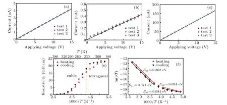
Fig.5. Temperature-dependent resistivity by the PV method in vacuum. (a)-(c)I-V curve at(a)290 K,(b)160 K,and(c)380 K,respectively. (d)Temperaturedependent resistivity during the heating and cooling paths. (e)Activation energy of conductivity from Nernst-Einstein relation.
There is a perspective that the conductivity of halide perovskite is dominated by the drift current of ions at high temperatures due to the Nernst−Einstein relation.[43]Ion migration is frozen in the low temperature region so that the ion conductivity is negligible. Therefore, the electronic conductivity is considered to be dominant by the former researchers in the low temperature region. In our study, the PV method mentioned was used instead of the LDV method to eliminate the influence of ion migration on the temperature-dependent resistivity measurement. The applied voltage was set in the range of 0-15 V and the single pulse duration was 20 ms. The temperature-dependent resistivity of single crystal devices was measured by the heating and cooling paths. Before heating,the device was cooled down to 160 K. The device was then heated to the specified temperature and kept the temperature for 30 min. The highest temperature is 380 K for the heating path. On the other hand, the cooling path implemented the similar workflow except that the specified temperature decreased from 380 K to 160 K.The temperature-dependent resistivity from the two paths is similar in the whole temperature region,excluding the phase transition temperature(Fig.5(d)).During the cooling process, MAPbBr3crystal will change from cubic phase to tetragonal phase and vice versa. The transformation temperature hysteresis is widely observed for a broad phenomenon related with the phase transition.[44-46]Upon heating or cooling,the phase transition cannot finish under one temperature. The cubic-tetragonal phase transition directly changes the band gap and even leads to the formation of ferroelectric domains.[47,48]
The activation energy (Ea) could be extracted from the temperature-dependent conductivity using the Nernst-Einstein relation
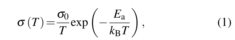
whereTis the Kelvin temperature,kBis the Boltzmann constant andσis the conductivity. In Fig. 5(e), the activation energy is about 0.36 eV along the heating path when the temperature is higher than 230 K. The activation energy is about 0.09 eV when the temperature is lower than 230 K.Similar results can be obtained for the cooling path. In the past studies,the variation of the activation energy for the perovskite materials is related with the ion migration at the higher temperature.[17,49]However,there is still an abruption for the activation energy of conductivity around the transition temperature despite the suppression of ion migration. The result indicates other conductivity mechanisms beyond ion conductivity at the higher temperature. Similar phenomenon can be observed in a previous work with the PV method.[50]The conductivity in the higher temperature can also be affected by the thermal injection,temperature-dependent mobility,and defect density. Depending on the measuring method,the reported activation energy of MAPbBr3single crystal varied significantly.Panet al.attained the activation energy as 0.127 eV by measuring the negative current decay.[42]Mahapatraet al. estimated the activation energy as 0.28 eV by the LDV method.[51]Duijnsteeet al. determined the activation energy as 0.349 eV by the PV space charge limited current method.[50]The activation energies measured by different methods may reflect different physical features. We appeal for a unified guidance to exclude the ion migration and ensure the reliability of universal electrical measurement.
6. Conclusion and perspectives
In summary, we explore the pulse-voltage method on methylammonium lead tribromide single crystals to protect the device from the ion migration. A guideline is summarized through the analysis of measurement history and condition parameters. The influence of the ion migration on the current-voltage measurement, such as repeatability and hysteresis loop,is under controlled. An application of PV method is demonstrated on the activation energy of conductivity. The abruption of activation energy still exists near the phase transition temperature despite the ion migration is excluded by the PV method, introducing new physical insight on the currentvoltage behavior of perovskite materials. The guideline on PV method will be beneficial for measuring halide perovskite materials and developing optoelectronic applications with new technique schematic.

- Chinese Physics B的其它文章
- Numerical investigation on threading dislocation bending with InAs/GaAs quantum dots*
- Connes distance of 2D harmonic oscillators in quantum phase space*
- Effect of external electric field on the terahertz transmission characteristics of electrolyte solutions*
- Classical-field description of Bose-Einstein condensation of parallel light in a nonlinear optical cavity*
- Dense coding capacity in correlated noisy channels with weak measurement*
- Probability density and oscillating period of magnetopolaron in parabolic quantum dot in the presence of Rashba effect and temperature*