
Manipulating metal–insulator transitions of VO2 films via embedding Ag nanonet arrays∗
2021-12-22 06:43ZhangyangZhou周章洋JiaYang杨佳YiLiu刘艺ZhipengGao高志鹏LinhongCao曹林洪LeimingFang房雷鸣HongliangHe贺红亮andZhengweiXiong熊政伟
Chinese Physics B 2021年12期
Zhangyang Zhou(周章洋) Jia Yang(杨佳) Yi Liu(刘艺) Zhipeng Gao(高志鹏)Linhong Cao(曹林洪) Leiming Fang(房雷鸣) Hongliang He(贺红亮) and Zhengwei Xiong(熊政伟)
1Institute of Fluid Physics,China Academy of Engineering Physics,Mianyang 621900,China
2Joint Laboratory for Extreme Conditions Matter Properties,Southwest University of Science and Technology,Mianyang 621010,China
3Institute of Physics,Nuclear,and Chemistry,China Academy of Engineering Physics,Mianyang 621900,China
4School of Materials Science and Engineering,Southwest University of Science and Technology,Mianyang 621010,China
Keywords: vanadium dioxide,volume fraction,Ag nanonet arrays,metal–insulator transition
1. Introduction
Metal–insulator transition (MIT), which is one of the most attractive phenomena in transition metal oxides(TMOs),[1–4]can be driven by various parameters such as element doping,temperature,external pressure,photo-excitation,magnetic field, electric field, and so on.[5–13]The common signature of a phase transition is the sudden change of one or more thermodynamical variables.[9,10]One of emerging parameters of MIT is the control of switchingTcbetween the metal–insulator phases.[8]VO2, as an ideal model system, is metallic at high temperatures and shown a typical metal–insulator structural phase transition at 341 K from rutile structure to monoclinic structure.[11]This dramatic MIT makes VO2potentially useful for ‘smart’ optical and electrical switches,which yet requires the regulation ofTcto around room temperature.[11–15]The mechanism of this MIT has been explained in various ways,such as,localization by the surface scattering, bandwidth narrowing due to the reduced dimensionality, strain, and so on.[15–17]In the past few decades, researchers have made great efforts to solve this problem.[11–18]The most effective route for appreciable reduction ofTcis doping some donor impurity atoms, which could be easily realized by chemical substitution methods, especially tungsten(W6+)with dramatic reduction rates of 20◦C–28◦C per at.%.[7,14,19]The strong interaction between doped atoms and VO2lattices across the MIT induces theTcreduction.[19]Another way to manipulateTcis that metal nanoparticles are embedded into VO2(M) matrix.[20–24]Due to the special local plasma resonance effects (LSPR) of noble metal nanoparticles (e.g.Au and Ag),[21–24]external photon injection brings the resonant absorption of energy, consequently reducing theTc.[25–27]Until now,most research attached importance to the external stimulus of light for theTctuning,[26–28]considering that the MIT nature of metal nanoparticles/VO2system in a lightless environment has as yet received little study. In spite of its importance, however, the underlying physical mechanisms to drive MIT when metal nanoparticles are involved are not well understood. Researchers often study the intrinsic properties of materials in dark environments.[3,5]In view of this issue, it is highly meaningful to explore the MIT of metal nanoparticles/VO2system with a dark environment.
In this study,the Ag nanonet arrays was embedded in the VO2(M) film by polystyrene (PS) template etching approach and electron-beam evaporation method. By changing the volume fraction of Ag nanoparticles in the composites,the phase transition temperature with a dark environment of composite films was studied.
2. Experimental details
2.1. Preparation of VO2 films
The preparation methods of VO2films were reported previously.[23,29–31]In a high vacuum environment, the electron-beam evaporation system was used evaporate the VO2target to grown VO2films(base pressure 5.0×10⁻⁵Pa,working pressure 5×10⁻³Pa). Thin films with 200-nm nominal thickness were grown on quartz (SiO215 mm×15 mm)substrates heated at 300◦C (deposition rate∼0.5 nm·s−1).The optimization of the growth process revealed that a subsequentin-situannealing at 500◦C for 30 min under air atmosphere of 10-Pa pressure was necessary to obtain films with the desired quality.[23]Finally,pure VO2(M)film was obtained and labeled as S0sample.
2.2. Etching PS templates
Close-packed monolayer PS templates were prepared via a modified interface assembly method(Figs.1(a)–1(c)).[32,33]In brief, 0.3-wt% PS sphere dispersion in a 1:1 by volume mixture of deionized water:anhydrous ethanol was dropped slowly on the water/air interface by the drainage glass. Then several drops of sodium dodecyl benzene sulfonate (SDBS)solution (2 wt%) were added to push the floating PS spheres to form an iridescent film, followed by being picked up with SiO2substrates. Subsequently, the close-packed monolayer PS templates were rendered etched to be non-close-packed by a Plasma Pro 80 RIE(Oxford,England)Plasma Etch System performed used a mixture gas of argon and oxygen with 1:5 in pressure and an RF power of 100 W (Fig. 1(d)). The plasma etching duration was 0,200,400,and 500 s to obtain nanonet structures,respectively.
2.3. Preparation of Ag NAs/VO2 composite films
The etched PS templates were placed in a vacuum chamber and evaporated Ag target for 20 min,as shown in Fig.1(e).Then the PS templates plated with the Ag films were immersed in toluene, and the PS spheres were removed by ultrasound.The high-quality Ag NAs with variable periodicity were obtained(Fig.1(f)).Finally,a VO2layer was covered on Ag NAs to obtain Ag NAs/VO2composite films(Fig.1(g)).[23]Based on four etched PS templates(diameter=1080, 862, 647, and 538 nm),the composite films with different Ag sizes were labeled as S1,S2,S3,and S4samples,respectively.
2.4. Characterization
The surface morphology was characterized using fieldemission scanning electron microscope (FE-SEM, Carl Zeiss Supra VP55, Germany) at an accelerating voltage of 10 kV.The crystal phases were identified by thin-film glancing incidence x-ray diffraction (GIXRD, X’ pert Pro MPD, Netherlands) with CuKαx-rays. The electrical switching behavior of the films was studied by using the four-probe system in dismal surroundings which was equipped with a Keithley 2400(Tektronix,America)source meter. The carrier concentration of the samples was measured by Hall measurement system(Nanometrics HL5500PC,America),at room temperature.
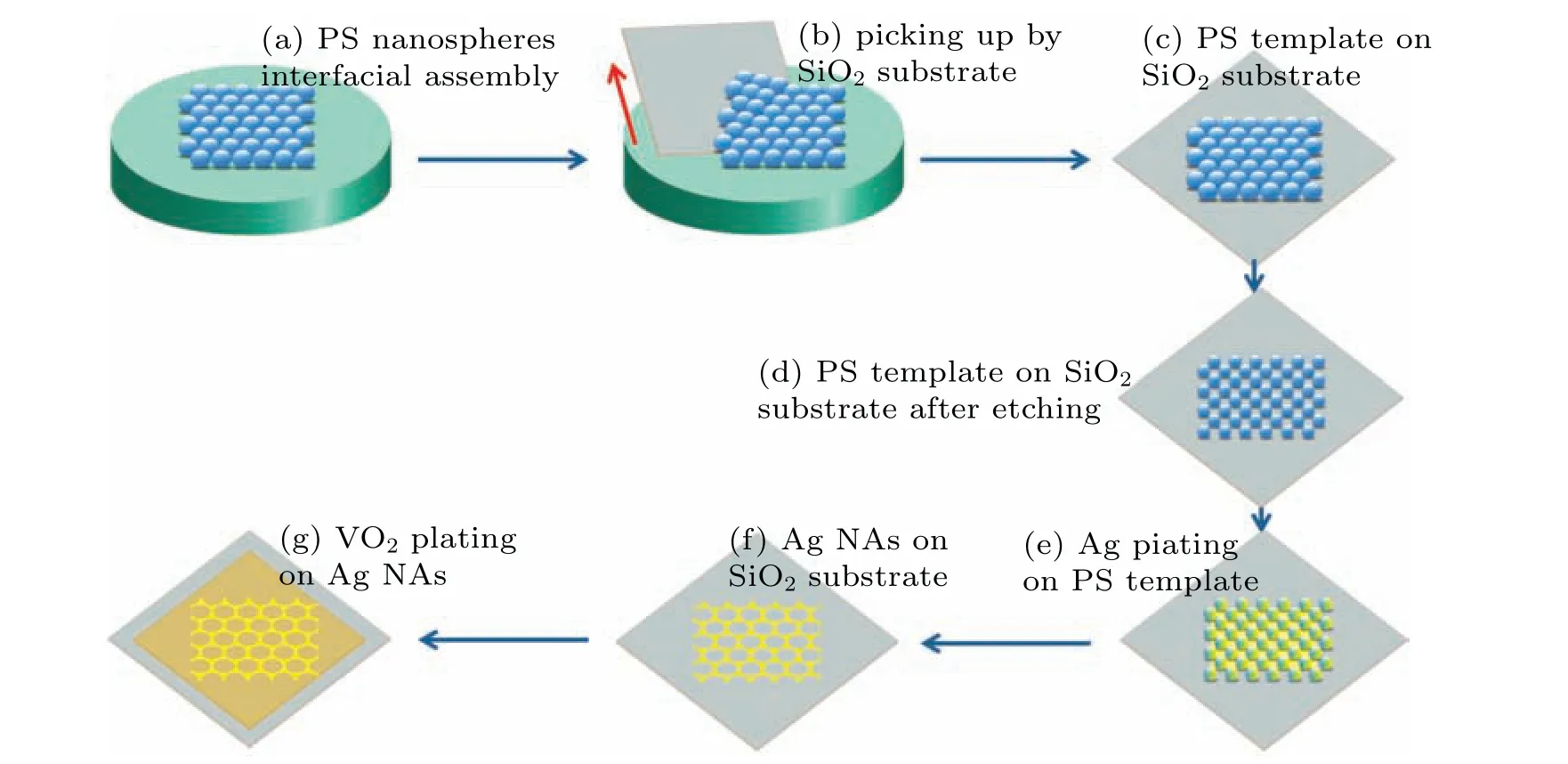
Fig. 1. Schematic diagram of the procedure to made Ag NAs/VO2 composite films: [(a)–(c)] preparation of PS templates, (d) etching PS templates,and[(e)and(f)]fabrication of Ag NAs/VO2 composite films.
3. Results and discussion
Figure 2 shows the GIXRD patterns of the samples measured at room temperature. As depicted,the samples grown at 300◦C exhibit one weak diffraction peak of 2θ ≈25.2◦,corresponding to the crystalline orientation of VO2(B)(110)(space groupC2/m, JCPDS File Card No. 81-2392).[34]Films annealed at 500◦C exhibit strong peaks at 2θ ≈27.9◦,37.1◦,and 55.6◦and are assigned to(011),(211),and(220)orientations of the VO2(M)(space groupP21/c,JCPDS File Card No.65-2358).[14]Except for the VO2(M),no other phase is detectable after annealing. The phase transformation from VO2(B) to VO2(M)is achieved by heating VO2(B)at relatively high temperature to overcome the energy barrier to form the most thermodynamically stable phase VO2(R),which again converts to VO2(M) upon cooling belowTc.[34,35]After embedding Ag NAs,the film exhibited new strong peaks at 2θ ≈38.2◦,44.4◦,and 64.6◦, assigned to(111), (200), and(220)orientations of Ag(space groupFm-3m,JCPDS File Card No.87-0720).[35]A co-existence of both VO2(M) and Ag phases without any impurities is displayed in the composites, revealing the well combination of the two materials.

Fig.2. GIXRD of the samples

Fig. 3. [(a)–(d)] FESEM images of PS templates after Ar/O2 plasma etching for 0, 200, 400, and 500 s, respectively. Inset of panel (a) is the linear relationship of PS sphere diameter and etching duration.
The PS template is a hexagonal close-packed monolayer supported on the SiO2substrate (Fig. 3(a)). The diameter of PS spheres particle is 1080 nm. The inter distance between two adjacent PS spheres is controlled via Ar/O2plasma etching. The average diameters of PS spheres are measured to be 862 (Fig. 3(b)), 647 (Fig. 3(c)), and 538 nm (Fig. 3(d))after plasma etching duration of 200, 400, and 500 s, respectively.At the same time,the PS template still retains the spherical shape after etching, indicating that the etching process is isotropic.[36,37]The hexagonal close-packed structure remains and adheres well on SiO2substrate after the treatment. PS spheres are diminished uniformly and their patterned structures are preserved. The diameter of spheres decreases rectilinear with etching duration with a speed of∼1.08 nm/s measured by SEM(inset of Fig.3(a)). These characters combined with the high reproducibility demonstrate that the plasma etching method is the effective means to precisely control the size of the PS sphere in monolayer colloidal crystal templates.[1,38]
The interspace between the PS spheres is used as templates to produce size-controlled nanonet arrays. Different sizes of Ag NAs are generated by removing PS spheres.[18]As shown in Figs.4(a)–4(d),the high-quality Ag NAs are prepared with variable periodicity,corresponding to PS templates with diameters of 1080, 862, 647, and 538 nm, respectively.Then VO2(M) films were coated on the Ag NAs to form Ag NAs/VO2(M)composites,as shown in Figs.4(e)–4(h),corresponding to S1,S2,S3,and S4,respectively.For embedded Ag NAs,it can be approximately regarded as composed of numerous regular hexagons of equal size(regular hexagon marked in Fig.4).[23]The length of side of the regular hexagon is equal to the diameter of the unetched PS template sphere(1080 nm).At the same time, the particle metrics of the embedded Ag nanonet can be geometrically defined by the corresponding PS templates.[23]In a regular hexagon,the area(S)in-plane of Ag particles can be estimated from the equation

whereR(R= 540 nm) is the radius of PS spheres before etching andris after etching. The height of Ag particles(h=50 nm)should be equal to the thickness of Ag films.[23,36]According to the in-plane area and out-of-plane height of Ag particles,the volume fraction(ϕ)of Ag particles in composite films can be given by
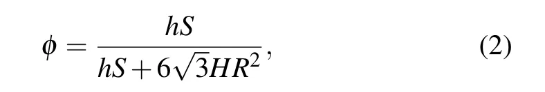
whereH(H=200 nm)is the thickness of the VO2(M)films,andhSis the volume of Ag particles in a regular hexagon.
From formulas(1)and(2),the Ag volume fractions were obtained in Table 1. Obviously,as the particle radius of the PS template sphere decreases from 540 nm to 269 nm,the Ag particles volume and volume fraction of Ag particles increases.Therefore, Ag NAs with a controlled volume fractions were successfully embedded in the VO2(M)films.
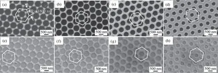
Fig.4. [(a)–(d)]FESEM images of Ag NAs with different sizes,and[(e)–(h)]Ag NAs/VO2(M)composites with different Ag volume fractions.

Table 1. Ag particles volume and volume fractions obtained from PS spheres at different plasma etching durations.
Figure 5(a) shows the relationship between the resistivity and temperature of the samples in a dark environment. In each samples, the phase transition is observed along with the expected hysteresis during cooling.[23]Here,we focus on the the phase transition characteristics with increasing temperature. At room temperature, the samples show semiconductor characteristics and resistivity are about 0.2 Ω/cm–4 Ω/cm.The resistivity drops sharply at about 68◦C with the increase of temperature. A change of nearly two orders of magnitude in the resistivity of the films is observed in a smaller temperature range, indicates that MIT has occurred.[23]At the same time,it is also found that the amplitude of thermal hysteresis loop decreases as the embedded Ag volume fraction increases. These variations are attributed to Ag embedding introduced more free electrons, increases carrier concentration, and thus reduces the resistivity of the material.[39]TheTcvalue was considered to be the center of the thermal hysteresis loop.[22–24]The variation trend ofTcwith Ag volume fraction is shown in Fig. 5(b) (red broken line). Obviously,the embedding of Ag NAs has a significant impact onTc. As the Ag volume fraction increases,Tcdecreases. More specifically, when the Ag volume fraction increased from 0 (S0)to 16.23 % (S4),Tcdecreased from 68◦C to 51◦C. As shown in Fig. 5(b) (blue broken line), the carrier density increases as the embedded Ag NAs volume fraction increases. Specifically,the carrier density increases from 2.58×1018cm−3(S0)to 54.63×1018cm−3(S4) when the Ag volume fraction increased from 0(S0)to 16.23%(S4).The measured carrier density of the pure VO2(M)film is close to the result reported by Zhouet al.,indicating that the Hull measurement is valid.[40]Previous studies had proved that VO2(M) is an N-type semiconductor in which electrons play a leading role in the conduction mechanism.[23,40]So, with the embedded Ag volume fraction increases,the decreasedTcand increased carrier density are due to more free electrons injected into the VO2(M)films.

Fig. 5. (a) Resistivity–temperature curves of the samples, (b) temperature,carrier density–volume fractions relationship of the samples.
This phenomenon was actually confirmed in the 1975s.[41]The increase of free electrons concentration will lead to phase transition at a lower temperature.[23,41]In order to understand more clearly for this phenomenon,we used the changes of energy band with materials Ag and VO2(M)before and after contact to explain,as shown in Fig.6. As depicted in Fig.6(a),the vacuum levelE0as a reference.The work functionWm(4.6 eV)[42,43]of materials Ag is much lower than N-type VO2(M)(Ws=5.4 eV).[43,44]Ag and VO2(M)contact while formed an Ohmic junction,[23]which promotes the electrons transition from high(Ag)to low(VO2(M))concentration until their Fermi levelsEFmandEFsalign,and absorbed energy(WA)at the junction,as shown in Fig.6(b).[44,45]The absorbed energy is proportional to the number of electrons flowing into the semiconductor.[45]For the Ag/VO2system, the energy of phase transition is fixed, the energy provided by the heating system will decrease with the more energy is absorbed,corresponding to cut downTc.[23]The mechanism ofTcreduction in Ag NAs/VO2(M) composites: as the Ag volume fraction increases, more free electrons are injected into the VO2(M)films to generate greater absorption energy at the nanometal–semiconductor junction,thus loweringTc.

Fig.6. Energy band of Ag/VO2. The red solid spheres represent the excited electrons.E0 is the vacuum level.EFm and EFs are the Fermi levels of Ag and VO2,respectively. Ec and Ev are the conduction band(CB)and valence band(VB) of VO2, respectively. Wm and Ws are work functions of Ag and VO2,respectively.WA is the energy absorbed in the contact region when electrons are injected from Ag to VO2.
4. Conclusions
In this paper, we prepared the Ag NAs with controllable periodicity embedded into VO2(M)films via nanosphere lithography. By adjusting the size of the PS nanospheres by changing the etching time, Ag NAs with different volume fractions were obtained in the Ag NAs/VO2(M) composite films. On this based, it was found thatTcdecreased from 68◦C to 51◦C, and the carrier density increased with the increased volume fraction. Combined with the energyband analysis of Ag/VO2(M), the detailed mechanism ofTcreduction was explained that more free electrons injected into the VO2(M) films, the greater the energy absorbed at the nanometal–semiconductor junction.[23]These results provide a reference for controlling the metal–insulators transition in VO2, and have directive significance for the application and development of other strongly correlated materials.
猜你喜欢
新作文·小学低年级版(2022年5期)2022-08-30
Chinese Physics B(2022年4期)2022-04-12
内燃机与配件(2022年2期)2022-01-17
交响-西安音乐学院学报(2021年1期)2021-05-29
开发研究(2020年2期)2020-07-30
Chinese Physics B(2019年7期)2019-08-06
水动力学研究与进展 B辑(2018年5期)2018-10-27
家庭影院技术(2017年8期)2017-10-13
商情(2017年5期)2017-03-30
疯狂英语·新悦读(2017年12期)2017-02-18

- Chinese Physics B的其它文章
- Transient transition behaviors of fractional-order simplest chaotic circuit with bi-stable locally-active memristor and its ARM-based implementation
- Modeling and dynamics of double Hindmarsh–Rose neuron with memristor-based magnetic coupling and time delay∗
- Cascade discrete memristive maps for enhancing chaos∗
- A review on the design of ternary logic circuits∗
- Extended phase diagram of La1−xCaxMnO3 by interfacial engineering∗
- A double quantum dot defined by top gates in a single crystalline InSb nanosheet∗