
High linearity AlGaN/GaN HEMT with double-Vth coupling for millimeter-wave applications
2022-02-24 08:59PengfeiWang王鹏飞MinhanMi宓珉瀚MengZhang张濛JiejieZhu祝杰杰YuweiZhou周雨威JielongLiu刘捷龙SijiaLiu刘思佳LingYang杨凌BinHou侯斌XiaohuaMa马晓华andYueHao郝跃
Chinese Physics B 2022年2期
关键词:杨凌
Pengfei Wang(王鹏飞) Minhan Mi(宓珉瀚) Meng Zhang(张濛) Jiejie Zhu(祝杰杰) Yuwei Zhou(周雨威)Jielong Liu(刘捷龙) Sijia Liu(刘思佳) Ling Yang(杨凌) Bin Hou(侯斌)Xiaohua Ma(马晓华) and Yue Hao(郝跃)
1Key Laboratory of Wide Band-Gap Semiconductor Materials and Devices,School of Microelectronics,Xidian University,Xi’an 710071,China2School of Advanced Materials and Nanotechnology,Xidian University,Xi’an 710071,China3Xidian University Guangzhou Institute of Technology,Guangzhou 510555,China
We demonstrated an AlGaN/GaN high electron mobility transistor (HEMT) namely double-Vth coupling HEMT(DVC-HEMT) fabricated by connecting different threshold voltage (Vth) values including the slant recess element and planar element in parallel along the gate width with N2O plasma treatment on the gate region. The comparative studies of DVC-HEMT and Fin-like HEMT fabricated on the same wafer show significantly improved linearity of transconductance(Gm)and radio frequency(RF)output signal characteristics in DVC-HEMT.The fabricated device shows the transconductance plateau larger than 7 V,which yields a flattened fT/fmax-gate bias dependence.At the operating frequency of 30 GHz,the peak power-added efficiency(PAE)of 41%accompanied by the power density(Pout)of 5.3 W/mm. Furthermore,the proposed architecture also features an exceptional linearity performance with 1-dB compression point(P1 dB)of 28 dBm,whereas that of the Fin-like HEMT is 25.2 dBm. The device demonstrated in this article has great potential to be a new paradigm for millimeter-wave application where high linearity is essential.
Keywords: AlGaN/GaN,linearity,1-dB compression point,millimeter-wave application
1. Introduction
The surging demand for the Internet of things (IoT)has promoted the development of modern wireless communication technologies.[1–3]High data transfer rate and spectrum efficiency have becoming significant index parameters for modern mobile communication equipment in power amplifiers (PAs), which imposes higher linearity requirements on PAs.[4,5]Gallium nitride (GaN)-based high-electron mobility transistors (GaN HEMTs) have been the most promising devices for PAs in telecommunication applications due to superior material properties.[6,7]However, the conventional AlGaN/GaN HEMT suffers from nonlinearities with a bell-shaped transconductance (Gm) profile, which may be attributed to several physical origins including (i) self-heating effects,[8](ii) parasitic capacitance,[9](iii) source resistance nonlinearity,[10–12]and (iv) electron saturation velocity.[13,14]Several approaches have been employed to address theGmroll-off at high drain current level.[15–19]Choi[20]obtained a composite device withGmplateau>6 V and OIP3/Pdcis 8.2 dB at 30 GHz by optimizing the fin width and number of fins along the gate direction. Sohel[21]has reported the polarization-graded transistors by employing a threedimensional electron gas channel (3DEG) with OIP3/Pdcof 13.3 dB at 10 GHz.
Additionally,we have recently proposed a novel architecture with transconductance plateau>5.6 V by tailoring a flatGmprofile.[22]Such structures have been proven to be able to effectively suppress theGmroll-off at high drain current and thus enhance the linearity. However, the off-state current induced by etching is deteriorated about 2 orders compared with conventional planar HEMT, which severely impedes device reliability and deteriorates power efficiency.[23]It has been found that the plasma treatment such as N2O can effectively suppress the leakage current.[24–26]
In this work, we optimized the structure reported in our previous work[22]by connecting differentVthvalues including the slant recess element and planar element in parallel along the gate width with N2O plasma treatment on the gate region. The architecture of such scheme is named as double-Vthcoupling-HEMT(DVC-HEMT).In comparison with Fin-like HEMT, the linearity of DC and RF characteristics has been significantly promoted for DVC-HEMT.The fabricated DVCHEMT shows a gate voltage swing (GVS) of the transconductance plateau larger than 7 V and a constantfT/fmaxof 40 GHz/60 GHz over a wide gate voltage range. Due to the thin oxide layer formed by N2O treatment, the DVC-HEMT demonstrates an on/off ratio of over 108, associated with a maximum current collapse (CC) of as low as 3.2%. At theoperating frequency of 30 GHz, the peak power-added efficiency(PAE)of 41%accompanied by the power density(Pout)of 5.3 W/mm atVd=20 V is obtained by the DVC-HEMT,as well as that of Fin-like HEMT is 34% accompanied by 4 W/mm atVd= 2 V. Furthermore, the proposed architecture also features an exceptional linearity performance with 1-dB compression point(P1dB)of 28 dBm at 30 GHz,whereas that of the Fin-like HEMT is 25.2 dBm. Therefore,the DVCHEMT is believed to be an attractive alternative approach for millimeter-wave application requiring high linearity and high efficiency.
2. Device structure and fabrication
The devices in this work were fabricated on an Al-GaN/GaN heterostructure grown on SiC substructure by metalorganic chemical vapor deposition (MOCVD). Figure 1 shows the schematic of the devices. Its epilayers include a 1.3-µm GaN buffer layer, a 1-nm AlN interlayer, and a 24-nm AlGaN barrier. The measured two-dimensional electron gas (2DEG) mobility and density are 2096 cm2·V−1·s−1and 1.04×1013cm−2,respectively.

Fig. 1. The structure diagram of (a) Fin-like HEMT and (b) DVC HEMT;(c)the TEM micrograph of the surface plasma treatment formed by oxide on AlGaN barrier;(d)process flow for the fabricated DVC-HEMT.
Four different devices including a convention planar HEMT(the inset 1 in Fig.2(b)),recess-gate HEMT(the inset 2 in Fig.2(b)),Fin-like HEMT(as shown in Fig.1(a)),and the DVC-HEMT(as shown in Fig.1(b))were fabricated together for comparison.Device fabrication started with the source and the drain Ohmic contact formation using Ti/Al/Ni/Au evaporation process followed by rapid annealing at 850°C for 50 s in ambient N2. After the device’s electrical isolation was formed through nitrogen ion implantation,an Ohmic contact resistance of 0.36 Ω·mm was achieved and verified using transmission-line measurement (TLM). A 120-nm SiN layer was deposited by plasma-enhanced chemical vapor deposition(PECVD), and electron beam lithography (EBL) was used to define the gate foot. For the detailed information of planar HEMT,recess-gate HEMT and Fin-like HEMT is described in our previous work.[22]
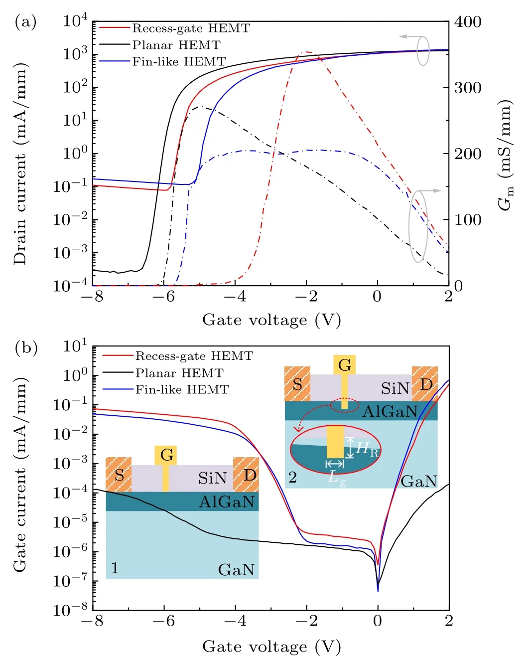
Fig.2. Comparison of(a)transfer characteristics and(b)Schottky characteristics among planar HEMT, recess-gate HEMT, and Fin-like HEMT. Inset:cross section of 1 the planar HEMT and 2 gate-recess HEMT.
Significantly,for the DVC-HEMT as shown in Fig.2(b),after removing the SiN in the gate region, a second EBL lithography was employed to define slant recess. Since SiN served as a hard mask during the Cl2-based etching process,the periodic slant recess features the same length as the gate foot. After that, the gate region was treated by N2O plasma.The N2O plasma treatment was carried out in the PECVD system. The chamber pressure was 600 mTorr (1 Torr =1.33322×10²Pa),the flow rate of N2O was 80 sccm,the ambient temperature was 250°C,the plasma power was 200 W,and the treatment time was 30 min. This process is aimed to form a layer of oxide instead of deposition or thermal growth using additional process. The thickness of the oxide was estimated to be around 3 nm by using the transmission electron microscopy (TEM) image as shown in Fig. 1(c). Finally, a gate cap based on Ni/Au/Ni metal stacks was deposited using electron beam evaporation. The process flow for DVC-HEMT fabrication is shown in Fig.1(d). For a direct comparison,all devices have the same gate length (Lg) of 200 nm, a source drain distance (Lsd) of 3 µm. In particularly, the etch depth(HR) of recess-gate HEMT (the inset 2 in Fig. 2(b)) and Finlike HEMT is 7.5 nm.
3. Results and discussion
The DC measurement of the fabricated devices are measured by Keithley 4200 semiconductor analyzer. Figure 2(a)shows the comparison of transfer characteristics among planar HEMT, recess-gate HEMT, and Fin-like HEMT. It could be notably observed that the GVS(the difference in gate voltage corresponding to 80%of the peakGm)of Fin-like HEMT is significantly improved in comparison with that of planar HEMT and recess-gate HEMT.The flatterGmprofile of Finlike HEMT implies that the architecture can effectively inhibitGmroll-off at high drain current. However, as shown in Fig. 2(b), the off-state leakage current of planar HEMT is at the order of 10−4mA/mm,whereas,that of Fin-like HEMT and recess-gate HEMT is up to 10−2mA/mm. The deterioration of leakage current is mainly attributed to the dry etching which may result in the interface scattering[27]and the increment of tunneling current.[28]
In order to comparatively investigate the DC characteristics of DVC-HEMT,we selected the Fin-like HEMT as reference. As shown in Fig.3(a),due to a thin oxide layer formed on the gate region of DVC-HEMT,the gate leakage current at least 4 orders of magnitude lower than that of Fin-like HEMT,leading to an ultralow off-state current of 9.3×10⁻⁶mA/mm accompanied by an on/off ratio of over 108. Interestingly, a higher RF linearity performance will be manifested for HEMT when the first- and second-order derivatives of transconductance is close to zero,[20]which means that it is key to reduce the derivative characteristics for fabricating high linearity device. Figure 3(b)compares the transconductance(Gm)and it is derivative characteristics (G′mandG′′m) of the two kinds of devices.It could be noted that the peak transconductance(Gmmax)is 201 mS/mm for DVC-HEMT and 205 mS/mm for Finlike HEMT, respectively. The slightly reduction of the peakGmis attributed to the increased gate-to-channel separation for DVC-HEMT. However, as seen from in Fig. 3(b), the DVCHEMT displays dramatically more constantGmprofile with GVS of 7 V,in contrast,that of Fin-like HEMT is 5.7 V.Thus,the enhanced GVS of DVC-HEMT leads to a lowerG′mof 0.25 S/mm·V accompanied by anG′′mof 0.5 S/mm·V2,which are evidently improved by 0.08 S/mm·V and 0.4 S/mm·V2compared to those of Fin-like HEMT, respectively. That is to say,the DVC-HEMT shows significant improvement in the transitive region from the subthreshold to the peak value. In the linearly increasing region, DVC-HEMT exhibits the flattestGmprofile,thereby suppressing undesirable harmonic elements. The results imply that DVC-HEMT improve theGmlinearity effectively and have great advantages in device-level linearization.
Figure 3(c)shows the Schottky characteristics of the two kinds of devices,it could be observed that the gate current of DVC-HEMT is at least 4 orders of magnitude lower than that of Fin-like HEMT atVg=−8 V, and 3 orders of magnitude lower than that of Fin-like HEMT atVg=2 V,which furtherly validates the above observations from transfer characteristics in Fig.3(a). In short,the physical central idea of DVC-HEMT is“double-Vthcoupling”technology,which integrates the double elements with different gate-overdrive(VG–Vth)quiescent bias voltages in parallel along the gate width to suppress the premature roll-off ofGm. Meanwhile, accounting for the insertion of 3-nm oxide gate insulator between gate-to-channel,the DVC-HEMT exhibits a flattenedGmprofile and decreased gate leakage current,which should result in lower levels of the RF distortions and enhance the output power and efficiency of AlGaN/GaN HEMT at the elevated power levels.[29,30]
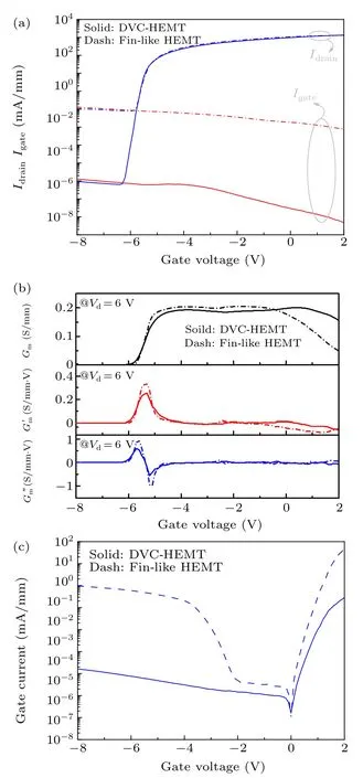
Fig.3. Comparison of(a)transfer characteristics(log),(b)transconductance(Gm)and high order transconductance( and ),and(c)Schottky characteristics between Fin-like HEMT and DVC-HEMT.
In addition to the improved DC characteristics, the current collapse (CC) of HEMT, severely limits the maximum output powers and deteriorates the device linearity, thus, the CC of DVC-HEMT was also calculated by the pulsed measurement. The pulsed measurements were performed by using the pulse of 500 ns in width and 1 ms in period(as shown in Fig. 4) to investigate the current dispersion of the device. At the bias point(VGSQ,VDSQ)=(−8 V,0 V),there is a potential difference between gate and drain,so the electrons in the gate electrode could be captured by the trap state. Therefore, the bias point(VGSQ,VDSQ)=(−8 V,0 V)is selected to evaluate the trap state and avoid the self-heating effect. Figure 4 shows that an 8.8% drain current (Id) reduction of Fin-like HEMT(as shown in Fig.4(b))happens atVGS=2 V andVDS=10 V while that of the DVC-HEMT(as shown in Fig.4(a))reduces by 3.2% at the same bias condition. Furthermore, the CC of DVC-HEMT is 5.0%at(VGSQ,VDSQ)=(8 V,20 V)while that of Fin-like HEMT is 11.2% at (VGSQ,VDSQ)=(8 V, 20 V),The results indicate that the N2O plasma pre-treatment can essentially suppress the trap state-related carrier trapping and thus contribute to the RF efficiency.[30]
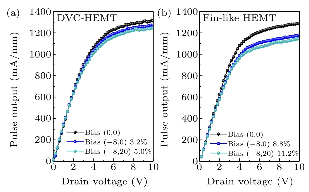
Fig. 4. Double-pulse characteristics of (a) DVC-HEMT and (b) Fin-like HEMT.
As shown in Fig.5(a),the maximum current–gain cutoff frequency(fT)and the maximum power gain cutoff frequency(fmax) of the DVC-HEMT are 40 GHz and 60 GHz, respectively. Due to increased gate-to-channel separation and lowerGmpeak for DVC-HEMT, the peakfTandfmaxare slightly lower than those of Fin-like HEMT.However,as demonstrated in Fig.5(b),fTandfmaxyield a flatter curve over a wider range of gate bias,which is associated with the increasedGmflatness of DVC-HEMT. Based on good agreement between theGmand small signal profile, we conclude that the modulation ofGmcharacteristics is advantages to improvefT/fmaxlinearity of DVC-HEMT compared to Fin-like HEMT.
To corroborate the device power characteristics and their effect on the millimeter-wave application performance,power measurement of HEMT at 30 GHz was performed in continuous wave using an on-wafer load pull system.The load and the source impendence were tuned for the optimum PAE, so that the power linear gain was lower than the small signal gain.Figures 6(a)and 6(b)illustrate the output power density(Pout),the power gain (Gain), and the PAE as a function of the input power (Pin) for the DVC-HEMT and Fin-like HEMT, respectively, both of which are characterized at deep-class AB operation atVd=20 V. Due to the excellent pinch-off characteristics, minimized gate current and suppressed CC,aPoutof 5.3 W/mm and a peak PAE of 41% are notably observed from Fig.6(a),whereas,those of Fin-like HEMT as shown in Fig.6(b)are 4 W/mm and 34%,respectively.Furthermore,the DVC-HEMT device exhibits a more flattened gain curve with the compression between the linear gain and associated gain is as low as 0.8 dB,as well as,for Fin-like HEMT,the gain compression is up to 2.7 dB.Due to the improvement of gain compression, aP1dBof 28 dBm is obtained by the DVC-HEMT,in contrast, Fin-like HEMT shows aP1dBof 25.2 dBm, indicating the smaller distortion of RF linearity in DVC-HEMT.The improvement of RF linearity performance is mainly attributed to the flatterGmprofile,which indicates that the proposed architecture has an obvious potentiality in the high linearity millimeter-wave application.
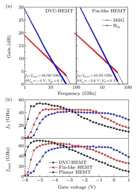
Fig.5. (a)Small signal characteristics of DVC-HEMT and Fin-like HEMT.(b) Gate voltage dependence of fT and fmax for DVC-HEMT, Fin-like HEMT,and planar HEMT at Vd=6 V.
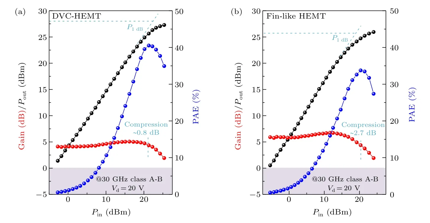
Fig.6. Comparison of output power characteristics after a load-pull at frequency of 30 GHz and Vd=20 V:(a)DVC-HEMT and(b)Fin-like HEMT.
4. Conclusion
This work presents a novel device namely DVC-HEMT obtained by integrating differentVthvalues including the slant recess element and planar element in parallel along the gate width with N2O plasma treatment on the gate region, to produce a device with high linearity performance in millimeterwave application. The fabricated DVC-HEMT exhibits a steadyGmandfT/fmaxplate curve with GVS of 7 V and a constantfT/fmaxof 40 GHz/60 GHz. Furtherly, it also features an exceptional linearity performance withP1dBof 28 dBm at frequency=30 GHz,Vd=20 V whereas that of the Fin-like HEMT is 25.2 dBm at same bias condition. The proposed architecture has an obvious potentiality in millimeter-wave application requiring good linearity and high efficiency.
Acknowledgments
Project supported by the National Key Research and Development Program of China(Grant No.2020YFB1804902),the Fundamental Research Funds for the Central Universities,the Innovation Fund of Xidian University,the National Natural Science Foundation of China(Grant No.61904135),the China Postdoctoral Science Foundation (Grant Nos. 2018M640957 and BX20200262), and the Research and Development Plan of Key Fields in Guangzhou(Grant No.202103020002).
猜你喜欢
吉林畜牧兽医(2022年9期)2022-09-19
今日农业(2022年13期)2022-09-15
今日农业(2021年9期)2021-11-26
今日农业(2021年14期)2021-10-14
当代陕西(2020年14期)2021-01-08
今日农业(2020年18期)2020-12-14
今日农业(2020年19期)2020-12-14
今日农业(2020年19期)2020-11-06
当代陕西(2019年12期)2019-07-12
今日农业(2019年13期)2019-01-03
- Chinese Physics B的其它文章
- High sensitivity plasmonic temperature sensor based on a side-polished photonic crystal fiber
- Digital synthesis of programmable photonic integrated circuits
- Non-Rayleigh photon statistics of superbunching pseudothermal light
- Refractive index sensing of double Fano resonance excited by nano-cube array coupled with multilayer all-dielectric film
- A novel polarization converter based on the band-stop frequency selective surface
- Effects of pulse energy ratios on plasma characteristics of dual-pulse fiber-optic laser-induced breakdown spectroscopy