
Differential nonlinear photocarrier radiometry for characterizing ultra-low energy boron implantation in silicon
2022-03-12 07:45XiaoKeLei雷晓轲BinChengLi李斌成QiMingSun孙启明JingWang王静ChunMingGao高椿明andYaFeiWang王亚非
Chinese Physics B 2022年3期
Xiao-Ke Lei(雷晓轲), Bin-Cheng Li(李斌成), Qi-Ming Sun(孙启明),Jing Wang(王静), Chun-Ming Gao(高椿明), and Ya-Fei Wang(王亚非)
School of Optoelectronic Science and Engineering,University of Electronic Science and Technology of China,Chengdu 610054,China
Keywords: ultra-low energy ion implantation, differential nonlinear photocarrier radiometry, junction depth,electronic transport parameters
1. Introduction
As the fabrication of silicon CMOS devices develops toward the nanotechnology,the ultra-shallow source/drain(S/D)junction acting as an essential part of silicon CMOS devices is required to meet the requirements, specifically specking,abruptly steep doping profile and highly active doping concentration, further, both of which are confined within the top nanometers of substrate.[1,2]The processing and characterization of shallow junctions consequently face extreme challenges.[3,4]The technological process, usually adopted such a treatment as combining ultra-low energy ion implantation with rapid-thermal annealing treatment to achieve a well reliable reproducibility and the good control of implanted atoms,dosage and spatial distributions,is extensively used to form shallow junctions of ultra-shallow source/drain junctions(USJ)wafers.[5-7]The ion implantation with the precise control of junction depth and doping concentration is closely related to the scaling of source/drain(S/D)junctions.[1,8]Scaled junction processing should simultaneously accomplish two objectives: limiting the diffusion of impurities to maintain the thermal budget, and substantially activating the implantation atoms. For the boron implanted ultra-shallow junctions studied in this paper,it means that the group III acceptor B atoms should be placed on the lattice or substitution site in silicon target.The measurement techniques of electronic properties of ultra-shallow junctions continuously develop to keep up with the scaling of devices. The shallow junction characteristics depend strongly on implantation conditions such as species,energy, dose, and temperature, and the relevant ultra-low energy implantation techniques and processing conditions.[9,10]In the meantime,shallow junction characteristics also depend strongly on thermal annealing techniques.[11]The distribution of depth at which the ions eventually reside in silicon,the lattice damage induced by the ions and high energy recoils,and the relocation of doping atoms by diffusion during thermal annealing are all essential quantities in junction processing.[12,13]It is necessary to quantitatively analyze the formation and dissolution of defects in shallow junctions by analyzing the depth distribution of implanted atoms in silicon and the electronic parameters characterizing the electrical activity. Therefore,the real-time monitoring and precise controlling of processing parameters and the accurate evaluating the recrystallization and impurity activation are critical to the achievement of the device miniaturization and the control of demanded damage well during the ultra-shallow junction processing.[14]The real-time inspection analysis is one of the key steps for determining the final quality and structure of USJ during processing.
In this paper, the differential nonlinear photocarrier radiometry(PCR)measurement is performed to investigate and characterize the electrical activity and junction depth for different ultra-low-energy ion implantations in silicon. Experimentally, four USJ samples with implantation energy of 0.5 keV, 1 keV, 2.5 keV, and 5 keV and one reference sample are measured by using PCR frequency scan(dependences of PCR amplitude and phase on modulation frequency)under 405-nm excitation at 44.5 mW.The raw PCR signal measured from the reference sample is utilized to normalize that from the implanted surface of the USJ wafers to obtain the differential amplitude and phase data which eliminate the instrumental frequency response(IFR)completely. The parameters of shallow junction are extracted via a multi-parameter estimation procedure. The correlation between differential PCR signal and implantation energy is explained by the effect of the implantation energy on the electronic properties and junction thickness of USJ wafers in detail. In addition,the depth profiles of boron atoms in silicon substrate under four different ultra-low implantation energy values are calculated by the SRIM program, and thus the thickness values of shallow junction with an electrical damage threshold (YED) of 5.3×1015cm-3are determined. The junction depth values determined by the two techniques are analyzed and discussed for the USJ wafers.
2. Material and experiment
2.1. Material process and SRIM measurement
Four USJ wafers under test are selected from a batch of 100-oriented N-type c-Si samples, are implanted with boron ion under ultra-low energy.Compared with the heavy ions,the implanted boron ions transfer less energy to the target atoms and have a large scattering angle, thereby contributing to a small number of displaced atoms in silicon target. The movement direction of boron ions changes greatly, and the shallow layer has a large-damaged region with the serrated shape and the high non-overlapping damage density. A subsequent thermal annealing treatment for 1 s at a peak temperature of 1050°C is absolutely necessary to highly activate the dopants into effective electronic impurities and eliminate most of the surface lattice damages caused by low-energy ion implantation in silicon wafer, implying that the lifetime and mobility of minority carriers of shallow junction are recovered and its optical properties in visible and near infrared ranges are close to those of the crystalline silicon.[4]The implanted surfaces are all chemo-mechanically polished. The specimen processing conditions are summarized in Table 1. In addition,a nonimplanted and non-annealed (NINA) wafer are also prepared to be used as the reference sample for the differential measurement.

Table 1. Processing parameters of USJ wafers under test.
The stoppings and ranges of implanted impurities in silicon wafers with the different processing parameters such as implantation species, implantation energy,etc. are determined by a comprehensive SRIM program based on the Monte Carlo method resulting from its reliability and wide acceptance as an industry standard in modeling the ion trajectories in solid.[15-17]We carefully study the ion-implantationinduced shallow region on the upper surface of silicon wafer at different ultra-low implantation energy values. The typical impurity depth profile as shown in Fig. 1 highlights the boron atom density along the depth direction in silicon substrate. There is a notable feature for the ion depth profiles of the heavily doped silicon wafers with the fixed implantation dose: the bombarded B+atoms gradually penetrate into the silicon target, contributing to the ion depth profile expansion and reducing its peak with the implantation energy increasing. The peaks of depth profiles are located at 5.6 nm,7.7 nm,13.6 nm,and 23.1 nm for the implantation energies of 0.5 keV,1 keV,2.5 keV,and 5 keV,respectively.
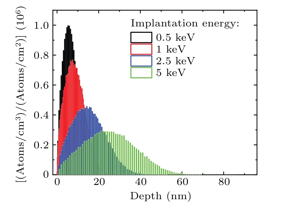
Fig.1. Typical ion depth profiles of boron-implanted USJ wafer at ultra-low implantation energy ranging from 0.5 keV to 5 keV.
The B+atom concentration distributions with various implantation energy values are derived by multiplying the depth profile shown in Fig.1 by the implantation dose 1×1015cm-2and are shown in Fig.2.The basic definition of electrical damage threshold(YED)is used to significantly simplify the corresponding correlation between the degree of lattice damage of the implanted layer in silicon and its electrical properties by avoiding the use of the complicated theoretical model.[18]The implanted layer is generally composed of the region traversed by the implanted atoms and the region in which the atoms eventually reside,and its thickness is generally defined as the distance between the wafer surface and the internal intersection between the electrical damage threshold and the impurity concentration depth profile due to the much higher sensitivity of electronic properties to the activation degree of implanted atoms and crystalline damage as the much higher sensitivity of electronic properties to the activation degree of implanted atoms and crystalline damage.[19,20]According to the calculated electrical damage threshold(YED)of the boron-implanted silicon wafer with aYEDof 5.3×1015cm-3,[21,22]the determined thickness values of the shallow junction are listed in Table 1. The results indicate that the lower the implantation energy,the shallower the formed junction is.
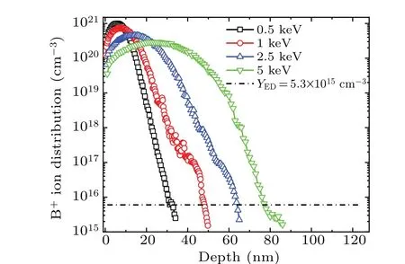
Fig.2. Depth-dependent implanted boron concentrations with four different implantation values at high implantation dose of 1×1015 cm-2.
2.2. Differential nonlinear PCR measurements
Room-temperature frequency-scanning measurements are conducted with a PCR measurement system. Wafers are excited via a 405-nm semiconductor laser with an output power of around 45 mW monitored by a power meter. The laser is periodically modulated by a function generator and then focuses onto the sample surface by a focusing lens. The small focus spot is employed due to the power output limitation of laser to obtain the PCR signal with enough high signal-to-noise ratio (SNR). The radius of beam tightly focused onto the sample surface, measured by a knife-edge approach, is approximately 35 μm. The periodic PCR signals are collected through a pair of off-axis paraboloidal mirrors and detected by an InGaAs photodetector whose spectral range of response spans from 700 nm to 1800 nm and the effective detection radius is approximately 55 μm,and then are demodulated by a lock-in amplifier and thus the resulting amplitude and phase data are outputted. The absorption coefficient of the crystalline silicon (c-Si) at 405-nm wavelength is set to be 1.02×10⁷m-1, and the corresponding optical penetration depth is approximately 0.098 μm.[23]To investigate the effect of implantation energy on electronic properties and junction depth of USJ wafers,we perform the PCR frequency-scanning measurements for four different USJ wafers. An NINA wafer is used as the reference sample for the differential measurement.
When the silicon wafers with different processing parameters(implantation dose,implantation energy,annealing temperature,etc.) are investigated,[24,25]it is conventionally assumed that the transport properties of the substrate layer of all implanted samples are the same as those of the reference sample from the same batch.In this work,the transport parameters of the substrate layers are obtained by fitting the frequencydependent PCR amplitude and phase measured from the reference sample to a single-layer nonlinear PCR model,and the corresponding fitted values of the carrier lifetimeτand the carrier diffusion coefficientDare 589.3 μs and 16.5 cm2/s,respectively. The scaling of the electrical properties and thickness value of the shallow junction in silicon is based on their correlation to the activation degree of implanted atoms and damage to the lattice in the ion implantation and thermally annealing process. In the fitting process, the electronic transport parameters of the boron-implanted shallow junction,i.e.,the minority carrier lifetimeτ1,the carrier diffusion coefficientD1, and the front surface recombination velocitys1as well as the thicknessL1of the shallow junction are set to be free variables. In addition, the rear surface recombination velocitys2is assumed to be 100 m/s.[26]Considering the influence of vignetting and defocusing,the effective detection radius of photodetector obtained by fitting the PCR data of the reference sample to the corresponding theoretical mode is used instead of the real radius (500 μm) which is much larger than the former.[27]
3. Results and discussion
The experimental differential PCR amplitude and phase data as well as the corresponding theoretical best fits are illustrated in Fig. 3 for all four boron-implanted USJ wafers.Good agreement between the experimental results and theoretical curves is obtained. As the implantation energy increases,the implantation damage is gradually aggravated and thus it is more difficult to recover in the annealing process. The thicker implantation layer and the higher electrical defect concentration hinder the radiation recombination and thus enhance the non-radiation recombination pathway. Therefore, the PCR amplitude and phase lag both decrease monotonically with the implantation energy increasing. This is mainly due to that the wider damage region with the implantation energy gives rise to the increase of its relative contribution weight in the total photogeneration unit.

Fig. 3. Modulation frequency-dependent differential PCR amplitudes (a)and phases (b) at 405-nm excitation for four boron-implanted USJ wafers with different implantation energy values,with NINA wafer acting as a reference sample, and symbols and solid lines representing experimental data and the corresponding best fits,respectively.
Figure 3 shows that the frequency behavior of the differential PCR signal can be broken into three regions in the entire energy range studied. The differential amplitudes are approximately 1 at the low frequency end that exhibits independent behavior of the modulation frequency as shown in Fig. 3(a).As the frequency increases to higher than 1 kHz, the amplitude values decrease rapidly and come to minimum values at a frequency range of ca. 60 kHz-110 kHz, and then start to increase at higher frequencies. Similarly, the phase lags are approximately 0 at lower modulated frequencies and start to increase slightly at intermediate frequency end. However,the modulation frequency is higher than about 10 kHz, the opposite monotonic behavior of phase lag appears. From this figure, it is evident that as the implantation energy increases,the position corresponding with the minimum amplitude value moves toward the low frequencies.
It is noted from Fig.3 that the energy dependence of PCR signal exhibits an obvious monotonic characteristic within the medium and high frequency range.This is a result of the larger carrier-wave contribution weight generated in shallow junction in the overall PCR signal due to the shorter carrier-wave diffusion length at higher frequency. Experimentally it is found that,with thought for both PCR phase and amplitude,the most sensitive frequency range derived from these figures is about 10 kHz-220 kHz.
As is well known that the structural,electronic,and optical properties of the surface and sub-surface regions for silicon wafers are greatly affected by the ion implantation and thermal annealing processing. The effect of energy on PCR amplitude and phase lag can be explained through the electronic transport characteristics and depth value of the shallow junction varying monotonically with the implantation energy. The differential nonlinear PCR model is utilized in the multi-parameter fitting. In Table 3 are summarized the best-fitted results and mean square variances extracted from the best-fitting procedures presented in Fig.3. The electronic parameters related to the carrier density wave such as minority carrier lifetimeτ1,carrier diffusion coefficientD1of the boron-implanted shallow junctions with four different implantation energy values are much lower than those of the substrate wafers. In addition,it is observed that the minority carrier lifetimeτ1and carrier diffusion coefficientD1are significantly sensitive to the degree of electrical activation of implanted atoms and damage to the lattice structure,and exhibit a monotonic variation with the implantation energy.
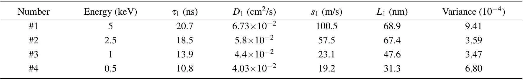
Table 2. Determined electronic properties and thickness values for four different USJ wafers obtained by the differential nonlinear PCR technique.
Figure 4 presents the determined electronic parameters and thickness of the shallow junction in silicon as a function of the implantation energy under the NINA reference sample.The determined results clearly show that electronic parametersτ1,D1,s1, and the thicknessL1of the shallow junction in silicon increase monotonically with the implantation energy increasing. For a given high implantation dose, the decreasing of the minority carrier lifetimeτ1with the increasing of impurity density is due to the fact that the depth profile of implanted atoms becomes narrower and its peak value increases with the implantation energy decreasing.[28,29]Simultaneously,the higher impurity density within the shallow junction increases the probability of carrier scattering,contributing to the decrease of carrier diffusion coefficientD1. No firm explanation has been put forward for the increase ofs1with the implantation energy in the literature. One explanation is that the built-in electrical field generated near the junction depth after the ion implantation and thermal annealing process limits the diffusion behavior of excess carrier to the material surface,and thus reducing the surface recombination velocitys1.[30]The alternative explanation is that the dislocation loops generated around the junction depth after the ion implantation and thermal annealing process confine the excess carrier spatially through the local strain field and then lower the non-radiation recombination of carriers on the sample surface, thereby resulting in the decrease ofs1.[31-33]
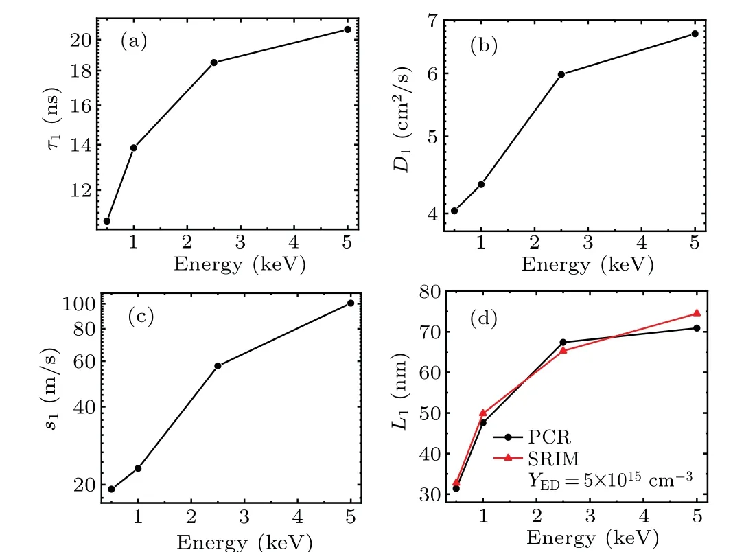
Fig.4. Curves of extracted electronic transport parameters and thickness of boron-implanted layer versus implantation energy,respectively,showing(a)minority carrier lifetime τ1 versus energy, (b) carrier diffusion coefficient D1 versus energy,(c)front surface recombination velocity s1 versus energy,and(d)thickness of boron-implanted layer L1 versus energy.
It is intriguing to notice that the thickness (L1) values of the shallow junctions in silicon determined by PCR technique at the different implantation energy values are generally in agreement with those calculated by SRIM program under the electrical damage thresholdYED=5.3×1015cm-3.Smaller deviations are probably attributed to the fact that the SRIM simulation may not completely reflect the complexity of lattice structure for the boron-implanted and annealing USJ wafers under test. The above results show that the PCR techniques can not only accurately determine the junction depth values which are equivalent to those calculated by SRIM program, but also quantitatively characterize the performance of ultra-shallow junction wafers by extracting the electronic parameters of the implanted layer.
A number of studies have been devoted to the characterizing of USJ wafers with various processing parameters in the past few years.[4,25]Huang and Ren[4]have employed the energy dependence of PCR signal at single frequency in combination with infrared spectroscopic ellipsometry(IRSE)data to investigate the junction depth and monitor the implantation energy for USJ wafers,and extracted the electronic properties of shallow junction to explain the dependence of PCR signal on energy. The corresponding theoretical model of PCR measurement is based on the linear proportion between the luminescence intensity and photogenerated carrier density. While the existing nonlinearity issue of PCR technique may affect the consistency between the above theory reliability and experimental measurement, the subsequent theoretical perfection is indispensable.[34,35]In addition,only PCR amplitude data are used in the fitting process.
To solve the above problems,the n-p product model,[36]which predicts that the band-to-band photoluminescence intensity is proportional to the product of the majority and minority carrier densities,is introduced to improve the model of USJ wafers in the PCR measurement. This work puts emphasis on the differential PCR measurements of shallow junction in the frequency domain to identify the most sensitive frequency range of PCR signal to energy,and thus achieving the optimal monitoring of energy. The frequency-dependent PCR amplitude and phase are fitted simultaneously to the differential nonlinear theoretical model in the multiparameter fitting,which is expected to obtain more accurate electronic information from silicon wafers. The lower implantation energy results in a higher impurity density within the shallow junction under the fixed high implantation dose, which gives rise to the monotonic decreasing of the electronic properties involving transport parameters and depth of junction with the decreasing of energy as presented in Fig. 4. This monotonic trend of determined parameters well explains the behavior of PCR signal varying with energy,mapping the recovery behavior of structure damage induced by ion implantation and the electrical activation behavior of dopant boron.
In addition, the SRIM program is used to calculate the depth profiles of the implanted impurity in order to investigate the dependence of junction depth on implantation energy and the contribution of shallow junction to the total signal,thereby validating the results determined by the differential PCR technique.The above results show that the nonlinear PCR theory is applicable not only to explaining accurately the effects of implantation energy on the frequency behavior of the PCR signal but also to more fully extracting the electrical parameters and junction depth.
4. Conclusion and perspectives
Experimental measurements have demonstrated that SRIM and PCR are sensitive techniques for characterizing the ultra-lowenergy ion implantation in silicon. The monitoring of nm-level thickness and electronic properties of ultrashallow junctions exhibits apparent monotonicity over the industrially relevant energy range. The determined parameters well explain the dependence of PCR signal on implantation energy and further quantitatively characterize the recovery degrees of structure damage induced by ion implantation and the electrical activation degree of impurities. The depth profiles and depth values with an electrical damage threshold(YED)of 5.3×1015cm-3are also calculated by the SRIM simultaneously,and the determined thickness values fit well with those extracted by the differential PCR.The effectiveness of the experimental differential PCR technique and the corresponding theoretical model is not limited to the accurate characterization of the junction depth dependence on implantation energy nor to the evaluation of the effect of energy on its electrical activity involving the excess carrier diffusion,recombination behavior,and the nonlinear correlation between excitation power and PCR signals.In conclusion,the differential nonlinear PCR technique, which is improved by greatly shortening the measurement time through the simplification of reference sample,reflects the complexity of implantation silicon to be more realistic than the SRIM.It offers a potential application prospect for the near-line and in-line control and evaluation of the industrial semiconductor processes in the design and fabrication of silicon-based USJ devices.
Acknowledgement
Project supported by the National Natural Science Foundation of China (Grant Nos. 61771103, 61704023, and 61601092).
猜你喜欢
Chinese Physics B(2022年10期)2022-10-26
国际眼科杂志(2022年7期)2022-07-13
客联(2021年9期)2021-11-07
考试与评价·高二版(2021年2期)2021-09-10
考试与评价·七年级版(2020年6期)2020-11-02
考试与评价·七年级版(2020年5期)2020-10-29
考试与评价·七年级版(2020年4期)2020-10-23
青年生活(2019年16期)2019-10-21
商情(2017年17期)2017-06-10
幼儿智力世界(2006年2期)2006-03-08

- Chinese Physics B的其它文章
- Measurements of the 107Ag neutron capture cross sections with pulse height weighting technique at the CSNS Back-n facility
- Measuring Loschmidt echo via Floquet engineering in superconducting circuits
- Electronic structure and spin-orbit coupling in ternary transition metal chalcogenides Cu2TlX2(X =Se,Te)
- Characterization of the N-polar GaN film grown on C-plane sapphire and misoriented C-plane sapphire substrates by MOCVD
- Review on typical applications and computational optimizations based on semiclassical methods in strong-field physics
- Quantum partial least squares regression algorithm for multiple correlation problem