
Exciton luminescence and many-body effect of monolayer WS2 at room temperature
2022-05-16 07:12JianMinWu吴建民LiHuiLi黎立辉WeiHaoZheng郑玮豪BiYuanZheng郑弼元ZheYuanXu徐哲元XueHongZhang张学红ChenGuangZhu朱晨光KunWu吴琨ChiZhang张弛YingJiang蒋英XiaoLiZhu朱小莉andXiuJuanZhuang庄秀娟
Chinese Physics B 2022年5期
关键词:蒋英
Jian-Min Wu(吴建民) Li-Hui Li(黎立辉) Wei-Hao Zheng(郑玮豪) Bi-Yuan Zheng(郑弼元) Zhe-Yuan Xu(徐哲元)Xue-Hong Zhang(张学红) Chen-Guang Zhu(朱晨光) Kun Wu(吴琨) Chi Zhang(张弛) Ying Jiang(蒋英)Xiao-Li Zhu(朱小莉) and Xiu-Juan Zhuang(庄秀娟)
1Key Laboratory for Micro-Nano Physics and Technology of Hunan Province,School of Physics and Electronics,Hunan University,Changsha 410082,China
2College of Materials Science and Engineering,Hunan University,Changsha 410082,China
Keywords: transition metal dichalcogenides,photoluminescence,localized exciton,exciton density
1. Introduction
Transition metal dichalcogenides(TMDCs)with the formMX2(M=Mo,W andX=S,Se2,Te)have attracted attention due to their layer-dependent electronic structure. Owing to spatial confinement and weak dielectric screening,monolayer TMDCs exhibit a semiconducting direct-bandgap nature,[1,2]strong Coulomb interactions and high exciton binding energies that favor the formation of excitonic quasiparticles such as neutral excitons, charged excitons (trions), biexcitons and exciton–trion complexes.[3–9]The binding energies of these excitons are around hundreds of meV, making them stable even at room temperature.[10–12]In monolayer TMDCs, excitons (boson quasiparticles) are immersed in an environment of charged carriers and form a Fermi sea.[13]Therefore, monolayer TMDCs are an ideal system for exploring room-temperature many-body effects in two-dimensional systems.[14,15]
Owing to the excellent luminescence properties of TMDC excitons,photoluminescence(PL)has become the most commonly used experimental method to characterize and analyze the many-body effects.[13,14]In monolayer TMDCs, the existence of spin- and momentum-dark excitons, nonzero charge and spin degrees of freedom in charged excitons contribute to their luminescence properties for optical applications.[16–19]In addition, excitons interacting with defects lead to the formation of localized exciton states that strongly influence the PL spectra.[20,21]Radiated luminescence arises from the radiative recombination of excited states of carriers. Excitons dominate radiated luminescence in semiconductor-layered TMDC materials and are at the core of the luminescence process.[1,12,22,23]However, to the best of our knowledge, the evolution and interaction of excitons, exciton complexes and defects with increasing excitation power has not been well studied; hence,here we aim to understand these physical processes and their practical applications.
Using mechanically exfoliated monolayer WS2and PL spectroscopy, exciton emission peaks were confirmed through temperature-dependent and electric-field-tuned PL spectroscopy. We quantitatively analyzed the exciton concentration dependence on temperature as well as the concentration distribution of excitons at room temperature. The interaction regime between excitons,trions and localized excitons can be distinguished by three concentration ranges as the carrier concentration increases in the two-dimensional system. These ranges describe the existing exciton species and how the extinction density and exciton lifetime affect their concentration.
2. Exciton energy levels
The energy levels and emission diagrams of excitons,trions and biexcitons are shown in Fig.1. An exciton is a bound electron–hole pair, and the energy difference between its energy state and the conduction band minimum is the exciton binding energy, denoted asEbX. The exciton binding energies of TMDCs are typically hundreds of meV,orders of magnitude larger than those in quantum wells. Disorder caused by defects in monolayer TMDCs can have an impact on the physical behavior of excitons,resulting in spectral broadening and localization. We denote these localized exciton states as LX.[21,24]Combining a neutral exciton with one electron/hole or another exciton generates trions (X-or X+) or biexcitons(XX),respectively,
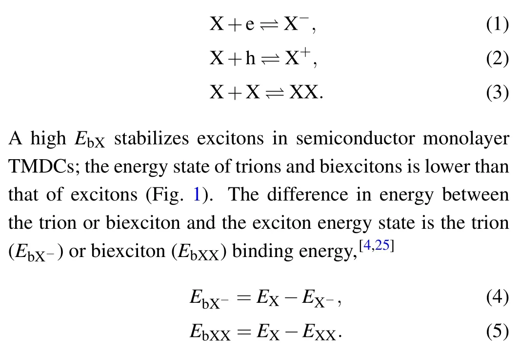
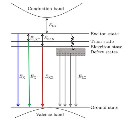
Fig. 1. Band structure and energy states of excitons, trions, biexcitons, and localized excitons of some monolayer TMDCs.
The above-mentioned excitons, trions and biexcitons are produced by the Coulomb interaction of multiple particles,especially when a strong light pulse hits a solid material. This phenomenon is termed the‘many-body effect’.[6,13,14]Studies on biexcitons are typically performed at low temperatures because they dissociate at room temperature.[6,26–28]As shown in the reverse reactions expressed by Eqs. (1)–(3), trions and biexcitons can be dissociated to neutral excitons when the system temperature is slightly high, sinceEbX-andEbXXare of the order of tens of meV.[4,12,25]In addition, a significant increase in the concentration of excitons in the system will promote the formation of trions and biexcitons.[29]When studying the room-temperature PL properties of TMDC materials,the many-body effect caused by the temperature and photogenerated carrier concentration will be more complicated. It is therefore necessary to provide a comprehensive and systematic overview of the effect of temperature and exciton concentration on the PL mechanism of TMDCs. In this work,monolayer WS2was selected as a representative TMDC to investigate the many-body effect at different temperatures and exciton concentrations. Monolayer WS2, like most singlelayer TMDCs, is dominated by negatively charged excitons(n-doped) due to chalcogen vacancies that are the dominant intrinsic defects and cause unsaturated electrons in the surrounding transition metal atoms to act as electron donors.
3. Experiments
3.1. Sample preparation and device fabrication
WS2samples mechanically exfoliated from a bulk crystal were transferred onto Si/SiO2(300 nm) wafers using adhesive tape. E-beam lithography (EBL) and metal thermal evaporation were employed to deposit Au/Cr electrodes(50 nm/10 nm)on the samples.
3.2. Characterization and measurements
Raman and steady-state PL spectral measurements were performed using a confocal microscope (WITec alpha300)with a continuous wave (CW) 532 nm laser and spot size of about 2 μm. A 50×objective lens was used for PL measurements and a liquid-N2-cooled stage was used to control the temperature. The incident laser power was obtained using a power meter (PM100D, ThorLabs). Time-resolved photoluminescence (TRPL) spectra were collected using a confocal microscope and Ti:sapphire laser pulses at 400 nm (80 MHz repetition frequency and 80 fs pulse width). Laser pulses were generated by an 800 nm laser from a mode-locked oscillator(Tsunami 3941-X1BB,Spectra-Physics)placed behind a beta barium borate crystal and focused onto the sample with a spot size of about 3 μm by an objective lens(50×,Zeiss,0.75 NA).The emitted signal was reflected by a silver mirror and collected into a streak camera(C10910,Hamamatsu).
4. Results and discussion
Figure 2(a)shows the optical micrograph of a WS2sample, where the bright area is multilayer WS2and the dark area outlined by the yellow dashed line is monolayer WS2.The monolayer was characterized by PL and Raman spectroscopies (supplementary Fig. S1). Steady-state PL spectroscopy was performed to characterize the exciton species at 20 K (Fig. 2(b)). Through multi-peak fitting, the spectrum was found to comprise four peaks with Gaussian lineshapes. The summation of the four peaks matched the experimental spectra,except for a slight deviation in the wavelength range(620–640 nm,supplementary Fig.S2). We attribute the peak centered at 595 nm, located at the highest energy level(2.079 eV),to the neutral excitons.[26,30,31]The peak centered at 605 nm is assigned to the charged exciton,with anEbX-of~35 meV,[4,26,32,33]because the energy level(2.044 eV)was lower than that of the neutral exciton. The peak centered at 611 nm had the lowest energy level(2.024 eV)and may be assigned to an exciton complex, such as biexcitons.[6,25,26]The origin of these peaks is consistent with previously reported values.[26,31,34]Finally, the broad peak centered at 612.5 nm was attributed to the localized exciton emissions (LX).[26,30]The assignment of PL peaks was confirmed by temperatureand excitation-power-dependent PL spectroscopy.[6,25,26,30,31]
To further investigate the exciton species corresponding to PL peaks, the excitation power density dependence of the steady-state PL spectrum was analyzed at 20 K. From Fig.2(c),the emission peak intensities of exciton emission and trion emission were linear with respect to the excitation power density,and had slopes of 0.88 and 0.89,respectively.[26]Ideally, the intensity of the biexciton emission can be described by a power-law relation,IXX∝P2, whereIXXis the PL intensity of the biexciton,Pis the excitation power density and the log–log plot has a slope of 2.0. However, the biexcitons in our study exhibited a slope of 1.16 due to the lack of equilibrium between the exciton states.[35]The PL intensity of localized exciton emissions exhibited a superlinear dependence onPwith a log–log slope of 1.74, which may be caused by localized exciton emissions involving defects and conduction bands.[36]The full width at half maximum (FWHM) of the PL peaks offers insights into the emission characteristics. The FWHMs of the exciton, trion and biexciton emissions were about 4 nm and not affected by the excitation power density,while the FWHM of localized exciton emissions decreased from 14 nm to 8 nm with increasing excitation power density (Fig. 2(d)), which may be explained by the superlinear relationship of localized exciton emissions. Typically, an excitation light source causes an observable thermal effect when a CW laser is used. However, we did not observe a distinct thermal effect in monolayer WS2, which may be due to its low light absorption rate.[2]From the power-dependent PL spectra at 20 K (supplementary Fig. S3), the characteristic peak positions and the shape of the curve for each excitonic species did not change for an excitation power density less than 258 W/cm2. This implies that there was no distinct thermal effect on our monolayer WS2from the CW laser, which may be due to the low light absorption rate of monolayer WS2.[37]Otherwise, the spectral features will change significantly(see the temperature-dependent PL spectra in Fig.3(a)).When the excitation power density exceeded 258 W/cm2,the exciton,trion,and biexciton peak positions redshifted by about 2 nm,which may be related to the bandgap renormalization induced by a high carrier concentration or a small thermal effect.

Fig. 2. (a) Optical micrograph of mechanical mechanically exfoliated monolayer WS2. (b) PL spectrum of monolayer WS2 at 20 K under an excitation power density of 512 W/cm2. The overall PL profile is black and fitted into four peaks,one each for excitons(X),trions(X-),biexcitons(XX)and localized excitons (LX). (c) Double-logarithmic plot of the integrated PL intensity of the exciton, trion, biexciton and localized exciton peaks as a function of the excitation density, and the corresponding linear fitting for their peak intensities. (d)FWHMs of excitons, trions, biexcitons and localized exciton emission peaks versus the excitation power density. The excitons,trions,biexcitons,and localized excitons are denoted in blue,green,red and gray,respectively.

Fig. 3. (a) Multi-peak simulation of normalized PL spectra for a series of temperatures under an excitation power of 255 W/cm2. The peak positions for exciton,trion,and biexciton emission are guided by corresponding lines. (b)Emission peak positions of excitons,trions,biexcitons,and localized excitons as a function of the temperature, and corresponding Varshni fitting. (c) FWHMs of exciton, trion, biexciton and localized exciton emission peaks versus temperature. The excitons,trions,biexcitons,and localized excitons are denoted in blue,green,red and gray,respectively.
Temperature-dependent PL spectra were acquired from 20 K to 295 K (Fig. 3(a)) to characterize the thermodynamic evolution of the exciton species in monolayer WS2. When the temperature was below 50 K,each PL spectrum consisted of four peaks (X, X-, XX, and LX), representing four distinct components at low temperatures. As the temperature increased,the biexciton peak vanished,which may be a result of biexciton dissociation induced by the thermal effect.When the temperature was between 60 K and 270 K,the PL spectra comprised three peaks(X,X-,and LX).The percentage by weight of the PL emission of excitons and trions increased with increasing temperature and decreased with increasing temperature for localized exciton emissions (supplementary Fig. S4).At temperatures above 270 K,the PL emission on the blue side was dominated by excitons and the broad PL emission on the red side could not distinguish between trion and localized exciton emissions. Therefore, the broad PL emission centered at 628 nm at room temperature is co-contributed by trion and localized exciton emissions (Fig. S5). The Varshni equation describes the temperature-dependent energy gaps corresponding to the exciton species,X,X-,and XX(Fig.3(b)),[26]

whereEg(0) is the band gap at 0 K, andαandβare phenomenological fit parameters. The curves of the exciton,trion and biexciton species were fitted;theEg(0)values were fitted to 2.082 eV,2.045 eV,and 2.030 eV,respectively(supplementary Table S1). From Eqs. (4) and (5),EbX-andEbXXwere calculated to be 35 meV and 55 meV, respectively, in agreement with previously reported values.[26]From the detailed multi-peak fit of the PL spectrum at 20 K in Fig. S2, the localized excitons have a series of corresponding defect states with an equal energy interval of 25 meV. Furthermore, four localized exciton emission peaks displayed a FWHM of about 7 nm,while P6 had a FWHM of about 4 nm.The temperaturedependent FWHM of the exciton and trion emission peaks increased from 2 nm to 8 nm and the FWHM of the localized exciton emissions increased from 10 nm to 24 nm(Fig.3(c)),which may be related to the presence of defects,and requires further study.
Room-temperature PL measurements were performed under different voltages to tune the intensities of the exciton and trion emission peaks.A schematic of the fabricated monolayer WS2device is shown in Fig. 4(a). The exfoliated monolayer WS2was transferred onto the Si wafer with 300 nm SiO2,and a voltage was applied across the electrode on the monolayer WS2and the silicon back. The PL spectra of the device varied with the gate voltage (Vg) under an excitation power density of 8.15 kW/cm2(Fig.4(b)). When a negativeVgwas applied,the exciton peak was dominant and the X-/LX peak was suppressed. When a positiveVgwas applied,the X peak was suppressed. Similar trends were observed when the sample was excited by power densities of 254.6 W/cm2and 2.36 kW/cm2(supplementary Fig. S6). This phenomenon is caused by the dependence of charged excitons (X-) on the applied electric field.[4]TRPL was utilized to understand the dynamics of exciton recombination. Figures 4(c)and 4(d)show the PL decay curves of X and X-/LX emission,respectively,under an excitation power density of 8.15 kW/cm2. A biexponential function was used to fit the PL lifetimes of X and X-/LX.[38]Both lifetimes increased as the voltage decreased,and reached their maximum values at aVgof-20 V. Under a negativeVg, the lifetime for exciton emission was longer than that of X-/LX.This may arise from electrostatic doping,which increases the exciton concentration and promotes the reverse reaction stated in Eq.(1).[4]
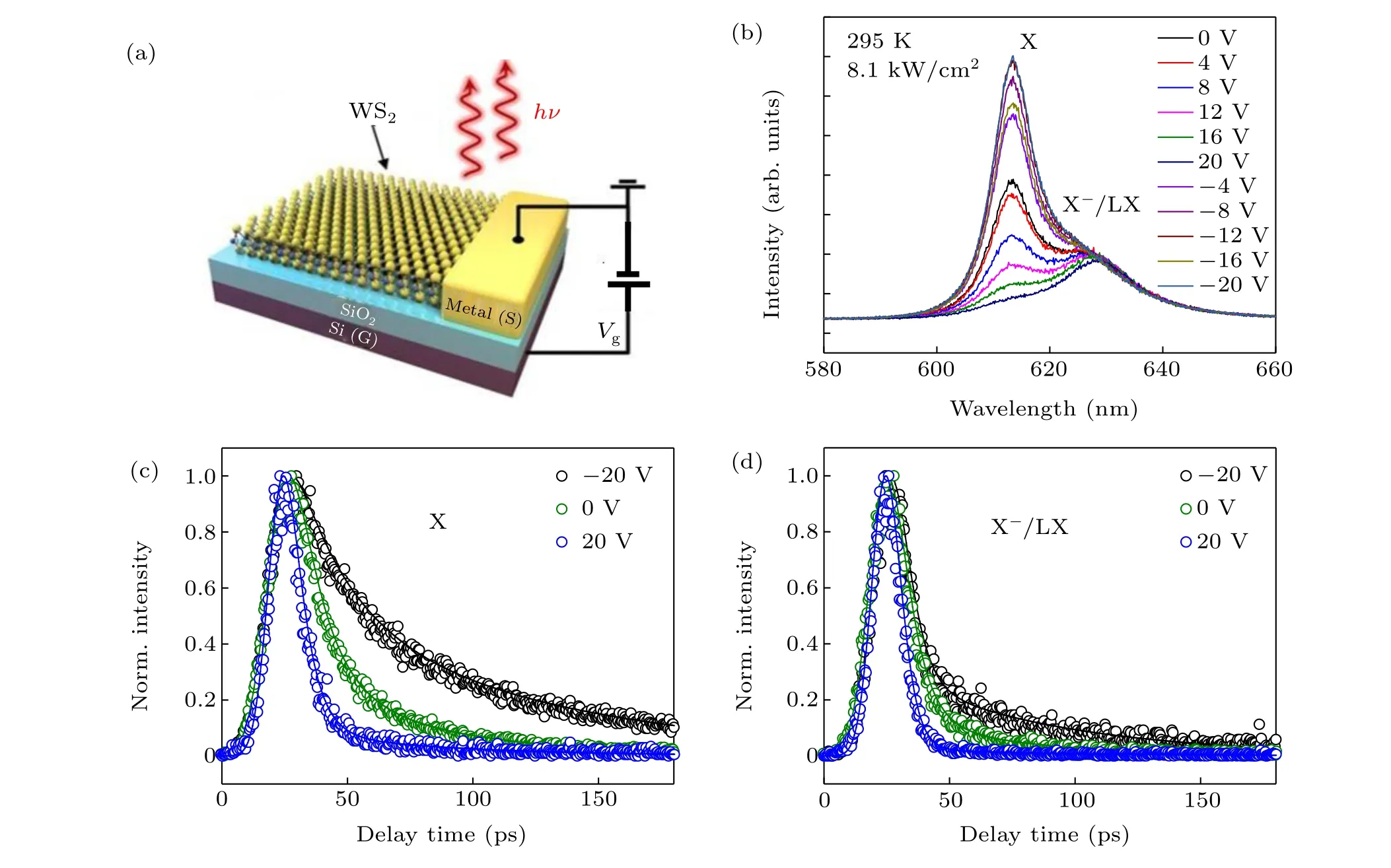
Fig.4. (a)Schematic of the fabricated devices. (b)PL spectra at 295 K for different gate voltages. (c)TRPL of X at different gate voltages and(d)TRPL of X-/LX at different gate voltages. Lines show the fitting functions.
The photogenerated carrier density is a key factor that affects the luminescence properties of materials. Therefore,we tuned the excitation light power density to obtain a nonlinear carrier density and investigated the effect of carrier concentration on the evolution of excitonic species in monolayer WS2at room temperature. Figure 5(a)shows the variation in the PL spectra with increasing excitation power density from 5.1 W/cm2to 32.6 kW/cm2. When the excitation power density was less than 127.3 W/cm2, the PL spectra exhibited a single peak feature centered at 620 nm, corresponding to the exciton emission.[39]When the excitation power density exceeded 127.3 W/cm2,another peak appeared at approximately 630 nm,corresponding to the overlapped emission of X-/LX.Furthermore,the percentage by weight of the X-/LX emission intensity increased with increasing excitation power density.As the excitation power density increased, the X-/LX peak position red-shifted, while the X peak position was retained(Fig. S7). When the excitation light power density reached 32.6 kW/cm2,the intensity of X-/LX was higher than that of X.Figure 5(b)presents a log–log plot of the excitation power density dependence of the X and X-/LX PL intensities. The plots can be divided into three linear regions.When the excitation power density is less than~1 W/cm2,the X intensity has a linear dependence on the excitation power intensity with a slope of 0.91(stage I).Within this stage,the intrinsic exciton recombination is dominant. When the excitation power density is between 1 W/cm2and 104W/cm2, the slope of the X intensity has a sublinear dependence and the slope decreases to 0.35 (stage II). Within this stage, the linear dependence of the X intensity decreases to sublinear, which can be ascribed to exciton–exciton annihilation in which the relaxation process is nonradiative recombination.[40–42]When the power density reaches 100 W/cm2, the X-/LX emission dominates the PL peak centered at 630 nm (TRPL data in Fig. 5(c)) and shows a sublinear dependence on the excitation power intensity with a slope of 0.52. When the excitation power density exceeds 104W/cm2, the intensity of X reaches a maximum and then decreases(stage III).Within this stage,the radiation recombination of the exciton reaches saturation. Excitons form trions and interact with defects to form the localized exciton more quickly; therefore, the X-/LX emission peak intensity maintains a sublinear slope. At stage I, the exciton concentration was between 2×106cm-2and 2×107cm-2, and the dominant species in monolayer WS2was the neutral exciton.When the exciton concentration was higher than~2×107cm-2, a significant concentration of trions appeared and the forward reaction in Eq.(3)commenced.At stage II,where exciton concentrations ranged from 2×107cm-2to 3×109cm-2,neutral and charged excitons coexisted and their concentrations were in equilibrium. As the exciton concentration increased further,the forward rate of the reaction in Eq. (3) dominated. As a result, trions become the dominant species in the system. At stage III,the exciton concentration ranged from 3×109cm-2to 2×1010cm-2and charged excitons become the dominant species in monolayer WS2,which may be accompanied by localized excitons(supplementary Table S3).
When the exciton concentration was high in stages II and III, exciton–exciton annihilation caused the exciton lifetime and quantum efficiency to decrease. The TRPL decay curves of X under a series of excitation power densities are displayed in Fig. 5(c). The lifetime decreased with increasing excitation power density(Table S2,Figs.S8(a)–S8(c)). This can be interpreted as the enhanced interaction between excitons and excitons,as well as excitons and defects,with increasing excitation power density. The TRPL of X-/LX under different excitation power densities is shown in Fig.S8(e).The lifetime of X-/LX decreased with increasing excitation power density. A schematic(Fig.5(d))shows the corresponding exciton species and their concentration distributions at three excitation power density ranges.
The exciton concentration can be obtained from

wherePis the excitation power,τis the exciton lifetime,hνis the energy of the excitation photon,Sis the spot area of the excitation light andηis the absorption efficiency. A CW laser with a wavelength of 532 nm and spot size of~2 μm was used.ηwas estimated to be 10%. The exciton concentration in the system is affected by the excitation power densityP/S,and exciton lifetimeτ. Moreover,the excitation power density and exciton lifetime affect one another. For example, when the excitation power density is increased, the concentration of photogenerated carriers also increases. However,when the exciton concentration is high, exciton–exciton annihilation is strong. Exciton–exciton annihilation shortens the exciton lifetime,which further reduces the steady-state exciton concentration. Therefore, the exciton concentration saturates when the excitation power density increases to a relatively high value(Fig.5(b)).
Fig.5. (a)Normalized PL spectrum of monolayer WS2 at room temperature with different excitation powers. The overall PL profile is black and fitted into two peaks,X(blue area)and X-/LX(gray area). (b)Double-logarithmic excitation power density dependence on the X(blue dots)and X-/LX(gray dots)emission intensities. (c)TRPL of X.Lines show the fitting functions. (d)Schematic of exciton density. X-/LX starts to appear at stage II.
5. Conclusion
Based on systematic analysis of temperature-dependent and excitation power density-dependent PL spectra, we investigated the many-body effect in mechanically exfoliated monolayer WS2at room temperature. From the temperaturedependent PL spectra,we found that the system is dominated by excitons for low-power excitation at room temperature. A small fraction of trions and the defect emission spectra overlap to form a band tail at the low-energy side of the PL spectrum. The exciton binding energies of trions were determined to be 35 meV.Tuning the room-temperature excitation power density in monolayer WS2from 22 mW/cm2to 32.6 kW/cm2resulted in a broad exciton concentration distribution ranging from 106cm-2to 1010cm-2. The existence of exciton species in this concentration distribution can be divided into the range dominated by excitons, the coexistence range with trions, and the range where excitons are suppressed and trions dominate. Under a high excitation power density at room temperature, the localized exciton emission from defects coincided with the emission peak position of trions and resulted in broad spectral characteristics. Our study provides a semiquantitative description of the many-body effect of monolayer WS2at room temperature and provides a physical description for studying room-temperature optical properties and optoelectronic devices based on TMDC materials.Acknowledgment
Project supported by the National Natural Science Foundation of China (Grant Nos. 61635001, 52072117, and 51972105).
猜你喜欢
同舟共进(2021年8期)2021-08-30
启迪与智慧·上旬刊(2019年11期)2019-09-10
老年博览·上半月(2019年9期)2019-09-10
文萃报·周五版(2019年39期)2019-09-10
百家讲坛(2019年12期)2019-07-14
东方女性(2017年3期)2017-03-24
现代妇女(2014年5期)2014-09-10
恋爱婚姻家庭·养生版(2013年1期)2013-02-27
中国报道(2012年3期)2012-01-19
决策与信息(2010年3期)2010-09-20

- Chinese Physics B的其它文章
- A nonlocal Boussinesq equation: Multiple-soliton solutions and symmetry analysis
- Correlation and trust mechanism-based rumor propagation model in complex social networks
- Gauss quadrature based finite temperature Lanczos method
- Experimental realization of quantum controlled teleportation of arbitrary two-qubit state via a five-qubit entangled state
- Self-error-rejecting multipartite entanglement purification for electron systems assisted by quantum-dot spins in optical microcavities
- Pseudospin symmetric solutions of the Dirac equation with the modified Rosen–Morse potential using Nikiforov–Uvarov method and supersymmetric quantum mechanics approach