
Quantum key distribution transmitter chip based on hybrid-integration of silica and lithium niobates
2022-06-29 09:18XiaoLi李骁LiangLiangWang王亮亮JiashunZhang张家顺WeiChen陈巍YueWang王玥DanWu吴丹andJunMingAn安俊明
Chinese Physics B 2022年6期
关键词:张家
Xiao Li(李骁) Liang-Liang Wang(王亮亮) Jia-shun Zhang(张家顺) Wei Chen(陈巍)Yue Wang(王玥) Dan Wu(吴丹) and Jun-Ming An(安俊明)
1State Key Laboratory on Integrated Optoelectronics,Institute of Semiconductors,Chinese Academy of Sciences(CAS),Beijing 100083,China
2College of Materials Science and Opto-Electronic Technology,University of Chinese Academy of Sciences,Beijing 100049,China
3Center of Materials Science and Optoelectronics Engineering,University of Chinese Academy of Sciences,Beijing 100049,China
4CAS Key Laboratory of Quantum Information,University of Science and Technology of China,Hefei 230026,China
Keywords: quantum key distribution,hybrid-integration,BB84
1. Introduction
Cyber communication provides much convenience in daily life and becomes more and more indispensable to us.However the boost and innovation of computing capacity drastically increase the risk of failure for classic data encryption method. Therefore the need for higher-level information security becomes urgent. Quantum key distribution(QKD)can ensure best security based on quantum mechanics. Bennett and Brassard,[1]and Bennettet al.,[2]first proposed the effective and famous BB84 protocol. Bulk optics connected by fibers were used for the realization of BB84 protocol,in which weak coherent pulse pairs(WCPs)with a temporal delay were generated for encoding and decoding quantum states.[3,4]In these systems too much room,however,is required for apparatuses to lay on a heavy and large optical platform,which is not conducive to manufacture and practical applications.
One way to miniaturize the system is to turn into integrated photonics technology. Silica planar light-wave circuits(PLCs) have been used first for the WCP generation at Alice and state decoding at Bob.[5–14]Recently,various photonic integrated circuits (PICs) technologies have been integrated into QKD systems,such as indium phosphide(InP)[15,16]and Si photonic (SiP)[17–23]based integrated photonic platforms,which have shown a good application prospect.The BB84 system based on the combination of a silica asymmetric Mach–Zehnder interferometer(AMZI)and off-chip lithium niobates(LN)modulators was reported,[9,13]where high speed of phase modulation and intensity modulation were implemented by extra LN modulators.
To further increase the degree of integration,a promising way is to integrate silica and LN into one single chip. The relevant technology has been reported in the field of coherence communication,[24]where low-loss silica PLCs and LN phase modulator array chip were spliced together to implement quadrature phase shift keying (QPSK). In the field of QKD,Nambuet al. demonstrated a prototype of BB84 QKD transmitter based on hybrid integration,[25]where an AMZI silica PLC was coupled with an MZI LN PLC. His demo could realize the high-speed intensity modulation but lacked the function to modulate relative phase between WCPs in a dynamic fashion and a fast fashion.
Here we present a transmitter with a different structure based on this hybrid-integration technique. There are two main parts in our chip. One is the silica part which consists of a tunable directional coupler(DC)and 400-ps delay line. The other is the LN part which consists of a Y-branch,with electrooptic(EO)modulators on both arms. The two parts are facetcoupled to form an AMZI.Our design has three features.First,we make it in one single AMZI to implement both functions of WCP generation and high-speed relative phase modulation.This is different from other researches[9–14]where these two functions are usually done by separate apparatuses. Second,a combination of slow silica thermo-optic phase modulator(TOPM) and fast LN EO phase modulator makes our chip more flexible to regulate any defined relative phase. Third,the LN phase modulator is designed in a push-and-pull model in order to reach a higher EO modulation efficiency. With the aid of an extra off-chip LN intensity modulator and a passive silica decoder chip,[26]we demonstrate the preparation of four BB84 states and the corresponding states decoding.
2. Design and fabrication of hybrid chip
We design and fabricate a hybrid chip for a telecom(1.55 μm) wavelength window. The structure is shown in Fig.1(a). The silica chip on the left consists of two sub-parts.Part 1 is a 2×2 MZI with a TOPM1 in one arm,which functions as a tunable DC. Part 2 consist of two arms of waveguides,whose path difference produces 400-ps temporal delay.There is another TOPM2 in the short arm. It is worth noting that this silica part is different from that in Ref. [26], which is terminated with a DC at the output. We here remove the DC for the coupling with the LN chip. The relative refractive index differenceΔis 2.0% between the waveguide core and cladding. The full-vectorial beam propagation method(BPM)is used to find the geometric zero birefringence condition for the stripe waveguides, where the effective indices are found equal for both TE and TM modes. The fabrication process can be referred to Refs.[26,27].
The LN chip on the right has a Y-branch structure, with electro-optic (EO) modulators on both arms. The groundsignal-ground (GSG) coplanar waveguide electrodes are designed in a push-pull model,making electric fields opposite to each other for both arms. The LN modulation chip is prepared by diffusion method. First, the design waveguide structure pattern is transferred to the LN wafer by lithography. Next,the wafer is placed into the C6H5COOH solution at 120°C–250°C,where Li-in the lithium niobate material is exchanged with H+to form the core HxLi1-xNbO3and diffused for 5 h–10 h at 300°C–400°C to form the exchange diffusion waveguide. The relative refractive index differenceΔis about 0.3%between the waveguide core and cladding. Then photolithography is again used to transfer the traveling wave electrode pattern, and the GSG electrode is formed by electroplating method.
The silica chip is facet-coupled with a single mode fiber array (FA) on the left side, with a coupling loss of 0.4 dB.The LN chip is facet-coupled with a polarization maintenance FA on the right side,whose slow-axis coincides with thex-cut direction of LN chip, with a coupling loss of 3 dB. Next the silica and LN chips,with the connecting end-faces polished at an 8°angle, are facet-coupled to form an AMZI chip in the way shown in Fig. 1(a). The chip size is 2.3 cm×0.6 cm for silica part and 3.8 cm×0.1 cm for LN part. The hybrid chip is fixed on a large silicon substrate together with the designed printed circuit board(PCB).Wire bonding is employed to connect the electrodes between the PCB and the chip. The chip’s temperature is controlled by a commercial temperature controller(TEC)based on the Peltier effect.

Fig.1. (a)Schematic diagram of the hybrid-integration chip and(b)packaging.
3. Measurement of temporal delay and phase modulation speed
The temporal delay of the WCP generated by our hybrid chip is measured by both normal-intensity light and stronglyattenuated light(mean photon per cycleμ <0.01). A train of pulses, with pulse 50-ps duration, are input to our chip. The pulse pair graph in one cycle captured by the sampling oscilloscope(SOC)and the histogram of the two time-bins scanned by the gated-mode single photon detector(SPD)are shown in Figs.2(a)and 2(b),respectively.

Fig.2. Measurement of temporal delay of WCP for our chip: (a)measured by SOC with normal-intensity light, (b) measured by SPD with stronglyattenuated light(μ <0.01).
The measured temporal delay is 401.5 ps for SOC and 440 ps for SPD.The value for SPD is about 40 ps larger than that for SOC. This is because SPD has small time-resolution than SOC and its gate width is wider than 400 ps. Therefore the value of 401.5 measured by SOC is closer to the true one.The difference between measurement and design is below 0.4%,which proves the accuracy of our design and fabrication.
In addition,the speed of phase modulation for the hybrid chip is tested. The hybrid chip is fixed on the TEC platform and the microwave probe is used to connect GSG electrode on chip. As shown in Fig. 3, the eye diagram under 10 Gbps is obtained. The rise/fall time is around 100 ps and the extinction ratio of the eye diagram is 6.12 dB.From the test results,we can see that the modulation rate of the integrated chip can meet the needs of fast phase-encoding.

Fig.3.Eye diagram of hybrid chip.Green is driving signal from PPG before amplified;yellow is optical signal.
4. Polarization characteristic analysis on interference
In order to optimize the interference visibility in QKD,it is necessary to analyze the dependence of interference visibility on the chip temperature for both Alice and Bob chips.With the aid of the pulse self-interference method,[27]we conduct the following experiments. Considering the limit of our TEC,We scan the hybrid chip temperature from 17°C to 60°C.The interference fringes against temperature are shown in Fig.4(a).We can observe that the photon count for the TE mode is much larger than that of the TM mode. This is because the polarization characteristic of LN waveguide. Furthermore,the TE and TM modes are in phase despite the change of chip temperature. Since the visibility increases with the temperature and our TEC has lower control precision above 55°,we decide to use this value as the optimal temperature for the hybrid chip.Next, we use the same method to determine the Bob AMZI chip temperature as shown in Fig.4(b),In the vicinity of 42°,the visibility reaches a minimum value,and TE mode and TM mode are in anti-phase. Though in the scope of TEC temperature domain there is no such temperature point, where both modes are perfectly in phase, we obtain the best visibility as we can in the vicinity of 17°. Therefore the Bob chip temperature is set to be this value.
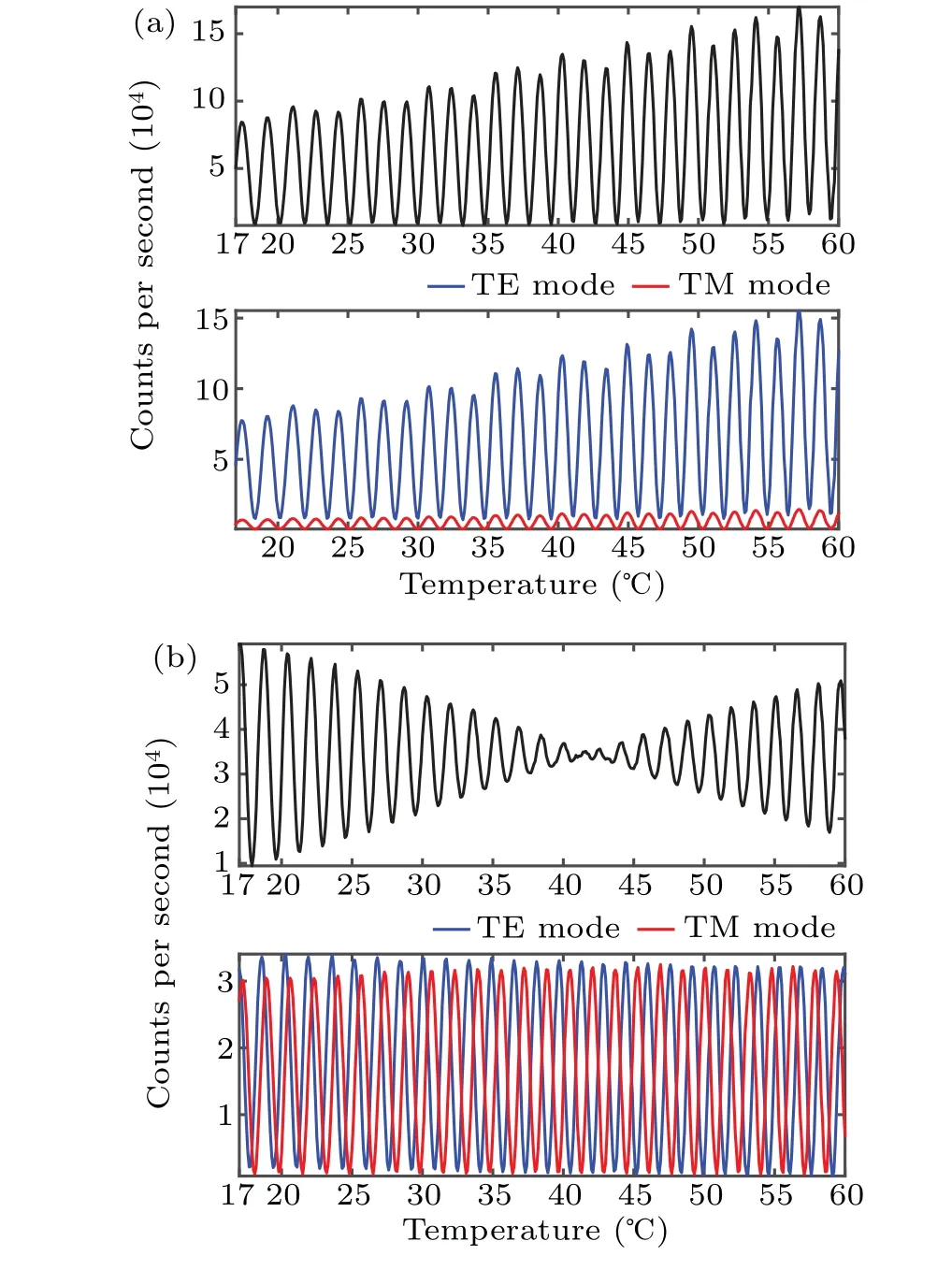
Fig. 4. Interference fringes of TE mode (blue) and TM mode (red) versus chip temperature in a range from 17 °C to 60 °C.Top black curve is the sum of TE and TM modes. (a) Hybrid chip for Alice and (b) silica AMZI chip for Bob.
5. Encoding and decoding of four BB84 states
The four BB84 states are encoded on relative phase and amplitudes of WCPs. The encoder/decoder scheme is demonstrated in Fig.5.
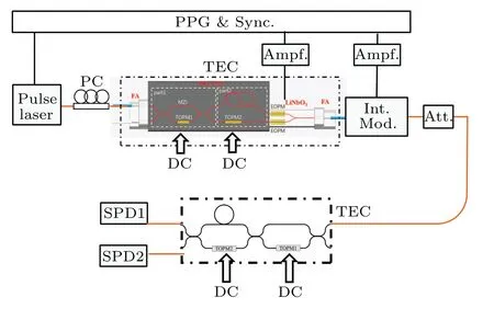
Fig. 5. Schematic diagram of QKD system based on hybrid chip at Alice and silica AMZI chip at Bob. PC:polarization controller;TEC:temperature controller; DC: direct current source; PPG&Sync: pulse pattern generator and synchronization clock; Ampf.: RF amplification; Int. Mod: LN intensity modulator; Att.: off-chip optical attenuator; SPD: gated mode single photon detector.
The Alice section includes a pulse laser, a polarization controller, the hybrid chip, an off-chip LN intensity modulator, and an off-chip attenuator, in sequence. The Bob section includes SPDs and an silica AMZI chip,[26,27]with the identical temporal delay of Alice. Pulse pattern generator (PPG)provides the system clock to synchronize all the devices including pulse laser and SPDs. The driving signal from PPG is amplified by the radio-frequency(RF)amplifier,up to 3-dB bandwidth of 10 GHz with a 26-dB gain,to drive the EO modulator in the hybrid chip. Direct current source is used to drive the TOPMs in both Alice and Bob chips
5.1. Phase basis states|+〉and|-〉
We input to the system the pulses of 50-ps duration at 156.25-MHz repetition rate. We set the attenuator so thatμ=0.1. The Alice and Bob chips are separately temperaturecontrolled according to what we discussed in Section 2. We set the TOPM of tunable DC in both Alice and Bob chips to make intensity-balanced for WCPs. The system output generates three time slots in SPDs. Interference occurs in the middle time-slot,named S2,allowing the states|+〉and|-〉to be measured.
The interference fringesversusPPG driving voltage are shown in Fig. 6(a). It can be seen that the curve profile is sine-like within 0.66 Vpp, beyond which the curve becomes flat due to the saturation of the RF amplifier. The relative phases between WCPs are 0 andπcorresponding to 0.1 Vpp and 0.62 Vpp,respectively. When the voltage is 0.1 Vpp,the output count at S2 is 0.28×10⁵for SPD1 and 2.02×10⁵for SPD2. When the voltage is 0.62 Vpp, the output count at S2 is 2.38×10⁵for SPD1 and 0.19×10⁵for SPD2. The interference visibility,V=(max-min)/(max+min),is 78.53%for SPD1 and 82.68% for SPD2. The histograms of three time slots are scanned as shown in Figs.6(b)and 6(c)corresponding to 0.1 Vpp and 0.62 Vpp, respectively. Next, we conduct the research on the phase stability. We keep the voltage at 0.62 Vpp, The ratio between outputs of both SPDs at S2 is recorded every 3 min over 8 h. Figure 7 shows the plot of the ratio variationversustime. It can be seen that most of values vary from 4 dB to 8 dB.
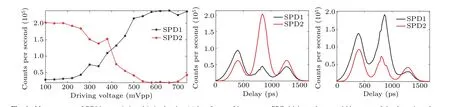
Fig. 6. Measurements of BB84 states |+〉 and |-〉, showing (a) interference fringe versus PPG driving voltage, and histogram of the three time slots corresponding to(b)0.1 Vpp and(c)0.62 Vpp,respectively.
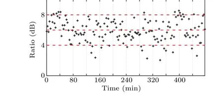
Fig. 7. Test of phase stability, indicating ratio between two outputs versus time,with voltage fixed at 0.62 Vpp.
Next we will discuss the visibility and phase stability shown by our system.The visibility is related to the ratio given in Ref.[27]

whereN1andN2are the photon counts of two interfering pulses and ΔφModeis the modal phase mismatch. The interference visibility is relatively low. For that there are two major reasons. One reason is that the increase of driving voltage breaks the intensity-balance of WCP.As can be seen from the SPD2 (red curve) in Figs. 6(b) and 6(c), the count ratio between the first and final times lot dramatically changes when the driving voltage changes from 0.1 Vpp (N1=N2)to 0.62 Vpp (N1/=N2). The increase of voltage breaks the count balance betweenN1andN2, thus reducing the visibility. The other reason is that the temperature of Bob chip is not optimal due to TEC limitation. At this temperature point,the TE mode and TM mode are not perfectly in phase, namely,ΔφMode/=0,thus leading to none-perfect interference and low visibility. It is promising to improve the visibility in these two aspects by compensating for the imbalance of intensity and upgrading TEC to cover the optimal AMZI temperature. Besides, the relative phase between WCPs is unstable. The reason is that the LN EO phase modulator is quite polarization sensitive. Therefore the interference is very sensitive to the fluctuation of driving signal or the fiber stress change.
5.2. Time-bin basis states|0〉and|1〉
With the aid of an extra off-chip LN intensity modulator as shown in Fig. 5, we prepare states|0〉and|1〉for the time-bin basis. Figure 8 illustrates a histogram of the states’generation before Bob(left column)and the corresponding final measurement outcomes on both SPDs(right two columns).Measurement in the first time slot (S1) of either SPD output represents a|0〉and a measurement in the third time slot(S3)is|1〉. The extinction ratio ERtimefor state|0〉(or|1〉) can be represented by the ratio in dB of sum of both SPD outputs at S1(or S3)to the counterpart at S3(or S1). Therefore ERtimeis 18.65 dB for state|0〉and 15.46 dB for state|1〉. It is worth noting that the two SPDs cannot achieve the balanced WCP simultaneously. In this case the SPD2 has nearly balanced counts at the two time slots while SPD2 has not. This is because the ending DC of AMZI at Bob is not perfectly 3 dB.This can be optimized by scanning and finding the optimal coupling length of DC in the fabrication process.

Fig.8. Measurements of BB84 states|0〉and|1〉. Measurement in slot S1 of either SPD output represents a|0〉and a measurement in slot S3 is|1〉.
6. Asymptotic secure key analysis
We perform an asymptotic secure key estimation based on the visibility and extinction ratio ERtimemeasured in our case.Since our circuit does not include another intensity modulator that is required for the use of decoy states. We therefore use a security proof,[28]to provide security against general attacks in the case of non-phase-random,non-decoy state BB84,with the key rate per pulse given by

whereILBob, the excess loss of Bob AMZI chip, is measured to be 2.48 dB,α=0.2 dB/km is the loss coefficient of single mode fiber andLis the fiber length. Hereεis the quantum bit error rate (QBER) observed in the verification test, andf(ε)≥1 is the error correction inefficiency used to perform key reconciliation(heref(ε)=1.22 according to the literature estimate value).H2(ε)is the binary Shannon entropy given by

where the factor of 1/2 in each term on the right-hand side is related to the random basis selection of 50%possibility. The QBERphaseis due to imperfect phase state and given by

wherepdarkis the probability of recording a dark count per time gate and per detector. In our case,pdarkis 3×10⁻⁶/gate.Then=2 is the number of detectors. It is clear that QBERdetincreases with distance,since the dark-count rate remains constant while the bit rate comes down liketlink.
It is worth noting that the fluctuation of the phase state can also increase the QBER.The analysis of this factor is also out of our experimental capability. Fortunately, our AMZI chips are capable of actively compensating for the phase variation.The TOPM in the AMZI can be used to actively compensate for the phase fluctuation. An online feedback procedure,[22]based on the TOPM has been demonstrated by some researchers to implement the compensation, showing good effect on reducing the QBER.
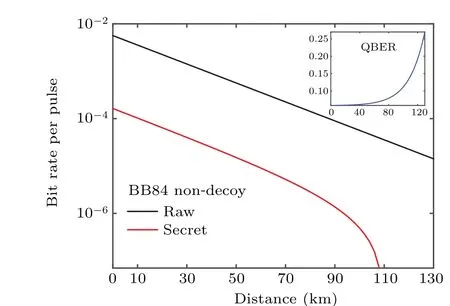
Fig. 9. Estimated asymptotic secret key rate and relevant QBER for nondecoy BB84 QKD.
The raw keyRequation (3), secret keyKBB84equation (2), and QBER equation (8) are plotted against the distance as shown in Fig. 9. A secure key rate of 10.041 kbps(6.4265×10-5bit per pulse)is expected at 156.25-MHz repetition rate over a 20-km distance with an estimated QBER of 0.059.
7. Conclusions and perspectives
In this work,we design and prepare a BB84 QKD transmitter based on hybrid-integration of silica and LN chips.Four BB84 states are encoded and decoded at a repetition rate of 156.25 MHz. The interference fringe visibility is 78.53%for phase state|+〉and 82.68% for phase state|-〉. The extinction ratio is 18.65 dB for time-bin state|0〉and 15.46 dB for time-bin state|1〉. An asymptotic estimated secure key rate of 10.041 kbps is expected over a 20-km distance with an estimated QBER of 0.059. We give several possible reasons for the low visibility and low-stability that our system shows,based on which future work is needed to improve the performance.
Acknowledgements
Project supported by the National Key Research and Development Program of China(Grant No.2018YFA0306403),the National Natural Science Foundation of China (Grant Nos. 61435013 and 61627820), the Strategic Priority Research Program of the Chinese Academy of Sciences (Grant No.XDB43000000),and the K.C.Wong Education Foundation, Anhui Initiative in Quantum Information Technologies,China(Grant No.AHY030000).
猜你喜欢
作文小学高年级(2022年4期)2022-05-27
少年文艺·我爱写作文(2022年4期)2022-05-12
初中生学习指导·中考版(2022年4期)2022-05-12
湖南水利水电(2021年6期)2022-01-18
音乐天地(音乐创作版)(2020年9期)2021-01-14
书香两岸(2020年3期)2020-06-29
中国篆刻(2019年8期)2019-08-14
红领巾·成长(2018年10期)2018-11-19
凉山文学(2018年1期)2018-01-16
中国农村科技(2014年5期)2014-04-18
- Chinese Physics B的其它文章
- Ergodic stationary distribution of a stochastic rumor propagation model with general incidence function
- Most probable transition paths in eutrophicated lake ecosystem under Gaussian white noise and periodic force
- Local sum uncertainty relations for angular momentum operators of bipartite permutation symmetric systems
- Quantum algorithm for neighborhood preserving embedding
- Vortex chains induced by anisotropic spin–orbit coupling and magnetic field in spin-2 Bose–Einstein condensates
- Short-wave infrared continuous-variable quantum key distribution over satellite-to-submarine channels