
Progress of Pb-Sn Mixed Perovskites for Photovoltaics:A Review
2022-07-04 09:12RajapaksheMudiyanselageIndrachapaBandaraShashiniSilvaCameronUnderwoodImalkaJayawardenaRaduSporeaandRaviSilva
Energy & Environmental Materials 2022年2期
Rajapakshe Mudiyanselage Indrachapa Bandara , Shashini M. Silva, Cameron C. L.Underwood , K. D. G. Imalka Jayawardena , Radu A. Sporea , and S. Ravi P. Silva*
1. Introduction
Inorganic–organic hybrid metal halide perovskites have shown great promise in high-performing photovoltaic devices with low fabrication cost. In this regard, Pb-Sn mixed perovskites are considered as highly suitable candidate for all-perovskite tandem solar cells[1-6]and singlejunction solar cells with narrow bandgaps.[7-9]However,the maximum performances of Pb-Sn mixed perovskite solar cells(PSCs)have not yet been achieved due to the limited understanding of the material system as well as prevailing issues due to unintentional material doping through Sn oxidation.
The increasing popularity of Pb-Sn mixed perovskite absorbers,whether in tuning the bandgap[10]or reducing the toxic Pb content,[3,11]is due to the ease of Sn incorporation in the B site of the ABX3crystal structure (where A = monovalent cation, B = divalent metal cation, X = halide ion) considering the similar qualities of Sn and Pb.These group 14 elements have comparable ionic radii in the +II oxidation state enabling Sn2+to occupy the B site in a similar manner to Pb2+without deteriorating the perovskite lattice.[12]By tuning the Pb:Sn ratio,the inherently lower bandgaps of Pb-Sn mixed perovskites can be tuned around 1.2 eV – 1.3 eV range[1,2,11-31]that Pb-only perovskites fail to approach[32](Figure 1). This makes them attractive candidates for the bottom cells(narrow-bandgap cells; to absorb low-energy photons) of all-perovskite tandem solar cells,enabling a theoretical maximum efficiency of 37%.[1-3,6]Single-junction Pb-Sn cells can also achieve a bandgap closer to the ideal Shockley–Queisser limit(~1.3 eV).[1-3]In addition,it has been reported that the charge carrier mobility of Sn perovskites can be superior than that of the Pb counterparts.[33]
However, compared to their Pb-only counterparts which have already reached singlejunction power conversion efficiency (PCE) of 25.5%, Pb-Sn mixed perovskites have achieved lower efficiencies, the maximum being just over 21%.[12,34]Currently,this limits the maximum performance practically achievable through all-perovskite tandem solar cells.Thus,a better understanding of Pb-Sn perovskites is currently required,which has driven a notable quantity of research effort by many researchers worldwide.[35-38]It is common knowledge that a significant challenge in Snbased perovskites is the oxidation of Sn2+to its more stable form Sn4+,producing a large number of vacancies and defects, thus destabilizing the perovskite structure.[30,31]Various efforts have been made to tackle this issue in the route to achieving high efficiencies in these cells. The first incorporation of Sn2+in Pb2+perovskite to compose a Pb-Sn mixed PSC device with a planar architecture was reported in 2014 by the Jen group[12]of Washington University,USA(which yielded a PCE of 10.1% for a MAPb0.85Sn0.15I3composition). By late 2020, the efficiency of single-junction planar Pb-Sn mixed PSCs has reached over 20%[34,39-45]the maximum being 21.1% and 21.7% (certified PCE 19.5% and 20.7% respectively) from the Tan group[34,45](Nanjing University,China),via tackling the Sn2+oxidation issue successfully.In 2019,the authors reported the use of metallic Sn to reduce Sn4+vacancies in a MA0.3FA0.7Pb0.5Sn0.5I3system (MA = methylammonium, FA= formamidinium).[34]In 2020, their most recent report employed a zwitterion(FSA;formamidine sulfinic acid)antioxidant to inhibit Sn4+oxidation while achieving surface and grain defect passivation, giving rise to the maximum efficiency of 21.7%reported for Pb-Sn cells up to date.[45]In comparison, the Sn-only (Pb-free) PSCs have reported a highest PCE of 13.24% so far where Nishimura et al.[46]incorporated ethyl ammonium (EA) in a GeI2-doped FA0.98EDA0.01SnI3perovskite(EDA = ethylenediammonium) to reduce lattice disorder while improving the charge career mobility and surface passivation to reduce traps and defects.

Figure 1. Bandgaps of Pb-only(blue) and Pb-Sn mixed (red) perovskites with different compositions reported in recent years. Reused with permission.[123] Copyright © 2018, American Chemical Society.
The progress of single-junction Pb-Sn mixed PSCs so far is given in Figure 2, in terms of their device parameters; VOC(open circuit voltage), JSC(short circuit current density), and FF(fill factor) as a function of their PCE. In most high-performing PSCs, enhancements of all the said parameters are noticeable.The VOCof majority of Pb-Sn PSCs lies well below 1.0 V even in the highest performing devices whereas the JSChas easily reached over 30 mA cm−2, owing to the lower bandgaps of the photoactive layer. Due to inherent issues with Sn4+traps and defects, the fill factors of Pb-Sn devices are mostly around 80%.Thus, for PCE enhancements, the VOCand FF should be further enhanced. However, VOCimprovements commonly lead to compromising the JSC;thus, the FF should be given close attention in further device developments. To fine-tune the optoelectronic properties and performance, various methods have been explored such as engineering the ionic composition of the ABX3crystal structure, fabrication methods, and device interlayers.[37,47]In the majority of these studies, an inverted (p-i-n) device architecture is preferred over a standard (n-i-p) architecture in order to allow better matching of interlayer band energies and more importantly, to mitigate the degradation of the Sn-based perovskites due to dopants added to the charge transport layers.
The device structure, perovskite composition, and the pre/posttreatments play interactive roles with each other to affect the final device performance.Given the increasing interest in the field,a comparison of the many different approaches taken toward enhancement of Pb-Sn mixed perovskites is currently crucial to achieve the maximum efficiency possible from the photovoltaic (PV) devices. Thus, this review comprehensively discusses the evolution and engineering of Pb-Sn mixed PSCs, concluding reports from 2016 to 2020 (both singlejunction cells and narrow-bandgap cells developed for perovskite tandem devices).First,the PSC device operation is explained,followed by the device architectures and interlayers used in Pb-Sn mixed perovskites. Next, the perovskite absorber layer is discussed in detail,including various reports on fabrication methods and fine-tuning of the perovskite film and the absorber bandgap. Lastly, the most prominentefforts in addressing the Sn4+issue and further surface passivation of the Pb-Sn mixed perovskites are summarized, including the reports on maximum efficiencies achieved so far. This work aids in better understanding the interplay among the various parameters affecting the Pb-Sn mixed PSC performance and paves the way in further developments toward maximizing the device efficiencies.

R. M. Indrachapa Bandara received her Ph.D. in photovoltaics from the Advanced Technology Institute, University of Surrey, UK (2016-2019), in inorganic–organic hybrid Pb-Sn mixed perovskite solar cells. She is currently a postdoctoral researcher in the Advanced Technology Institute developing robust and high-performance organic/polymer thin-film electronic devices for high-speed, high-throughput, and low-cost roll-to-roll printing. Prior to obtaining her doctorate, she received her BSc (Hons) in Chemistry from the University of Cincinnati, USA, and was employed as a Research Scientist in Sri Lanka Institute of Nanotechnology, and a Process Assistant in Warwick Manufacturing Group.

Shashini M. Silva graduated from the University of Moratuwa, Sri Lanka, with a BSc(Hons) Materials Science and Engineering (2013–2017). She is currently a doctoral research student at the Advanced Technology Institute of the University of Surrey, UK (2019–present),working on organic–inorganic Pb–Sn mixed perovskite materials for high-performing photovoltaic devices. Her primary research focus is on fabrication of Pb–Sn mixed perovskite solar cells with high performance in terms of stability and high reproducibility that is on par with that of lead-only perovskites.

Cameron C. L. Underwoodreceived an MPhys degree in Physics from the University of Surrey in 2017 and completed his Ph.D. research in Electronic Engineering in 2020 at the Advanced Technology Institute. His doctoral work focused on the ab Initio Calculations of the Structural and Electronic properties of Snbased Perovskite solar absorber materials. He is now a postdoctoral researcher at the Advanced Technology Institute, conduction further computational work on electronic properties of various 2D and 3D perovskite materials
2. The Perovskite Solar Cell
2.1. Operation Principles of PSC Devices
2.1.1. Charge Carrier Photogeneration
PSCs fall under“non-excitonic”systems due to the nature of the charge carriers generated.[48,49]Thin-film PV devices can be excitonic or nonexcitonic, where the latter is considered more advantageous. An excitonic system such as an OPV cell (organic photovoltaics) generates excitons(electron-hole pairs bound by Coulombic forces of~300 meV binding energy) in the photoactive layer upon absorbing photons.[50-52]For the cell to generate a current,the bound charges have to overcome the large binding energy and dissociate into free carriers.[50,51]As such, energy requirements for exciton diffusion and dissociation limit the performance of excitonic PV devices.[50,53]PSCs and other non-excitonic systems such as Si,CdTe,and CIGS(copper indium gallium selenide) photon absorption directly generate free electrons and holes.Although the nature of metal halide perovskite charge generation was speculative at first, studies have shown that the generic exciton model is not a satisfactory fit for perovskites.[49,53]A more accurate way of describing this is that the perovskite generates electron-hole pairs with<50 meV binding energies(for Pb-only),enabling them to dissociate completely to act as free carriers at room temperature,comparable to direct bandgap inorganic semiconductors.[49,53-55]For,MAPb1-xSnxI3perovskites this was reported to be <16 meV by Galkowski et al, proving that Pb-Sn mixed 3D perovskites are also nonexcitonic systems.[56]Thus,Pb-Sn mixed perovskites enjoy the benefits of mitigating exciton diffusion and dissociation energy losses,[50]while allowing solution processability, thin-film PV device fabrication, and bandgap tunability.Since they exhibit intrinsic semiconductor properties,the fundamental PSC device architecture is a p-i-n(or n-i-p)junction diode (similar to amorphous Si cells).[57,58]Here, the p-type semiconductor is the hole transport layer (HTL) and the n-type is the electron transport layer(ETL),[48,50]where the n-i and p-i heterojunctions selectively extract electrons and holes.[53]
2.1.2. Charge Transport and Extraction
For a functional PV device,the photogenerated charges should then travel through to an external circuit.As discussed above,a PSC consists of a p-i-n or n-i-p diode(discussed further in Section 2.2.1).To complete the device anode and cathode, highly conductive contacts are formed on either side of this structure as shown in Figure 3a,which allow the charges to enter an external circuit.In a typical PSC,one of the contacts is a transparent electrode (deposited on a glass or transparent plastic substrate)to allow visible light to enter the photoactive layer,while the other is a highly reflective metal electrode.[59]The charge carriers first travel through the perovskite to the p-i or n-i interface, governed by the charge carrier mobilities of the perovskite. Typically, the sum of electron and hole mobilities of perovskites range around 10 - 30 cm2V−1s−1(determined through terahertz mobility measurements),[60]significantly higher in comparison with other solution-processed PV materials(e.g.,OPVs~10−3–10−4cm2V−1s−1).[50]The closely comparable electron and hole mobilities of perovskites[61]ease the charge transport under the built-in-potential, preventing charge accumulation(space charge).[62]The carrier mobility also decides the thickness of the perovskite layer in the PSC to achieve balance between charge generation and extraction.

K. D. G. Imalka Jayawardena is the Marcus Lee Lecturer at the Advanced Technology Institute at the University of Surrey. His research focuses on the development of multijunction solar cells based on perovskites, developing new detectors for medical imaging and radiation dosimetry, and understanding radiation damage in materials. He received his Ph.D. from the University of Surrey working on gas sensors and his BSc (Hons) in Engineering from the University of Moratuwa, Sri Lanka. Following his PhD, he has worked on organic and perovskite photovoltaics (supported by the EPSRC Doctoral Prize award) and also on organic–inorganic hybrid X-ray sensors.

Radu A. Sporea is a lecturer(assistant professor) in Power Electronics and Semiconductor Devices at the Advanced Technology Institute, University of Surrey. He holds an EPSRC Early Career Fellowship(2021-2026). Prior to this, he was a Royal Academy of Engineering Academic Research Fellow, EPSRC PhD+ Fellow and Ph.D. researcher at the same center. Before Surrey, Radu studied Computer Systems Engineering at “Politehnica” University, Romania, and worked as an Engineer for Catalyst Semiconductor Romania. He currently leads a research team focused on energy-efficient, large are electronics, covering applied materials, advanced electronic devices, circuits, and their applications to sensors systems and user interfaces.

S. Ravi P. Silva CBE FREng is a Distinguished Professor and the Director of the Advanced Technology Institute at Surrey University. He joined Surrey after completing undergraduate and postgraduate degrees at Cambridge University. His research interests include nanotechnology and renewables and have resulted in over 580 papers: with 20,000 citations,an H-index 72, 35 patents and has won research funding over£40 M. He is a Fellow, Royal Academy of Engineering, UK,

Figure 2. Progress of single-junction champion Pb-Sn mixed PSCs (laboratory tested values) reported so far with the device parameters VOC, JSC, and FF plotted against the device PCE. The Sn content (x) and A-site cation composition are shown in different colors and symbols.
At the respective interfaces, the ETL and HTL extract the free electrons and holes provided that the conduction band (CB) and valence band (VB) of the perovskite layer align with the lowest unoccupied molecular orbital(LUMO)or the CB of the ETL,and the highest unoccupied molecular orbital (HOMO) or the VB of the HTL, respectively(Figure 3b).[50]
The ETL and HTL in turn should form Ohmic contacts with the electrodes(highly conductive contacts)which is decided by the work function of the electrodes.[59]As such,the interfaces play an important role in the function of a PSC and can contribute to losses through non-radiative recombination and charge transport barriers as a result of energy mismatch[59]and thus should be properly engineered.[63]Proper selection of electrodes and interface materials (interlayers) for Pb-Sn PSCs will be discussed next in Section 2,and the perovskite absorber layer will be further discussed in Section 3.

Figure 3. a) Schematic illustration of a solar cell stack. b) Schematic of the mechanism of working PSC under illumination.The photogenerated charge carriers drift to the interlayer interfaces,where the electrons transfer to the ETL and holes transfer to HTL, given that there is a proper match of the energy levels. The charges are then transported to the respective electrodes,to be extracted into an external circuit.
2.2. Device Architectures and Interlayer Materials for Pb-Sn Mixed PSCs
2.2.1. Device Architectures
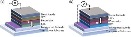
Figure 4. Schematic illustrations of PSC device architectures of a) standard / n-i-p and b) inverted /p-i-n configurations, at forward bias. The direction of electron flow is shown by the arrows.
A PSC device can be either of the “standard/regular” (n-i-p) architecture; with the sequence of transparent cathode/ETL/perovskite/HTL/metal anode, or of the “inverted”(p-i-n) architecture; with transparent anode/HTL/perovskite/ETL/metal cathode sequence.[63]Although in Pb-only PSCs with record efficiencies, the standard architecture is commonly reported (Figure 4a),[48]the inverted configuration is most widely used in Snbased or Pb-Sn mixed PSCs[15,64](Figure 4b), which allows better suitability for low-temperature device fabrication. The charge transport layers used in the inverted configuration are mostly inspired by OPVs (such as polymers and fullerene derivatives) suited for lowtemperature large area PVs.[15,64]Thus, Pb-Sn PSCs, this limits the use of doped HTL layers such as Spiro-OMeTAD which is commonly used in Pb-only standard device,[65]alleviating any dopant induced in the highly reactive Sn-incorporated perovskites.
2.2.2. Electrode Materials
The common electrode materials and charge transport materials for PSCs are given in Figure 5. While it is necessary that one of the electrodes has high light transmission (front contact), depending on the application,the back contact electrode can also be made semi/transparent.[66,67]However, in single-junction Pb-Sn PSCs, the back contacts are still made of highly reflective metals which also serves the function of reflecting the light back toward the perovskite layer.Typical Pb-only PSCs employ thin films (~100-150 nm) of Au or Ag,[63]and Pb-Sn mixed PSCs mostly use Ag[1,11,14]and in some cases Al[2,20,68]electrodes,owing to their high reflectivity and suitable work functions(Ag~4.3 eV and Al~4.2 eV)that align well with fullerene-derived ETLs.In one study on all-inorganic Pb-Sn mixed PSCs by Liang et al,[22]a carbon electrode was employed to replace the metal back contact as well as the HTL in a standard device architecture. The authors achieved a very high VOCof 1.26 V with a CsPb0.9Sn0.1IBr2absorber,while avoiding unstable organic components for HTL and expensive noble metal electrodes. Use of Cu electrodes has also been reported by the Tan group,[34,45]resulting in 21.1% and 21.7% efficient MA0.3FA0.7Pb0.5Sn0.5I3PSC; however, these high efficiencies were attributed by the authors to other modifications of the cell and not the choice of electrode metal alone. The transparent electrode in a PSC is typically a conductive oxide layer such as ITO (indium-doped tin oxide) or FTO (fluorine-doped tin oxide) given their high light transmission, conductivity, and reproducibility[59,66](apart from PSCs, ITO is employed in OPVs,microcrystalline Si cells and CIGS,and FTO in a-Si cells, DSSCs (dye-sensitized solar cells) and CdTe PVs).[69]The vast majority of Pb-Sn-mixed and other low-temperature processed inverted PSCs employ ITO,[11,16,17,59,64]although a limited number of studies also employed FTO electrodes.[30,36]ITO electrodes are attractive candidates for flexible PSCs (ITO-coated PET (polyethylene terephthalate)and PEN (polyethylene naphthalate substrates),although flexible Pb-Sn mixed perovskites are not yet reported widely. FTO needs highprocessing temperatures, limiting its suitability to be deposited on plastic substrates. However,in some cases indium diffusion into the adjacent layers was reported with ITO,[70]whereas FTO has more stability (against high temperatures and physical abrasion), thus more suited for Pb-only standard devices which requires high-processing temperatures of ~400-500°C for ETL deposition(e.g.,TiO2).
Contrary to the popular use, Kapil et al. replaced ITO with FTO in inverted PSCs with a (CsxFA1−xSnI3)0.5(MAPbI3)0.5absorber to find higher external quantum efficiency (EQE) reaching 80% at 900 nm.[71]The authors point out that the widespread assumption that high surface roughness of FTO may lead to short circuits in the device,may have limited the use of FTO in Pb-Sn mixed PSCs, and highlight the benefit of FTO in allowing higher light transmission in the NIR region. Over 800 nm, Pb-Sn PSCs in this work exhibited higher JSC(improving overall from 29.1 mA cm−2to 31.58 mA cm−2) increasing the PCE from 16.7%to 17.7%.[71]
2.2.3. Charge Selective Layers
Electron Transport Layers: Solution-processable ETL materials can be either inorganic (mainly transition metal oxides), or organic materials (fullerenes and derivatives),[72]where the latter is used in most of the Pb-Sn mixed PSCs (Figure 5). A high-electron mobility and proper energy-level alignment with the perovskite CB are vital in selecting a suitable ETL.[73]
Inorganic ETLs: Transition metal oxides were initially used in DSSC technology and widely seen now in standard PSC architecture.[63]In high-performing Pb-PSCs,the first and most common inorganic ETL is TiO2owing to its high-electron collection efficiency. In Pb-Sn PSCs however, TiO2can only be seen in a few very early reports[10]and in all-inorganic Pb-Sn PSCs.[22]Its need for very high temperatures(~400– 500 °C) in fabrication,[74]instability under UV exposure, and lowelectron mobility hinders widespread commercial applications.[73,75]Therefore, other transition metal oxides such as ZnO[76]and SnO2[77]are employed (cast from nanoparticle solutions) in Pb-PSCs as alternatives to TiO2, of which the former was also adopted for Pb-Sn mixed PSCs.[7,47,78]ZnO can be used to improve the band alignment between the metal electrode and fullerene-based ETLs or as an optical spacer, is solution processable at room temperature, and does not need further annealing.[47]Despite the attractive qualities of ZnO, the long-term chemical instability hinders its application.[79]In contrast, SnO2,although not widely explored in Pb-Sn PSCs, has higher stability in ambient conditions and needs relatively low fabrication temperatures of~180°C.[79]SnO2-EDTA (ethylenediaminetetraacetic acid) complexes were also reported in Pb-only devices as means of reducing the hysteresis in devices with this ETL,[80]which resulted in record efficiencies of 21.5%for a FA0.95Cs0.05PbI3containing PSC.
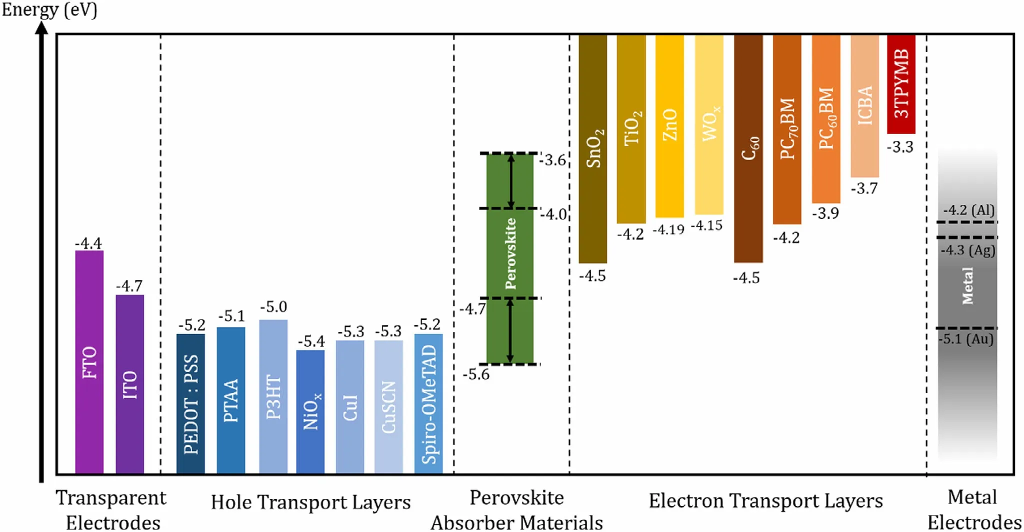
Figure 5. Energy levels (with respect to the vacuum level) of different layers used in PSCs.[187-189] From left: work functions of transparent electrodes, HOMO levels or work functions of HTLs, VB and CB levels of reported perovskites (VB can be tuned roughly between −4.7 and −5.6 eV and CB between −4.0 and−3.6 eV), LUMO levels of ETLs, work functions of metal electrodes.
Organic ETLs: Organic ETLs were inspired by OPVs and are widely used in Pb-Sn mixed PSCs, of which the most common are fullerenes such as C60[13,15,68,81]and bis-C60[9,25,27,28]and their derivatives such as PC60BM([6,6]-phenyl-C 61-butyric acid methyl ester),[8,78]PC70BM([6,6]-phenyl-C 71-butyric acid methyl ester),[7,47]and ICBA(indene-C60bisadduct).[9,28]Additionally, some have reported other organic molecules such as Phen-NaDPO.[82]A proper match between the perovskite CB and the LUMO of the organic ETL has to be ensured for efficient electron extraction. A comparative study on 6 different fullerene derivatives as ETL was reported by Lin et al., employing Pb-Sn PSCs with a MAPb0.5Sn0.5I3perovskite absorber (Figure 6).[19]The authors reported a strong dependence of device VOCon the LUMO level of the fullerene derivative used. From the tested ETLs, the novel fullerene derivative BPB-M showed the best results with a PCE of 10.24%(JSC22.8 mA cm−2, VOC0.69 V and FF 65%) followed by PCBM and C60. These have LUMO levels of −3.74, −3.68, and −3.78 eV respectively (relative to vacuum level), lower than the CB of MAPb0.5Sn0.5I3perovskite (−3.67 eV relative to vacuum level) as depicted in Figure 6b.
In Pb-Sn mixed PSCs, both C60and its derivatives are considered good ETL candidates with low-temperature and large area processability, excellent band alignment, and sufficient electrical conductivities,although their electron mobilities are considerably inferior to inorganic materials.[63,72]Pb-Sn mixed PSCs often use two or more organic ETLs are used together,through sequential deposition of C60or bis-C60with PCBM or ICBA.[9,11,26,28]In some cases,C60was employed as a surface passivation layer,[36]which reportedly reduced the pinholes on perovskite film, passivated the perovskite-ETL (PCBM) interface, and protected the perovskite from exposure to oxygen and moisture.Employing several ETLs together also allows favorable band alignment in PSCs, depending on the perovskite CB, and improves efficiency of electron extraction. In other reports, PC60BM surface was coated with inorganic materials such as ZnO (nanoparticles),[78]metal-organic materials such as Zr-Acac,[21]or other organic materials such as Na-DPO,[82]to compose the ETL.
Furthermore, in many Pb-Sn mixed PSCs,a thin (~5-7 nm) film of bathocuproine (BCP) is typically employed as a buffer layer at the ETL/electrode interface.[15,30,36,68,83]BCP is an organic small molecule material, used as an “interlayer” for improvement of interfaces which critically affect the charge transport and recombination dynamics in PSCs and OPVs.[83]It is reported that BCP aids in improving the metal electrode and organic ETL contact through reducing charge accumulation at this interface and reducing recombination.[83,84]The vast majority of Pb-Sn mixed PSCs employ PCBM/BCP/Ag or C60/BCP/Ag to comprise the device cathode. Inorganic interface layers such as LiF[19]and Al-doped ZnO[7,47]have also been reported in some cases for Pb-Sn mixed perovskites.
2.3. Hole Transport Layers
The solution-processable HTLs can also be either inorganic or organic materials (Figure 5), with the latter being most regular for Pb-Sn mixed PSCs. In standard Pb-based PSCs, the most popular HTL is the organic small molecule Spiro-OMeTAD (2,2′7,7′-tertrakis(N,N-pdimethoxyphenylamino)-9,9′-spirobifluorene) system,[85]which was initially explored for Pb-Sn PSCs in very early reports (standard device architecture).[10]To enable better conductivity, Spiro-OMeTAD needs to be partially oxidized by a combination of dopants (LiTFSi(lithium bis(trifluoromethanesulfonyl)imide), TBP (tributyl phosphate), and FK209 (tris(2-(1H-pyrazol-1-yl)-4-tert-butylpyridine)cobalt(III)),[64,86]which can give rise to degradation of the perovskites through reacting with the I−ions,despite the high performance of the HTL.[87]This effect is much severe in Pb-Sn mixed perovskites and other Sn-incorporated perovskites, due to their inherent high reactivity.[65]Therefore, it is best that Pb-Sn mixed PSCs (as well as Sn-only)to employ HTLs that do not necessitate doping,[65]and as such,PEDOT:PSS (poly(3,4-ethylenedioxythiophene):poly(styrenesulfonate))is commonly used in this field.[28,45,88]

Figure 6. a) Device schematic of PSCs with MAPb0.5Sn0.5I3 absorber and fullerene derivatives as ETL. b)Energy diagram of various device layers, drawn relative to vacuum level set to zero by definition. c) J-V characteristics of devices under AM 1.5G simulated solar irradiation of 100 W m−2 with a fixed scan rate of 50 mV s−1 (no stabilization done prior to measurement). d) IPCE (EQE) spectra for devices. e)Molecular structures of the fullerene derivatives employed as ETL. Reproduced with permission.[19]Copyright © 2016, Elsevier.
PEDOT:PSS is a conductive polymer blend with a work function of ~5.1-5.2 eV, initially used in OPVs. The suitable work function alignment with perovskite absorbers, water solubility enabling easy ambient processing without toxic solvents, and large area processability has made this material attractive in inverted PSCs. Despite the inherent acidity of PEDOT:PSS which reportedly induce corrosion of the ITO electrode,[89]it is still the preferred HTL in many Sn-incorporated PSCs[65]since it is sufficiently conductive to avoid dopants. However, PEDOT:PSS has also been infamous for its role in giving rise to poor morphology of perovskite layers (high defect density from pinholes and open grain boundaries), and inferior interface band alignment resulting in poor electron blocking capability.[8,9,78,81]Moreover, in Sn-containing perovskites, any residual water in the PEDOT:PSS layer can accelerate Sn2+oxidation. Thus,other organic polymers such as PCP-Na[81]and PTAA,[78]have been used as HTL in Pb-Sn mixed PSCs, as well as modification of the PEDOT:PSS layer itself. In these occasions, an increase in film quality of the perovskite absorber among other improvements was reported, in contrast to PEDOT:PSS, leading to device efficiency improvements.[78,81]In a study by Yao et al,[88](Figure 7a-c) PSC efficiency improvements were achieved by simply using a highly diluted PEDOT:PSS solution(1:8inIPA)asHTLfor MA0.4FA0.6Pb0.4Sn0.6I3cells.ThePCE improved from 17.79% (undiluted HTL) to 19.50% (diluted HTL, with a further optimized device of 19.58%) attributed to a more favorable energy-level alignment of the diluted HTL (work function −4.85 eV) with the perovskite VB level (−4.98 eV), than the undilutedPEDOT:PSS(workfunction−5.04 eV). In the recent work by Zhang et al,[90]PEDOT:PSS was modified with hydroquinone (HQ) to yield a 14.65% efficiency (from 13.85% of reference) for MA0.7FA0.3Pb0.7Sn0.3I3PSCs. Here, the HQ treatment was carried out in keeping with other reports that used p-dopants or high boiling point solvents to reduce sheet resistance of PEDOT:PSS and improve conductivity of the HTL.[90]The authors report a lower interface barrier between the HTL and the perovskite film, lower leakage current,and improved grain sizes of ~1 μm with HQ-modified PEDOT:PSS, with the maximum improvements achieved at 0.5 wt%HQ (in IPA) spin-coated on top of PEDOT:PSS.
In a study using an alternate organic HTL,PCP-Na, Shao et al[81]achieved a more compact, pinhole free film morphology for a FAPb0.5Sn0.5I3perovskite fabricated on the new HTL over a large area compared to the reference film on PEDOT:PSS, which effectively eliminated trap states and shunts reducing interfacial and bulk recombination.[81]The champion PCE was increased from 11.6%(PEDOT) to 16.27%(PCP-Na) with significant improvements of all the device parameters (VOC, JSC,and FF from 0.61 V, 27.80 mA cm−2and 68%(PEDOT) to 0.78V, 28.51 mA cm−2and 73%(PCP-Na))(Figure 7d,e), owing to the improved film quality as well as a more favorable energy alignment at the anode interface due to higher work function of PCP-Na. Furthermore, PEDOT:PSS morphology is reportedly of an isotropic nature while PCP-Na assumed a more crystalline structure with its backbone parallel to the ITO/substrate surface which allowed improved charge extraction.
In a study employing PTAA as the HTL,Wang et al achieved 13.6%PCE(compared to 9.6%for PEDOT:PSS reference)for a PSC containing FA0.7MA0.3Pb0.7Sn0.3I3double cation perovskite.[78]Here,the improvements were attributed to large (∼1 μm) perovskite grain growth on PTAA compared to the small grains on PEDOT:PSS with vertically aligned grain boundaries(Figure 7f).The more hydrophobic nature of PTAA reduces the surface tension dragging force and the number of nucleation sites available for the perovskite, resulting in high grain boundary mobility and larger grains. Perovskite layer grown on PTAA also resulted in a lower trap density, higher crystallinity, and higher hole mobility. In another study using PTAA as HTL, Chang et al[91]tested the effect of cross-linking and p-doping of PTAA for n-i-p devices with a MAPb0.75Sn0.25I3absorber and TiOx/PCBM ETLs. Here, TPEMN3 was used as the cross-linking agent and Mo(tfdCOCF3)3as the pdopant.Four types of HTLs(untreated PTAA,cross-linked PTAA,doped cross-linked PTAA, and Spiro-OMeTAD) were tested with resulting champion PCEs of 12.12%, 12.57%, 15.55%, and 13.31%, respectively,indicating the highest performance for doped cross-linked PTAA.Cross-linking under heating and light exposure was reported to form a 3D polymer network that increases the layer’s solvent resistance,maintaining the structural integrity of the film upon deposition of other layers of the PSC. The cross-linked PTAA also showed a higher light transmittance and no adverse impacts on the charge transport mechanisms of the perovskite films. Furthermore,it reportedly improved the device stability significantly, especially compared to the PSCs with Spiro-OMeTAD HTL. The p-dopant improved the conductivity of HTL by orders of magnitude, as well as shifting the HTL work function upwards,allowing better hole transport from the absorber to the HTL.
In parallel to polymeric HTLs, inorganic materials have also been explored as HTLs in Pb-Sn mixed perovskites to improve the stability and reproducibility of the resulting devices and to obtain high conductivity of the transport layer.In Pb-based perovskites,some of the inorganic HTLs used include NiOx,[92]CuI,[93]and CuSCN,[94]resulting in comparable efficiencies to Spiro-OMeTAD with better stability and reproducibility.Among those,NiOxwas employed in some reports for Pb-Sn mixed perovskites.[2,8,95]Zhao et al have employed a NiOx/PEDOT:PSS bilayer as the HTL in their work with MAPbxSn1-xI3PSCs,[2]which resulted in large micron-sized grains. Here, the NiOxlayer was casted on top of the PEDOT:PSS film to provide the base for the perovskite growth.The perovskite exhibited a low structural disorder and achieved full surface coverage. In other work, Chi et al reported the complete substitution of PEDOT:PSS with NiOxas HTL in FAPb0.75Sn0.25I3containing PSCs,[8]on the premise of NiOx’s ability to trigger perovskite crystallization and enhance hole extraction.The authors achieved compact,pinhole-free perovskite layers with larger crystals (~1 μm) on NiOxHTL compared to smaller crystal sizes and pinhole-rich perovskite growth on PEDOT:PSS(Figure 8a-d).The improvements were attributed to the inferior surface wetting properties of NiOxcompared to the highly hydrophilic nature of PEDOT:PSS. A more hydrophobic HTL surface is known to give rise to less nucleation sites resulting in larger grain growth.[8,78]The champion PCE of the devices with NiOxwas reported as 17.25%under reverse scan,compared to 14.24%for devices with PEDOT:PSS.Furthermore,devices exhibited low hysteresis and high stability(91%of initial PCE maintained at 80°C for 20 h,and 92%retained after 46 days at room temperature).Here,the NiOxfilm needed high-temperature annealing(300°C,1 h)to fabricate the HTL. However, a room temperature processed NiOxnanocrystal ink(L-NiOx)as HTL was reported in a very recent study by Chen et al (Figure 8e-i), resulting in highly efficient (champion PCE 18.77% and average 18.18 ± 0.30) MA0.4FA0.6Pb0.4Sn0.6I3PSCs with negligible hysteresis and high stability (96% retention of original PCE after 50 days under N2).[95]The authors compared these results against conventional high-temperature processed NiOx(H-NiOx, annealed at 250 °C) and reference PEDOT:PSS (annealed at 175 °C) containing devices which exhibited champion efficiencies of 15.85%and 17.03%,respectively. Here, L-NiOxHTL showed a deeper VB than the H-NiOx(Figure 8g), allowing better hole extraction from the perovskite layer,as well as slightly higher grain sizes and a lower trap density that decreased charge carrier recombination of the devices.The high quality and lower interface defect density of L-NiOxwere also ascribed to suppressing the Sn2+oxidation of the films,which translated to device stability.However,although no annealing of L-NiOxwas conducted in the fabrication process, the precursor nanocrystal ink preparation needed a 270 °C calcination step, whereas H-NiOxprecursor solution only needed 50°C.
3. Pb-Sn Perovskite Absorber
3.1. Crystal Structure
“Perovskites” (named after the Russian scientist Lev Perovski) have a general formula of ABX3, and a simple cubic unit cell comprising of a cations A and B(A > B)and anions X as depicted in Figure 9a.[96]The type of perovskites used in PSCs is“Metal Halide Perovskites”where X is a halide and B is a metal cation,[97,98]and have photoactive and semiconducting properties, with suitable bandgaps (~1-3 eV) suitable for photovoltaics and optoelectronic devices.[59,98]Here, as used in Pb-Sn perovskites,the A-site is a monovalent cation,either inorganic(such as Cs+)or organic(such as CH3NH3+(methyl ammonium or MA+),CH(NH2)2+(formamidinium or FA+),while X is commonly I−(although occasionally Br−and Cl−are incorporated).[97,98]The B-site cation in this case is a divalent group 14 metal cations Pb2+and Sn2+.[98]The ABX3structure is a combination of a cubic closely packed lattice of AX3(Figure 9a) and BX6octahedra stabilizing the B cation. The perovskite lattice has to achieve both charge neutrality and balance among the ionic radii, where BX6stability is decided by the “octahedral factor(μ)” (Equation 1), This takes ratio between the ionic radii rBand rXinto account, which should be between 0.442 and 0.895 for a stable perovskite structure.[98]

Another parameter,“Goldschmidt tolerance factor(t)”,factors in Asite cation radius rAEquation 2, and should be between 0.8 and 1.0.[98]

The ABX3crystal takes an almost ideal cubic structure when 0.9 < t≤1 (t = 1 ideal) and takes a tetragonal or orthorhombic structure under 0.8 < t < 0.9. Generally, t > 1 results when A-cation is too large and t < 0.8 when A is too small,both not allowing a structurally stable metal halide perovskite.
During the early developments of metal halide perovskites in PV,the focus was on MAPbI3as ABX3,but since then,the growing understanding of the chemical stability and the tunability of optoelectronic properties have led researchers exploring complex, mixed cation, and anion systems. The ionic radii of the common A sites mentioned above FA+(253 pm) > MA+(217 pm) > Cs+(188 pm), B-sites Pb2+(119 pm)> Sn2+(110 pm), and X sites I−(220 pm) > Br−(196 pm) > Cl−(181 pm)[98](Figure 9b) allow formation of perovskites with acceptable octahedral and Goldschmidt tolerance factors.
Although A, B, and X sites enable tuning of the perovskite bandgap, the band edges (the limits of the bandgap; CBminand VBmax) of the perovskite are formed by B and X molecular orbitals.[99,100]As such, A-site alterations do not directly affect the CB and VB of the perovskite, but rather controls the stability of the BX6octahedra by balancing the overall charge, and tunes the B-X distance through the size of the A-cation radius.[101]Thus, a large A-cation such as FA+will occupy more space in the perovskite lattice and decrease the B-X distance, thereby indirectly decreasing the bandgap (Figure 9c,d).[101]Similarly, a small cation such as MA+will increase the bandgap.
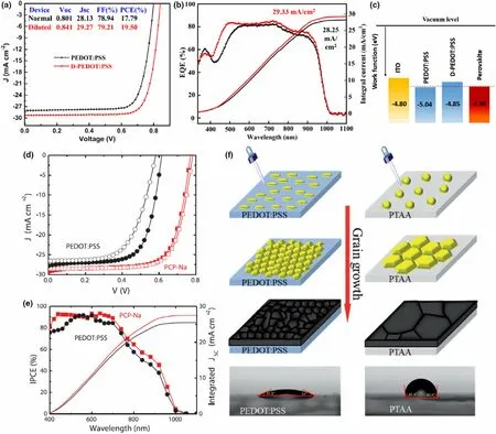
Figure 7. Enhanced electrical characteristics for PSC containing MA0.4FA0.6Pb0.4Sn0.6I3 absorber when PEDOT:PSS HTL was diluted by 1:8 in deionized water evident by a) champion J-V characteristics and b) EQE and integrated JSC of devices. c) Schematic image of electronic energy levels of ITO/PEDOT:PSS/perovskite layers indicating the favorable energy-level shift of PEDOT:PSS layer when diluted. Reproduced with permission.[88] Copyright © 2019, Wiley.Enhanced electrical characteristics for PSC containing FAPb0.5Sn0.5I3 absorber when PEDOT:PSS HTL was substituted by PCP-Na as evident by d) J-V characteristics and e) IPCE (EQE) and integrated JSC of devices. Reproduced with permission.[81] Copyright © 2018, Wiley. f) Increased perovskite grain sizes achieved by replacing PEDOT:PSS HTL with more hydrophobic PTAA. Reproduced with permission.[78] Copyright © 2018, Royal Society of Chemistry.
3.2. Compositional Engineering of Pb-Sn Mixed Perovskites
As noted in the previous section, Pb-Sn mixed PSCs have been investigated in a wide variety of ABX3formulae. The reported work on various Pb:Sn ratio and different A-cations and X anions are given in
3.2.1. A-site Engineering
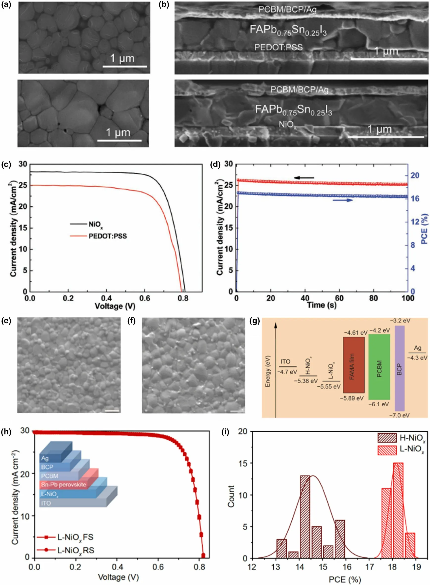
Figure 8. a) Surface SEM images of FAPb0.75Sn0.25I3 perovskite films fabricated on PEDOT:PSS HTL (top) and NiOx HTL (bottom) and b) resulting PSC device cross section with PEDOT:PSS HTL (top) and NiOx HTL (bottom). c) J-V characteristics of resulting PSCs and d) champion device steady-state photocurrent and PCE at a constant 0.650 V bias. Reproduced with permission.[8] Copyright © 2018, Wiley. e) Surface SEM images of MA0.4FA0.6Pb0.4Sn0.6I3 perovskite films fabricated on H-NiOx and f) L-NiOx HTL films. g) Energy-level diagram for the PSC device containing H-NiOx and L-NiOx HTLs. h) Forward and reverse J-V characteristics of champion PSC containing L-NiOx with the device schematic in the inset and i) PCE comparison of the two types of devices. Reproduced with permission.[95] Copyright © 2020, Springer Nature.

Figure 9. a) The ABX3 structure of metal halide perovskite made of BX6 octahedra and AX3 sublattice(cubic close packed). b) Perovskite lattice with possible A, B, and X ions with varying ionic radii.Schematic diagrams depicting the bandgap tuning of Pb-only and Sn-incorporated metal halide perovskites by altering A, B, or X sites; c) single and double A-cation perovskites with MA, FA, and/or Cs.Reproduced with permission.[190] Copyright © 2017, Elsevier. d) Single A-cation perovskites with FA or MA. Reproduced with permission.[191] Copyright © 2014, Wiley.
In metal halide perovskites for PSCs, using a combination of different cations such as FA+and MA+in the A-site is preferred over single cation systems, due to the complementary qualities brought together to the absorber layer (such as higher thermal stability from FA+and higher structural stability from MA+).[102]These multication systems were initially synthesized for Pb-only perovskites and have since been adopted for Pb-Sn mixed PSCs. Thus, they can be best understood by briefly reviewing Pb-only systems first. For instance, higher structural stability in FAPbI3was reported when the formula was altered to FAxMA1-xPbI3through MA+incorporation, MA+forms string interactions with the PbI6octahedra,thereby stabilizing FAPbI3against degradation into its photoinactive δ-FAPbI3(yellow)phase.[103]In turn,FA+provides excellent thermal stability for the perovskite at temperatures over 165°C (that MAPbI3alone cannot achieve), through bonding strongly with I−in the lattice.[102,103]However, FA+brings moisture sensitivity to the perovskite due to its higher hygroscopic nature,[102]and efforts have been made to provide stability against humidity by further incorporation of Cs+with FA+or MA+in the perovskites.As such,CsxMA1-xPbI3or CsxFA1-xPbI3was reported to have considerably higher stability against humidity with contrast to the MAPbI3or FAPbI3,[104]while for MA+-containing perovskites,Cs+also contributed to thermal stability ~120 °C[104,105]and gave rise to highly cubic perovskites(0.9 ≤t ≤1) when in FA+-based ones.[105]Due to these enhancements, Cs+also enables less stringent conditions during the perovskite fabrication process.[106]In order to combine the desirable qualities of all three cations discussed above,a triple cation perovskite formula was introduced next for Pb-only PSCs, in which the photoinactive δ-FAPbI3phase was entirely inhibited by Cs+, while more grain growth was facilitated.[106]With a more cubic structure, multication mixtures are regarded more stable,which has been proven by the triple cation perovskites showing remarkable high efficiencies and stabilities in Pb-PSCs.[106,107]With these fundamentals in mind, similar research on Pb-Sn perovskite absorbers is discussed in the following subsections. In Pb-only PSCs, incorporation of Rb+, K+, Na+etc.[108]was also reported to aid in defect passivation and stability; however,these cations have yet to be explored for Pb-Sn mixed perovskites.
3.2.2. Single A-Cation Pb-Sn Mixed Perovskites
Similar to MAPbI3in Pb-PSCs, MAPb1-xSnxI3(0 ≤x ≤1) is the widely studied in Pb-Sn PSCs, especially during the early stages. In 2014, MASn0.5Pb0.5I3was used in a standard n-i-p device structure with mesoporous TiO2ETL, which resulted in 4.18% PCE.[23]Within the same year, the Jen group employed a planar inverted (p-in) architecture with a MAPb0.85Sn0.15I3absorber yielding a higher PCE of 10.1%.[12]The same group then employed PEDOT:PSS as HTL and fullerene derivatives as ETL in Pb-Sn mixed PSCs for first time,in the same year, to fabricate a ITO/PEDOT:PSS/MAPb1-xSnxI3/PCBM/bis-C60/
Ag stack, concluding that the p-i-n configuration is better suited for Pb-Sn mixed systems.[12]With I−as the halide, various x values in MAPb1-xSnxI3give rise to different crystal structures and in different PCEs[11]with the highest PCE of 15.85% (for x = 0.6).[38]However, in 2017,the efficiency of MA-only Pb-Sn PSCs was improved up to 17.63%by substituting 20% of the halide site with Br−resulting in a MAPb0.5Sn0.5(I0.8Br0.2)3formula.[9]So far, for the “standard” device architecture with MAPb1-xSnxI3absorber, a highest PCE of 15.5%has been reported.[91]
High efficiencies are also seen with single cation FA-only Pb-Sn mixed PSCs(although not as widely reported as MA-only ones),where a highest PCE of 17.25% was reported for a device with a ITO/NiOx/FAPb0.75Sn0.25I3/PCBM/bis-C60/Ag stack,[8]and bandgap of 1.36 eV,very close to the ideal value for a single-junction solar cell defined by the Shockley–Queisser limit (1.35eV).[68,109]Furthermore, in Pb-Sn mixed perovskites, a small amount of Sn2+was found to aid stabilization of the FAPbI3α-phase (preventing the photoinactive δ-FAPbI3phase; much like incorporation of MA+and Cs+), without the aid of any other A-site cation.[110]Reportedly, Sn incorporation further reduces the temperature necessary for the δ-phase to α-phase conversion,to around 100°C, which otherwise lies in the range of ~125 °C– 60 °C.[102]In this study, high crystallinity and robustness wereachieved for a FAPb0.5Sn0.5I3absorber, as a result of the higher structural stability.

Table 1. Reported work on Pb-Sn Mixed planar inverted PSCs up to date. The results are listed in the order of increasing Sn content
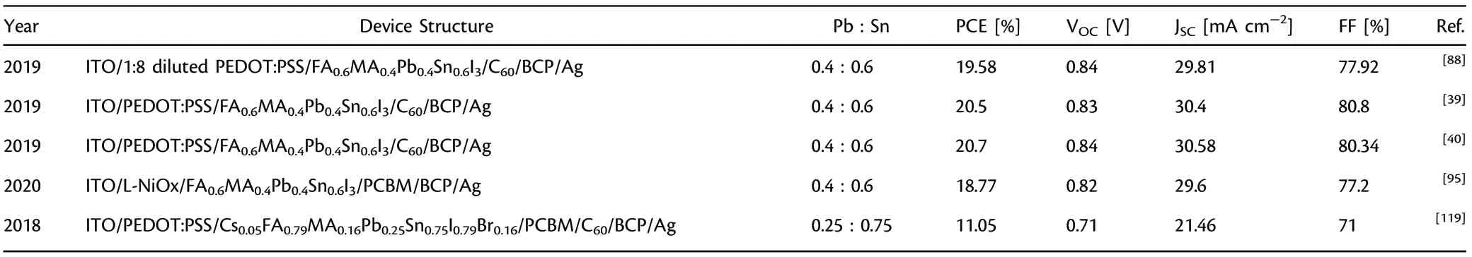
Table 1. Continued
The single cation systems discussed so far involve organic A sites,to fabricate inorganic–organic mixed perovskites. However, in Pb-Sn mixed PSCs, experimental reports on “all-inorganic” perovskites with Cs+as the single A-cation is not widely reported for PV applications.This is mostly due to implications of bandgap energies and phase stabilization issues. A study by Cao et al. reported a CsPb1-xSnxI3perovskite with x = 0.5 to absorb a wavelength of 900 nm NIR-I radiation.[111]This result is in par with a recent theoretical study by Valadares et al.,[112]on CsPb1-xSnxI3perovskites where most mixed compositions showed bandgap under 1.2 eV with the lowest of 0.984 eV (for x = 0.8). Thus, the all-inorganic Pb-Sn mixed perovskites with I−as halide may qualify for absorbing higher wavelengths of the solar spectrum; however, their Pb-only and Sn-only counterparts have reported much lower efficiencies for CsPbI3(majority of reports with PCE~15%with highest of 18%)[113]and CsSnI3(maximum PCE reported 5.03%despite the ideal bandgap of~1.3 eV and theoretical PCE of 30%),[114]compared with their inorganic–organic mixed analogues. For CsPbX3,the problem lies in larger bandgaps and unfavorable band alignments,as well as phase stabilization issues with the small Cs+cation radius.[113]In contrast, the smaller Sn2+ion in CsSnX3is better equipped to accommodate Cs+in the perovskite lattice,with a tolerance factor closer to 1.[115]However, the poor interfacial and film qualities(which increase Sn2+oxidation and non-radiative recombination), as well as phase stabilization issues under ambient conditions,have led to their low performance as well.[114]These limitations could be the primary reason for the lack of CsPb1-xSnxI3compositions utilized for narrow-bandgap photovoltaic devices. However, as reported by Valadares et al.[112]in their theoretical simulations, CsPb1-xSnxI3perovskites with atomic arrangements less susceptible to oxidation can be formed through low-temperature fabrication methods. As discussed in the previous section, in inorganic–organic mixed perovskites, incorporating Cs+is directly linked with improved stability of the absorber films. Similarly, all-inorganic Pb-Sn mixed perovskites with a mixed IBr halide composition (I:Br = 1:2) commonly report increased device stabilities under ambient conditions (although higher bandgap >1.6 eV Br-rich perovskites are more suitable for wide-bandgap PSCs).[22,116]Liang et al. studied a CsPb1-xSnxIBr2with (x = 0.1 and bandgap 1.79 eV) fabricated under ambient conditions without a glovebox or a thermal evaporator.[22]The authors reported a highly reproducible,stable,heat,and moisture resilient PSCs with a champion efficiency of 11.33%and a high VOCof 1.27 eV,with the potential for low-cost batch production.Li et al.studied the same perovskite composition with x = 0, 0.25, 0.5, and 0.75, which showed bandgap tunability from 2.04 eV to 1.64 eV with increasing Sn.[116]For x = 0.25,a PCE of 11.53%with VOC= 1.21 V was achieved with a better stability under illumination than its Pb-only counterpart.A recent theoretical study by Schwartz et al.on fully Br−containing CsPb1-xSnxBr3compositions reported that the bandgap can be tuned 1.86(x = 1)to 2.37 eV(x = 0)for applications in wide-bandgap PSCs or light-emitting diodes(LEDs).[117]More evidence is needed to realize fully inorganic Pb-Sn perovskites for PV applications.
3.2.3. Double A-Cation Pb-Sn Mixed Perovskites
Much like Pb-only PSCs, double cation systems have also been studied for Pb-Sn PSCs. Here, the perovskite precursor takes the form of FA1-yMAyPb1-xSnxI3, and to date, much of the higher efficiencies(>20%) for Pb-Sn mixed PSCs has been reported commonly with x = 0.5–0.6 and y = 0.3–0.5 (see Table 1). Over 20% efficiencies were first reported in 2019[34,39,40]and higher efficiencies were continuously achieved[12,43,44](currently over 21%) with FAMA double cation system (recently addressing the surface passivation aspect more,to improve stability and PCE). Beyond the benefits of FA, MA mixed perovskites discussed for Pb-only PSCs above,the FA-MA mix in Pb-Sn mixed perovskites also aid in slower oxidation of Sn2+,[12]whilst enabling better quality films with uniform surface coverage. However,FA-based Pb-Sn perovskites are still sensitive to humidity, which may be a primary reason that surface passivation techniques provide prominent efficiency improvements in FA1-yMAyPb1-xSnxI3PSCs.Many of the reported high efficiencies were obtained by incorporating such passivation methods and other additives, which will be discussed in depth in Section 3.4.
Similar to Pb-only PSCs, the field of Pb-Sn mixed perovskites has explored the incorporation of Cs+in the crystal lattice as a remedy for humidity issues.[32]In a study by Beal et al.,MAPb0.5Sn0.5I3perovskites with 10% Cs+inclusion reportedly improved the stability of the PV devices.[26]With an initial PCE of 10.07%(compared to 6.36%of PSC without Cs+),the champion device retained 76%of its initial PCE after 20 days in dark, ambient conditions with 35% humidity, becoming the first stable Pb-Sn PSC under ambient condition storage.The authors reported a slower crystallization rate improving the homogeneity of film morphology upon Cs+incorporation, with uniform grains, and lower Sn2+oxidation through lattice contraction achieved by its small ionic radius.[26]The authors also note that too much of Cs+results in phase separation in the perovskite, necessitating the Cs+content to be properly optimized. Furthermore, when the Pb content was increased to 75% in the B-site (Cs0.1MA0.9Pb0.75Sn0.25I3), a PCE of 14.55% was obtained in this study.
In FA-based Pb-Sn perovskites, Cs+incorporation (from 20% to 30% of the A-site reported in various occasions) has resulted in higher device stability against humidity, temperature, and illumination.[1,118]FA-Cs combination is much often reported in Pb-Sn mixed perovskites than MA-Cs mixture, and much higher efficiencies have also been reported. Notably, for a (CsSnI3)0.3(FAPbI3)0.6formula, a 15.8% PCE was achieved by Zong et al. after incorporating a SnF2∙ 3FACl Lewis-base adduct in the precursor solution,[118]through passivating the grain boundaries with SnF2(released following the evaporation of FACl during annealing), which accumulates at the grain boundaries. A remarkable retention of 90% of its initial PCE was reported for this device after 288 h in ambient air. In recent reports, much higher PCE of > 20% (at maximum power point) was achieved with a Cs0.25FA0.75Pb0.5Sn0.5I3absorber, through a gas quenching process to replace anti-solvents in perovskite crystallization.[42]In this study, the PEDOT:PSS HTL was also replaced with PTAA, and the authors reported a high thermal stability of the cells with 80% original PCE retained after 4000 h at 85% °C, and fairly large are cells (1 cm2) were fabricated with 17.5% PCE.
3.2.4. Triple A-Cation Pb-Sn Mixed Perovskites
Unlike their Pb-only counterparts, only a limited number of triple Acation systems are reported for Pb-Sn PSCs. One such Pb-Sn mixed triple cation, mixed halide system by Ji et al. utilized a Cs0.05FA0.79-MA0.16Pb0.664Sn0.336I2.48Br0.52perovskite,[37]following the A and X compositions reported for highly stable Pb-only PSCs.[106]The authors fine-tuned the bandgap with a Sn2+stoichiometry of 0.336 to achieve a higher stability and a PCE of 16% PCE which retained 93% of its initial PCE for 30 days.[37]In other work, Bandara et al. reported a Cs0.05(FA0.83MA0.17)0.95Pb0.5Sn0.5I3formula with 50% Sn2+content(and I−only), resulting in 12.04% PCE.[47]Here, the authors employed toluene as the anti-solvent and a surface wash, to remove the Sn4+dopants in the absorber. The same group later reported surface passivation with guanidinium bromide (GABr), improving the PCE up to 14.4% and reported ~83% FF, the highest reported fill factor for Pb-Sn mixed PSCs.[7]The authors found that in addition to the surface passivation, the perovskite was doped with Br−across the thickness, which gave rise to better electronic properties in the PSC.An important parameter for Pb-Sn mixed triple cation perovskites, the effect of Cs+, was studied by Tosado et al. Csx(FA0.83MA0.17)1-xPb1-ySny(I0.83Br0.17)3with x = 0.05, 0.10, 0.20 and y = 0, 0.25,0.50,0.75,1.0.[119]Combining various x:y contents,the authors studied 15 different compositions for perovskite absorber grain morphologies, observing that the grain size was more correlated to the Sn2+content than the Cs+content. However, it was noted that for larger Sn2+contents(>75%),lower Cs+content was preferred for a pinholefree layer with large grains. Incorporation of Cs+pushed the Goldschmidt tolerance factor of these perovskites more into the cubic region further away from hexagonal (gradually from x = 0 to x = 0.2), aiding the stabilization of the perovskite against phase changes.Moreover,suppressing the yellow phase and the oxidation of Sn2+,the Cs+incorporation was reported to give rise to highly crystalline perovskite films,and the authors fabricated 75% Sn-containing Pb-Sn mixed PSC with 11.05%PCE with x = 0.05(such studies with>60%Sn incorporation is not widely reported in Pb-Sn mixed PSCs yet). Best performance for 50%Sn and 25%Sn was achieved with x = 0.1 with champion PCE of 13.52% and 15.78%, respectively. The devices retained ~80% initial efficiency after 30 days under inert atmosphere.[119]More recently, Li et al. achieved 20.4% PCE for a Cs0.05FA0.85MA0.10Pb0.5Sn0.5I3triple cation absorber.[41]Here,a 2-step fabrication method for the perovskite film as well as a 1D perovskite to passivate the surface was employed to achieve the high performance, which will be discussed in depth in Section 3.4.3 of this review. However, the authors highlighted the importance of reduced MA content (only 10% of A-site) in reaching high stability in the devices,retaining 92%of initial PCE after continuous operation under 1 sun for 450 h.
3.2.5. Engineering B and X sites of Pb-Sn Mixed Perovskites
As noted in Section 3.1, the B and X site molecular orbitals directly generate the VBmaxand CBminof the metal halide perovskite,thus altering B and X ions directly tunes the bandgap.[99,100]As discussed so far,the most common strategy for B-site tuning is Sn2+substitution to completely or partially replace Pb2+(Figure 10a-c),[98]the bandgap shows a “bowing effect” with increasing Sn at via B-site and will be discussed later in this section. When engineering the X site halide to alter the bandgap,among available halides,Br−incorporation in I−only perovskites has been widely acknowledged to increases the bandgap(Figure 10d,e),[32]where the Br−concentration was reported to directly correlate with the bandgap increment in Pb-only perovskites,following a quadratic relationship.[32]Furthermore, it improves crystallinity, increases grain sizes, and passivates defects while enhancing charge extraction, reducing disorder and hysteresis, and providing ambient stability.[9]
In Pb-Sn mixed PSCs, the partial substitution of Pb2+with smaller Sn2+ions was reported to alleviate phase segregation in mixed I-Brcontaining absorbers. In a study by Yang et al., a MAPb0.75Sn0.25(I0.6Br0.4)3composition was studied with respect to its Pb-only counterpart.[27]Reportedly, the Pb-Sn mixed PSCs, phase segregation under illumination was eliminated, attributed to the alterations in the internal bonding environment(crystallite size and micro-strain) resulting from Sn2+substitution. Next, bandgap tuning of this composition was explored by varying the Br composition at the x site of the MAPb0.75Sn0.25(I1-yBry)3absorber(Figure 10d).Increasing Br from 0%to 100% resulted in gradual bandgap widening of the resulting absorbers as observed by the linear shift of the optical absorption onset from 1.35eV(MAPb0.75Sn0.25I3)to 2.03 eV(MAPb0.75Sn0.25Br3).Increments of VOCand FF of resulting PSC devices were reported with increasing Br−up to 60-70% (Br content) which decreased for higher Br−contents,whereas JSCwas reported to gradually decrease with increasing Br from 0% to 100%. Furthermore, all I-Br compositions showed single phase perovskites with pseudo cubic unit cell structure, with gradual lattice contraction observed for increasing Br content. The authors selected I:Br as 0.4:0.6 as the best composition with a 1.73 eV bandgap for wide-bandgap cells, with a resulting 12.59% PCE (VOC1.04 V, JSCof 15.52 mA cm−2, FF 78%) for a ITO/PEDOT:PSS/MAPb0.75Sn0.25(I0.4Br0.6)3/PC61BM/bis-C60/Ag PSC device.
A later study by the same authors reported improvements in a MAPb0.5Sn0.5(I0.8Br0.2)3composition compared to a MAPb0.75Sn0.25I3reference absorber.[9]The authors reported lower band edge disorder in the Br containing composition along with higher quasi fermi level splitting, higher crystallinity, and better film morphology, significantly improving the optoelectronic qualities of the new absorber. However,the changes were attributed to the alterations in both B and X sites in this study and not Br incorporation alone.The bandgap of the new absorber decreased to 1.35 eV from 1.39 eV of the reference.This can be attributed to the 25%increment of Sn2+in the B site,which seemingly compensated for the bandgap increment that should have resulted from 20%increment of Br−in the X site.Here,both the CBminand VBmaxof the Br−containing absorber were reported to shift down by 0.12 eV,providing better energy-level alignments with the charge transporting layers of the PSC devices fabricated. Compared to the 12.09% PCE of the reference, an improved 14.71% PCE was observed for the improved absorber, which was further improved to 17.13% by increasing the thickness of the absorber. In another study, a triple cation Cs0.05FA0.79MA0.16Pb1-xSnxI2.48Br0.52was employed to achieve Pb-Sn mixed PSCs with champion PCE up to 16.10% with good stability and negligible hysteresis.[37]A comparison with a Pb-only counterpart was not discussed in this study, and the authors seem to have adopted the formula directly from triple cation mixed halide Pb-only perovskites given their popularity in highly stable and efficient PSCs.[37]In a similar study for a Cs0.05FA0.79MA0.16Pb0.5Sn0.5I3perovskite, Br−was incorporated as post-treatment on the original Icontaining perovskite film.[7]Here, the authors have employed a GABr (guanidinium bromide) treatment as a surface passivation layer for the absorber, which resulted in a distribution of Br−ions through the bulk of the perovskite film, with a final film composition of Cs0.05FA0.79MA0.16Pb0.5Sn0.5I0.24Br0.6. An increment of the PCE from 12.2% (I−only PSC) to 14.4% with high fill factors of 83% (Br−incorporated devices) was reported in this study. Similar to previous reports, the bandgap increased from 1.25 eV to 1.30 eV with Br- incorporation, while the CBminand VBmaxwere shifted downwards by 0.1 eV with respect to the reference energy levels.The authors also reported a shift in Fermi energy of the Br−incorporated absorber by 0.1 eV upwards (with respect to the reference perovskite Fermi level) toward CB edge, signifying that the Br−incorporation also contributes toward n-doping of the perovskite film. This can especially be beneficial for Pb-Sn mixed perovskites in compensating for loses due to Sn2+oxidation, thus should be further explored in Sn-containing PSCs. A remarkable PCE of 19.03% was achieved by Li et al. for FA0.6MA0.4Pb0.4Sn0.6(I1-xBrx)3composition with x = 0.06 compared to the 17.03% of I−only reference.[120]The surface recombination was reported to reduce thorough this route, with the defect density being reduced from 1017to 1015cm−3. Br−incorporation was found to aid in passivating the grain boundaries which contribute largely to the leakage currents of the Pb-Sn mixed PSCs.[120]
For Pb-based PSCs, Cl−incorporation at the X site has also been reported in some instances. However, the effect of it is not very well understood, despite the improved film morphology and slow crystallization rate reported.[121]Similarly,Cl−incorporation can be seen in a limited number of Pb-Sn mixed PSC studies.[12,82]In one of the first reported studies on Pb-Sn mixed PSCs by Zuo et al,[12]a Cl−containing MAPb1–xSnxI3−yClyperovskite was explored in comparison with its Pbonly counterpart MAPbI3−yCly. A PCE of 10.1% was reported for the Pb-Sn mixed PSCs with 15% Sn incorporation in the above formula,compared to a 7.3% of the Pb-only PSC for inverted devices. The authors report a steady loss of Cl−in both Pb-only and Pb-Sn perovskites during the fabrication process and attributed it to a similar process as the mechanism of iodide loss in pure organo-lead iodide perovskites (via decomposition of MAI). The authors suggested that MACl was decomposed into methylamine (CH2NH2) and HCl gases,during the film annealing process. In addition, a separate Cl−containing MAPb1-xSnxCl3phase was observed in both perovskites under XRD,with a strong suppression of this phase with Sn substitution. The authors reported the formation of Sn-Cl bonds before the other bonds in the system,indicating the influence of the presence of Sn in Cl−containing perovskites. This rapid formation of Sn–Cl was observed to complicate the growth and resultant morphology of Pb-Sn mixed perovskites,limiting the degree of Sn substitution.Furthermore,in contrast to the Br−containing perovskites, the unit cell structure for MAPb0.85Sn0.15I3-yClywas found to be tetragonal (similar to MAPbI3-yCly),[12]where Br−-containing Pb-Sn mixed perovskites are often reported to be cubic.[27]However,the authors emphasized the need for more research toward understanding the function of Cl−in enhancing the ultimate material properties of perovskites. In another Pb-Sn mixed study by Liu et al, Cl−-incorporated MASn0.5Pb0.5IxCl3-xformula was reported to result in high-quality film morphology and low bandgap,with an optical absorption edge exceeding 1000 nm.[82]Similar to the previous study by Zuo et al,[12]the Cl−content here was reported to reduce during the perovskite film fabrication process; however, the authors suggested the loss mechanism as sublimation of MACl.[82]Here, an accelerated MACl sublimation was reported to result in films with better film coverage,crystallinity,and reduced trap density,which was achieved by a vacuum-assisted thermal annealing process. However, the authors reported a resulting composition of MASn0.5Pb0.5I3where negligible amounts of Cl−were observed in the film.Moreover,incomplete sublimation of MACl resulting from annealing the film in non-vacuum environments was reported to adversely affect the perovskite, acting as an impurity. Thus, the functionality of Cl−for the perovskite functionality is not very clear in this study as well. In later reports,high efficiency up to 18.4%was reported with 2.5%Cl−incorporation in a FA0.6MA0.4Pb0.4Sn0.6(I1-xClx)3perovskite by Zhao et al.[122]The improvements were attributed to increased grain sizes,better crystallinity,grain boundary passivation,high charge carrier lifetimes, and high carrier mobilities. So far, majority of the Pb-Sn PSCs seem to prefer I-only compositions over mixed halides.However,considering the above results, mixed halide systems are another viable pathway for future exploration in Pb-Sn mixed systems en route to achieving higher PCE.
Considering the B-site, as noted earlier in this section, when tuning bandgap (1.2 – 1.3 eV) by altering Pb2+:Sn2+ratio, the bandgap variation shows a “bowing effect” with increasing Sn2+content,defying Vergard’s law (Figure 11a).[10]Here, a decrement of the bandgap is initially seen with increasing Sn content, reaching a minimum at ~40% - 60% Sn2+(the perovskite formula decides the exact Sn content to achieve the minimum bandgap) which then increases when Sn2+content is further increased.[10]This bowing effect can be described using Equation 3 below, where Egis the bandgap energy and b is the bowing parameter. This describes how strong the bandgap bowing is.

With the bandgap, both VBmaxand CBminwere observed to shift,and the reasoning for the bowing effect is still under debate(Figure 11b).[10]Shift toward lower energies (higher wavelengths) of absorption edges in EQE(also known as IPCE,incident photon conversion efficiency) and optical absorption spectra (Figure 11c and d), as well as the PL emission peaks,[68,123]was seen with Sn incorporation of up to 50%which then show opposite shifts upon reaching 100 Sn%.
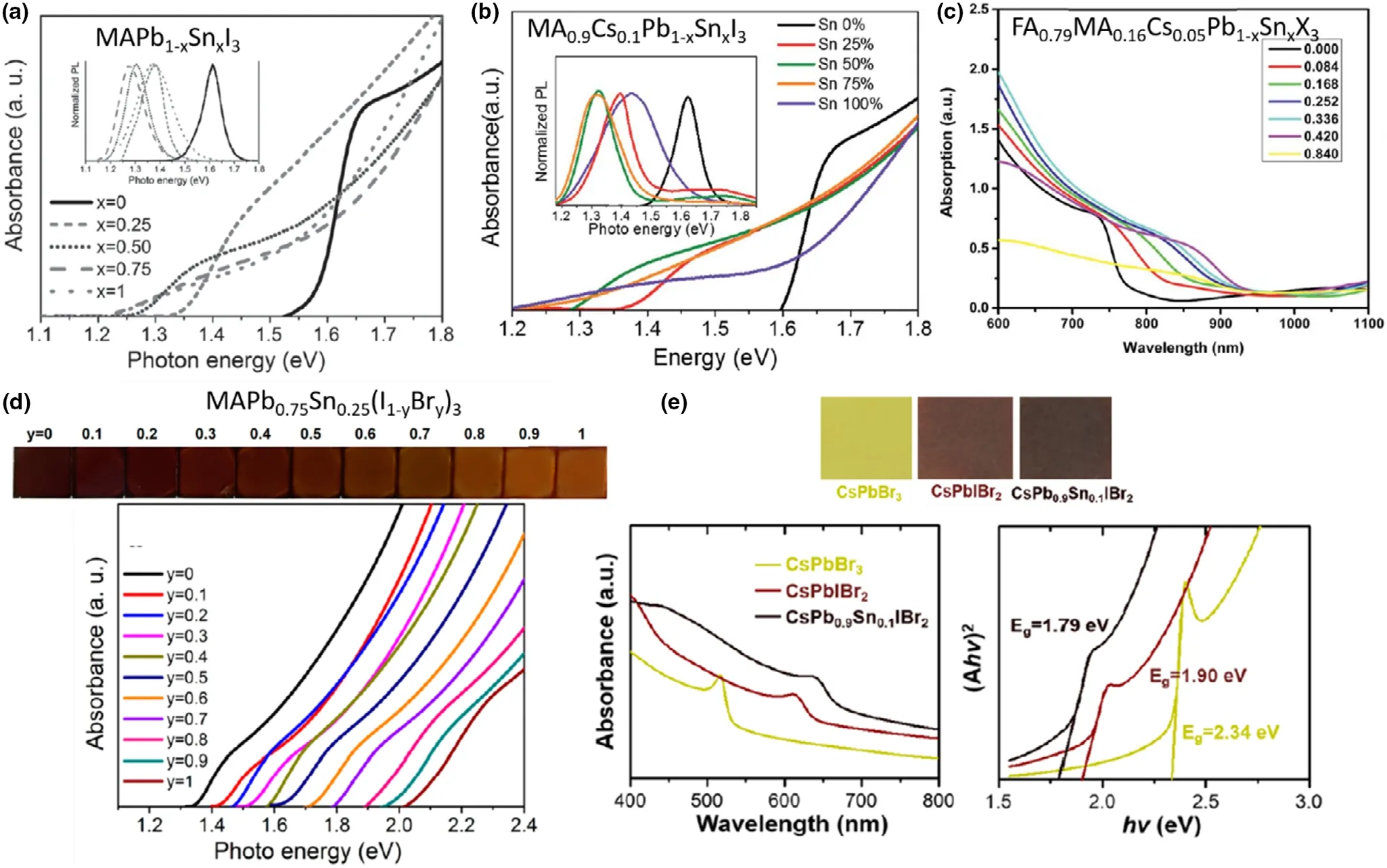
Figure 10. Bandgap tuning of Pb- and Sn-containing perovskites seen from optical absorption edge and/or PL peak shifts, with varying Sn content in a)single cation MAPb1-xSnxI3, Reproduced with permission.[11] Copyright © 2016, Wiley. b) Double cation MA0.9Cs0.1Pb1-xSnxI3 Reproduced with permission.[26]Copyright © 2016, Royal Society of Chemistry and c) triple cation FA0.79MA0.16Cs0.05Pb1-xSnxX3 perovskites. Reproduced with permission.[37] Copyright ©2019, Royal Society of Chemistry. Bandgap tuning via halide ion substitution by d) tuning the Br content in MAPb0.75Sn0.25(I1-yBry)3. Reproduced with permission.[27] Copyright © 2016, American Chemical Society and e) tuning both halide and Sn content in all-inorganic CsPb1-xSnxI1-yBry perovskites.Reproduced with permission.[22] Copyright © 2017, American Chemical Society.
There are several hypotheses that attempt to explain bandgap bowing, such as spin-orbit coupling and lattice distortion with Sn2+incorporation,[124]short range ordering of Pb-Sn atoms,[1]deeper conduction band edge of MASnI3and shallower valence band edge of MAPbI3,[125]and the energy mismatch of Pb2+and Sn2+atomic orbitals.[123]In Pb-only perovskites such as MAPbI3, atomic orbitals of Pb(B site) and I (X site) give rise to the band structure.[99]Here, Pb(6s)and I(5p) orbitals contribute to the VBmaxthrough σ-antibonding interactions, while the CBminis made from a mixture of σantibonding molecular orbitals from Pb(6p) and I(5s) and πantibonding molecular orbitals from Pb(6p) and I(5p).[99]It is generally accepted that the band structure and bandgap of Sn-based perovskites originate in a similar manner through Sn and I atomic orbitals.[123]However, ab initio calculations at DFT, hybrid DFT,and QSGW levels of theory have shown, via analysis of the partial density of states (PDOS) (Figure 11e),[123]that the atomic orbitals of Sn (right) reside at more shallower energy levels than Pb orbitals (left), resulting in more shallower VBmaxand CBminenergy levels for Sn. Thus, for a mixed Pb-Sn system (Figure 11e (middle)), the orbital diagram would show a CBminmade of Pb-I orbitals and a VBmaxmade of Sn-I orbitals which gives rise to the anomalous bandgap with a bowing parameter of 1.08 eV. This research also suggests that the bowing effect is related primarily to the energy mismatch between the Pb 6s/6p and the Sn 5s/5p states, suggesting that spin-orbit coupling and the short range ordering are not the primary cause of the bowing. Calculations which include and exclude spin-orbit coupling found very similar bowing parameters, although the linear term of the bandgap as a function of Sn content is strongly affected due to the lower atomic number of Sn relative to Pb. The short range ordering of Pb and Sn atoms is considered to not influence the bandgap bowing, as random distributions of Pb and Sn atoms were shown to result in a lower total energy than clustered distributions of Pb and Sn atoms, suggesting that the formation of Pb and Sn clusters is not preferred. The results of this research also show that lower levels of theory, such as GGA level functionals, describe the behavior of the band edges and bandgap bowing well, which is useful for keeping calculation of the large systems needed for these solid solution calculations affordable.
The role of X site atomic orbitals in band edge formation explains how the bandgap can be tuned via halide ions, as discussed above. In Section 3.1, it was also noted that the A-site can indirectly affect the bandgap. This can happen as a result of either perovskite lattice contraction or tilting of BX6octahedra.[3]For instance, it was reported that incorporating Cs+in FA-based Pb-Sn perovskites rich in Pb increases the bandgap via octahedral tilting, and when rich in Sn, this decreased the bandgaps through lattice contraction.[3]In pure Pb-based FA1-xCsxPbI3, DFT calculations have shown that the bandgap increases with increasing Cs+content, as the small ionic radius of Cs+induces a lattice contraction. Due to the relatively large size of Pb2+, and the size mismatch between FA+and Cs+, this causes a lowering of the crystal symmetry from the cubic to tetragonal phase, which causes a decreased orbital overlap of Pb2+and I−in the band edges, causing a lower band dispersion, and thus an increased bandgap.[126,127]
3.3. Fabrication of Absorber Layers
In Pb-Sn PSCs, the absorber layer is a thin film of a few hundred nanometres, and the fabrication of very high-quality film tuning its structure and morphology has been continuously regarded as the primary path in achieving highly efficient and stable PSCs.[63,128]In other words,a highly crystalline,pinhole free,smooth film with large grains is desirable, which can generally be tuned via the selection of suitable fabrication methods, processing conditions, surface post-treatments,compositional engineering, etc.[128,129]These parameters are interdependent, and the perovskites (especially Sn-incorporated ones) are highly sensitive to small alterations in them,which makes it difficult to independently identify the impacts of each factor on the reported changes in most cases.[63]
Figure 11. Anomalous bandgap behavior (bowing effect) of Pb-Sn mixed perovskites as seen by a) plot of energy gap Vs. fraction of Pb, b) schematic diagram showing the CB and VB levels and corresponding bandgap values, c) absorption edge shift as seen in IPCE spectrum, and d) absorption edge shift in an optical absorption spectrum; for a MAPbxSn1-xI3 formula with x = 1, 0.75, 0.5, 0.25 and 0. Reproduced with permission.[10] Copyright © 2014, American Chemical Society. e) Schematic representation of the origin of the bandgap bowing in MAPbxSn1-xI3. Shaded regions represent the valence and conduction bands with white gap in the middle representing the bandgap energy, Eg. Reproduced with permission.[123] Copyright © 2018, American Chemical Society.
3.3.1. Fabrication Methods
The perovskite film can be fabricated through a solution-based deposition or vacuum deposition,[129]the former being most widely reported with the lower cost associated and ease of adoption in commercial scale. In laboratory scale, spin coating is commonly used, where the perovskite precursors are dissolved in a suitable solvent/solvent mix and deposited either through one-step deposition, or multi-step (sequential)deposition.[129]Although the one-step process is straight forward, cost-effective, and more suited for planar device architectures compared to sequential deposition, the latter provides better morphological and crystallization control and is less prone to pinhole formation.In one report employing sequential deposition,a two-step bilayer interdiffusion growth process (BIG process)was employed by Li et al,[41]to produce very high-qualityCs0.05MA0.1FA0.83Pb0.5Sn0.5I3absorbers (Figure 12a-e) with large grains and reduced amount of volatile MA.However,this processing route requires additional annealing steps to either aid crystallization,merge the precursor layers, or remove excess solvent accumulation as well as controlled atmospheric conditions in order to aid proper crystallization.[129]To achieve better control in a one-step deposition process,the precursor solution has to be carefully fine-tuned considering the solvent system,as well as the precursorconcentrationandratios.[63,129]Considering fabrication methods, when it comes to the large area manufacturing of PSCs the spin coating method has limitations. As a resolution to this,another method of solution deposition, blade coating, was recently adapted for a Pb-Sn mixed perovskite by Li et al.[130]This method was developed as means of fabricating high-quality large area perovskite films,where the precursor solution was coated in a one-step process and subjected to both vacuum and thermal annealing (Figure 12f).[130,131]The authors fabricated Pb-Sn mixed PSCs with 1 cm2active area using this method.[130]Also, this method was used by the authors for producing for Pb-only perovskite solar modules with 10.08 cm2active areas (4 cells connected in series).[131]More large area methods such as these need to be further explored for Pb-Sn mixed PSCs.
The next type of fabrication is vacuum deposition of precursors. Although this method fabricates highly uniform and crystalline perovskite films,[132]the evaporation rate must be heavily controlled for each precursor/precursor mixture to achieve a stable stoichiometry throughout the films.In some cases, vacuum techniques are used in sequence with solution processing, where a vacuum deposited film of the first precursor is exposed to the vapor of the second precursor allowing better control of the diffusion of the two precursors.[133]Although vacuum techniques are not suited for lowcost applications, they have been investigated for perovskite-Si tandem devices. There are many other factors affecting the quality and optoelectronic properties of perovskite thin films, including the environmental conditions during fabrication (air exposure, humidity, etc.), annealing conditions (temperature, time, controlled solvent annealing, etc.), as well as solvents and additives.[63]These are of higher importance in Pb-Sn and Sn-incorporated perovskites with higher reactivity (as discussed in the following sections), thus must be properly engineered.
3.3.2. Environmental Conditions
Most perovskites are fabricated in an inert environment due to their air and moisture sensitivity (mostly due to FA+).[128,129]However, this is even more critical in Sn-containing perovskites,due to the rapid oxidation of Sn2+to Sn4+upon exposure to atmosphere.[64]Interestingly,in come Cl−containing Pb-only perovskites,film fabrication under~30%humidity was reported to give rise to higher efficiencies through the formation of larger grains,and achieving full,pinhole-free surface coverage.[134]However, Pb-Sn perovskites still suffer rapid oxidation of Sn2+to Sn4+even when processed under N2glove box with carefully controlled moisture levels. Very recent reports have provided viable methods to tackle this,such as the incorporation of metallic Sn powder in Pb-Sn mixed perovskites (further discussed in Section 3.4.2).[45]However, in the future it is best to employ proper encapsulation and surface passivation of the Pb-Sn mixed PSCs,to protect the films against ambient moisture and air.
3.3.3. Solvent and Additive Engineering
In solution-processed perovskites, the solvent system must be well engineered to allow compact,pinhole-free,highly crystalline,and morphologically controlled perovskite films. The most widely used solvent systems for Pb-Sn mixed perovskite precursor solutions contain a mixture of polar aprotic solvents DMF (N,N-dimethylformamide) and DMSO (dimethyl sulfoxide).[129]DMSO in the solvent system reportedly allows controlled and complete conversion of PbI2into the perovskite film by formation of PbI2-DMSO adducts, while when DMF was used alone, PbI2crystallization lacks control.[135]Similarly, SnI2-DMSO complexes adducts were reported for Sn-based perovskites as well.[29,136]Although these solvent systems aid in bypassing the limitations for homogenous nucleation in one-step fabrication processes,[129]the toxicity of these solvents limits their usage in large-scale commercial applications, while recent reports in Sn-only perovskites also suggest that DMSO can contribute to Sn2+oxidation.[137]Therefore, testing more suitable solvent systems is highly important for Pb-Sn perovskites at present.
Another popular technique for high-quality perovskites is the “antisolvent treatment”,[138]which is commonly used in high-performing PSCs.[139]This technique bypasses the limitations of extremely slow solvent evaporation rates and facilitates fast crystallization of perovskites.[129]The anti-solvent is selected such that it is well miscible with the solvents but does not take part in dissolving the perovskite or its precursors.During the spin coating,the anti-solvent is dripped on to the film to cause instantaneous local supersaturation.[138]This in turn gives rise to the fast heterogeneous nucleation process. Inspired by the Pb-only PSC fabrication methods, several different anti-solvents have been explored for Pb-Sn mixed perovskites(Figure 13a).Among these,the most common are toluene,[11,28]anisole,[1,13]chlorobenzene,[17,88]and diethyl ether,[122,140]while less commonly, other anti-solvents such as ethyl acetate[34]and o-xylene[91]have also been tested for Pb-Sn mixed PSCs. Although the effect of different anti-solvents on Pbonly perovskites has been thoroughly investigated,[138,139]similar studies for Pb-Sn perovskites are not very widely reported. However, the anti-solvent may affect other important parameters in Sn-based perovskites such as the unwanted Sn4+content in the films,as reported by Bandara et al,[47]in a study on the effect of three different anti-solvents on a Cs0.05FA0.79MA0.16Pb0.5Sn0.5I3triple cation perovskite (Figure 13a-c).Among the anti-solvents,toluene was shown to reduce the unwanted Sn4+content produced as a result of Sn2+oxidation of the films, improving the efficiency to 11.62% from 6.98% for chlorobenzene and 6.38% for anisole. This is due to the non-polar nature of toluene, which aids in removing the non-polar by-products formed with the Sn4+dopants(such as SnI4).In addition to this,different additives such as ascorbic acid or SnF2-based additives have been especially proven to aid stability against the Sn2+oxidation.[25,141]These additives can be included either in the anti-solvent, or added directly into the precursor solution. However, some additives such as SCN−treatments[7,41,142]are used as post-treatments to improve perovskite surfaces and are further discussed in later sections.
Other high-quality Pb-Sn perovskite films have been fabricated by additional techniques such as gas blowing techniques[42,143]and vacuum treatment.[130,144,145]One recent study by Werner et al[42]employed gas quench processing by N2gas blowing during the perovskite spin coating stage. The authors highlighted the importance of an alternate method to the typical anti-solvent treatment,given the need for extreme precision in the latter technique where the anti-solvent purity, drip timing and placement, glovebox conditions, surrounding atmosphere, and the technical skills of the experimenter have to be consistent to achieve high-quality films.[42]Using a FA0.75Cs0.25Pb0.5Sn0.5I3perovskite, the authors achieved 19% stabilized efficiency from 0.06 cm2and 17.8% from 1-cm2solar cells using the gas quenching method, achieving better film quality than the anti-solvent method irrespective of external factors such as glove box conditions. In other work employing vacuum treatment to replace anti-solvents, Nejand et al[144]reported efficiency increments from 15.4% for anti-solvent (chlorobenzene) treated PSCs up to 18.2% for 10 s vacuum annealed PSCs containing MA0.2FA0.8Pb0.5Sn0.5I3absorber (Figure 13d-h). 10 s vacuum treatment was found to be the best out of 2, 5, 10, and 30 s vacuum times, with grain sizes reaching 2 μm for 10 s compared to <500 nm for anti-solvent treatment.[144]
3.3.4. Annealing Conditions
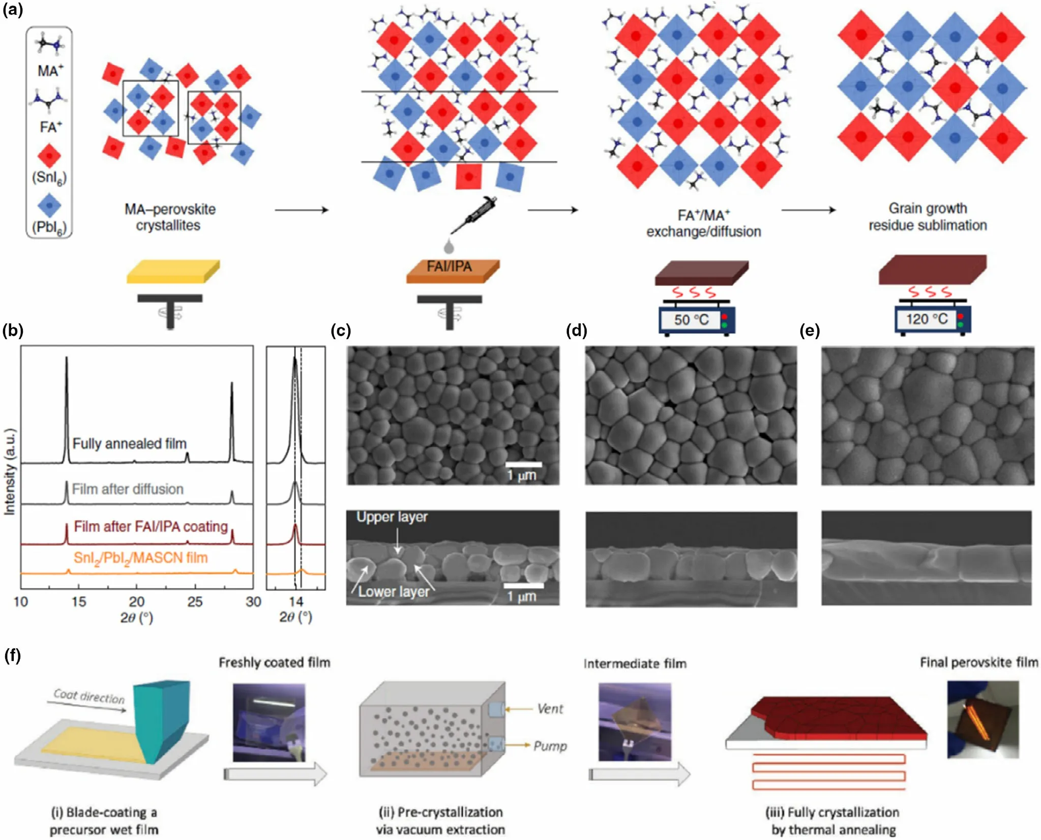
Figure 12. a) Cs0.05MA0.1FA0.83Pb0.5Sn0.5I3 perovskite absorbers prepared by the BIG method b) XRD of the films at each processing stage and SEM images after c) FAI/IPA treatment, d) diffusion stage, and e) final annealing stage (top image: surface view, bottom image: cross section). Reproduced with permission.[41] Copyright © 2020, Springer Nature f) Mixed vacuum and thermal annealing process for blade coated Pb-only and Pb-Sn mixed perovskites.Reproduced with permission.[131] Copyright © 2019, Wiley.
Thermal annealing aids perovskite crystallization from the precursors by removing excess solvent and completing grain growth.[128,129]Thus, the annealing temperature and time as well as other conditions(such as solvent-assisted vapor annealing), morphological control of the perovskite film can be achieved.[63]The temperature must be high enough to fully crystallize the film; however, it should allow all the precursor components to withstand without decomposing,and an optimum annealing duration should be employed to complete the crystallization process.[146]The perovskite composition and thickness decide these parameters, thus should be optimized suitably.[128,129]Generally for Pb-Sn mixed perovskites, an annealing temperature in the range of 70°C to 120°C[1,42,88]and time of 5 min to 30 min[24,37,144]are suitable,the most widely reported being 100°C,10 min.[34,40,130]In some Pb-only PSCs, two-step annealing processes (high-temperature rapid annealing followed by low-temperature brief heating) were explored[147]which improved film morphology resulting in better device performances. This method can also be seen in the more recent studies for Pb-Sn mixed PSCs.[95,142]Another approach is the“solventassisted vapour annealing” where the film is annealed under an environment of saturated solvent(such as DMF)vapor.[148]In this method,the precursor molecules are reorganized with the aid of the solvent vapor that diffuses into the perovskite to result in a high-quality perovskite film. Although this method is commonly seen in sequentially deposited Pb-based perovskites[148]and not yet widely used for Pb-Sn mixed perovskites, a process similar to this method was adapted by Leijtens et al.,for Pb-Sn mixed perovskites using MACl vapor(onestep fabrication of FA0.75Cs0.25Pb0.5Sn0.5I3) to aid grain growth and heal cracks in the films.[13]The researchers followed previous studies in Pb-based PSCs,[149]where the methylamine (CH3NH2) gas-induced defect healing was first reported through the formation of a perovskite-CH3NH2intermediate during the annealing process.Leijtens et al.coupled this method with acidifying the precursor solution using formic acid,to improve the PSC efficiency from 13.1%(of thermally annealed film) to 15.6% with micron-sized grains and increases in device VOCand FF.[13]
Jiang et al. employed a delayed annealing process for MA0.4FA0.6Pb0.4Sn0.6I3perovskites, whereby the fabricated films(toluene anti-solvent) were simply kept in N2glove box for 15 min before annealing at 100°C for 10 min, achieving 18.68% efficiency compared to the 14.47% of reference without the delayed anneal.[150]The improvements were attributed to the slow evaporation of DMSO solvent in the perovskite films with delayed annealing,improving mass transport and diffusion, giving rise to better film quality (more uniform, compact, and pinhole-free layers with reduced surface roughness).[150]
3.3.5. Surface Post-treatments
It was noted in Section 3.3.3 that some additives are used on the perovskite films as a post-treatments. The post-treatments materials are often spin-coated on the perovskite absorber right after its fabrication and annealing in order to facilitate surface passivation (to reduce trap density and thus alleviate non-radiative recombination and extend charge carrier recombination lifetimes),[151]provide protection for the perovskite layer against degradation,[152]dope the perovskite to improve the charge transport[153]and to facilitate larger crystal growth via Ostwald ripening.[154]In Pb-Sn mixed perovskites,the surface treatments are regarded of especial benefit,to hinder the surface Sn2+oxidation by suppressing interaction with adsorbed or atmospheric O2.
In Pb-only perovskites, post-treatments using guanidinium(CH6N3+; GA+) halides are employed for passivation of traps,[153,155,156]to induce Ostwald ripening of grains,[154]to increase the carrier lifetimes,and to increase stability and defect tolerance of the devices by acting as a dopant or alloy.[153,157]Similarly, Sn-only perovskites reported PCE reaching 10% using GA+in FASnI3perovskites doped with 1% EDAI2(ethylenediammonium diiodide) obtaining 9.6%(after storing in an inert environment for 2000 h).[158]The effect of GA+salts in Pb-Sn mixed perovskites has also been reported a few times in very recent studies[7,39]and has proven to be highly effective,thus will be discussed in depth in Section 3.4.3. Other materials based on Lewis-base post-treatments have been reported for Sn-incorporated perovskites, with organic molecules such as ethane-1,2-diamine(edamine) to suppress recombination.[159]More simple methods such as a post solvent wash with a non-polar solvent can be incorporated in the fabrication process to remove the Sn4+dopants on the Pb-Sn mixed perovskites to further suppress the interfacial recombination.[47]Another method yielding high PCEs in Pb-Sn mixed PSCs is the fabrication of a 2D perovskite to act as a protective barrier at the surface,passivating grain boundaries.[130,160]This technique is discussed further in Section 3.4.4.
3.4. Toward Higher Performance of Pb-Sn Mixed PSCs
3.4.1. Suppression of Sn2+Oxidation
As discussed so far,the most prominent issue that limits the maximum performance of Pb-Sn mixed PSCs,the instability of Sn2+.[30,31]Sn4+is the thermodynamically more stable ionic form of Sn, which deems it greatly sensitive to air and moisture, and readily oxidizes as given in Equation 4.

When in the perovskite matrix, this oxidation process produces Sn vacancies which deteriorate the lattice,while the Sn4+ions behave as ptype dopants(holes)in the perovskite.[141,161,162]This hole generation process,known as“self-doping,”can be expressed as per below(Equation 5).[141]

These dopants become trap sites for mobile charge carriers, contributing largely to non-radiative recombination in Sn-containing perovskites.[30,163]Thus, Sn-containing perovskites mostly turn out to be p-type due to the Sn4+doping,and the resulting high concentration of p-type carriers contributes to scattering, in turn reducing the charge carrier mobility.[122]
This persistent phenomenon has caused the Pb-Sn perovskite community to focus widely on defect passivation and inhibiting the oxidation process, which has become key in PCE and stability improvements in these PSCs.[164]The vast majority of Pb-Sn PSCs are processed in controlled environments in the absence of oxygen and moisture, and proper encapsulation is critical for device testing in ambient conditions.[141]Incorporation of ≥50% of Pb2+in Pb-Sn PSCs was reported to significantly decrease the tin oxidation process,[31]as has various additives incorporated in the precursor,the most common being SnF2.[14,31,141]Compared to the typical halides used in metal halide perovskites, F−anion has a much smaller radius (129 pm),[98]too small to inhabit the perovskite crystal lattice, thus segregates at the grain boundaries.[64]Therefore,SnF2does not alter the bandgap, but improves the Pb-Sn perovskite absorber[64,165]when incorporated in small amounts (generally optimized to 20% of overall Sn2+concentration, with further increments SnF2amounts becoming detrimental to the PSC performance).[165]Several adduct forms of SnF2(such as SnF2-DMSO[166]or SnF2-3FACl[118]) were also reported for Pb-Sn PSCs, which aided in trap density reduction resulting in enhanced charge transport through the device.
Other additives in oxidation mitigation include SnF2-pyrazine complexes,[167]ascorbic acid[25](antioxidants), H3PO2acid (reducing agent),[33]and MASCN.[168]Additives such as ascorbic acid have better antioxidant capabilities than SnF2,[25]which could further retard the carrier recombination of Pb-Sn mixed perovskites, improving longterm stability.It was also reported that the perovskite behaves as n-type under the presence of a reducing agent,through successfully suppressing the formation of Sn4+,[33]whereas SCN−from additives such as MASCN form strong interactions with Sn2+preventing its interaction with O2.[168]
Taking these efforts into consideration, a recent study by Mundt et al[169]investigated the origination of Sn2+oxidation and phenomena that govern the process. As the authors point out, the oxidation process occurs not only when the Pb-Sn mixed perovskites are exposed to the atmosphere, but also when the films age inside an inert environment with heavily controlled O2and moisture levels(although film degradation under atmospheric conditions is much more rapid due to higher amounts of O2and moisture). Employing a MA0.4FA0.6Pb0.4Sn0.6I3perovskite absorber,the authors studied the bulk and surface/interface regions of the film upon inert(N2)conditions and under air,at RT and 60°C.[169]In all cases,the results strongly suggest that the bulk crystal structure remains stable under aging,even when subjected to combined external stresses such as heat,electrical bias,and light.Thus,the authors conclude the Sn2+oxidation process affects PSC device performance at the interfaces,introducing surface barriers at the perovskite surface to inhibit efficient charge extraction.The authors further point out the contribution of ionic migration,specifically of I−,which will act as a driving force to the oxidation process, such that it occurs spontaneously even in the absence of other external stresses.Even under inert conditions,the inherent I−in the perovskite as well as small amounts of O2or moisture present inside the glovebox,the precursors and solvents will contribute to Sn2+oxidation and the formation of species such as SnO2, and undercoordinated metal cations (Snδ<2+and Pbδ<2+) on the surface.[169]While the authors suggest this phenomenon can be affected by a variety of different factors including the chemical composition of the perovskite, this study points out the need for proper surface passivation methods in Pb-Sn mixed perovskite absorbers which will be discussed in the next sections of this review.
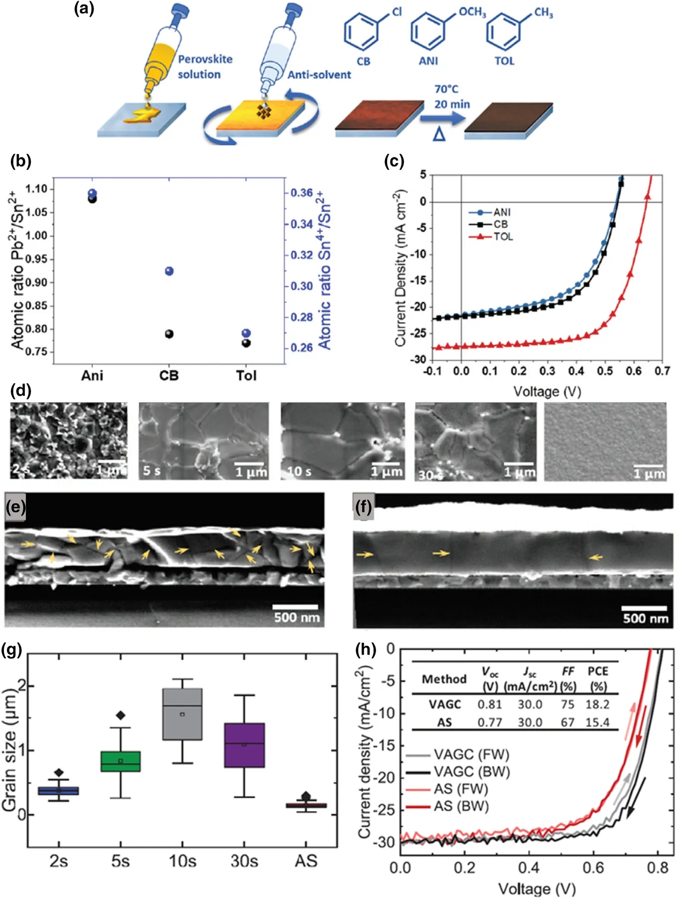
Figure 13. a) Schematic representation of the anti-solvent method with commonly used chlorobenzene(CB), anisole (ANI), and toluene (TOL) molecular structures shown in the inset b) amounts of Sn4+ in the Cs0.05MA0.16FA0.79Pb0.5Sn0.5I3 perovskite absorbers treated by different anti-solvents and c)J-V characteristics of the resulting champion PSC devices showing higher performance for toluene treated device.Reproduced from reference.[47]d)SEM images of MA0.2FA0.8Pb0.5Sn0.5I3 perovskite films grown by vacuum-assisted growth control(VAGC)from left to right;vacuum time 2s,5s,10s,30s,and same perovskite film prepared by antisolvent method. Cross sectional SEM of e) anti-solvent treated and f) VAGC-treated films. g) Grain sizes corresponding to e),and h)J-V characteristics of the champion PSC devices showing higher performance for VAGC device over anti-solvent devices.Reproduced from reference.[144]
3.4.2. Removal and Reduction of Sn4+
As discussed above, there have been a significant amount of effort toward retarding the oxidation of Sn2+; however, much attention has not been given toward tackling the Sn4+amount in the perovskite which may arise from the SnI2precursor itself or during the film formation. On the one hand, non-polar antisolvents such as toluene have been reported to remove some of Sn4+coming from the precursor solution, during the fabrication of the films.[47]On the other hand, some researchers have progressed a step further and succeeded in converting the Sn4+back into Sn2+within the Pb-Sn mixed perovskite solution using metallic Sn powder as a reducing agent (Equation 6),[34,40]inspired by similar work carried out in Sn-only perovskites.[170]

As seen in Figure 14a(left),a regular Pb-Sn mixed perovskite precursor solution takes a yellow color, which, upon exposing to atmospheric conditions, rapidly changes color to take a red hue indicating the oxidation of Sn2+to Sn4+.[34]For a MA0.3FA0.7Pb0.5Sn0.5I3perovskite solution,Lin et al.incorporated a small amount of metallic Sn powder (5 mg ml−1)which not only prevented the oxidation of Sn2+to Sn4+(Figure 14a(right)), but also reduced the Sn4+to Sn2+changing the red solutions back to yellow. This method paves way for the fabrication of Pb-Sn perovskite films in air and improves the device stability.Here, Lin et al. achieved the highest reported PCE at the time of 21.1%(19.5%certified)for Pb-Sn mixed single-junction PSCs.[34]Interestingly, compared to the reference PSC, the incorporation of metallic Sn also affected the trends in performance parameters with film thickness (Figure 14b),giving superior stability in FF irrespective the thickness,and an increase in JSC(as well as the PCE) with increasing thickness (up to 860 nm).In general,better reproducibility of results was achieved with the incorporation of Sn powder,due to the reduction of the Sn vacancies in the perovskite lattice, and increasing the charge carrier diffusion length up to 3 μm.[34]In a similar study by Jiang et al,[40]Sn powder was incorporated in a MA0.4FA0.6Pb0.4Sn0.6I3perovskite formula, to report another remarkable PCE of 20.7%. The authors attributed the high performance to the increased charge carrier lifetimes ~700 ns and higher fill factors of 80.34%due to reduced trap density and recombination.[40]The study also suggested a slight improvement of the surface quality of the Sn4+reduced films.
Despite the high performance reported by Lin et al.,the authors suggested more efforts via device interface and grain passivation in order to achieve higher VOCand FF values.[34]Thus, the same research group attempted a surface-anchoring zwitterionic antioxidant for the same perovskite composition, reporting the next highest PCE of 21.7% (20.7%certified) a year later (Figure 14c-f).[45]This method further inhibited the Sn2+oxidation and passivated the surface and grain boundaries,giving rise to the higher PCE,stability,and uniformity of the devices.Here,a small amount of formamidine sulfinic acid (FSA), a strong reducing agent with a stable zwitterionic configuration,was used in the precursor solution to simultaneously serve multiple functionalities. Although FSA had no effect on the crystallization or film morphology,it significantly suppressed the oxidation on the solid film surface after exposure to air and reduced surface Sn4+to Sn2+by anchoring on the surface and grain boundaries (Figure 14c,d). Furthermore, passivating both electron and hole vacancies in the lattice was achieved due to the zwitterionic nature of FSA, largely reducing the trap density of the MA0.3FA0.7Pb0.5Sn0.5I3absorber,decreasing non-radiative recombination,increasing charge carrier lifetimes,and giving rise to a spatially uniform film(uniform bandgap) which resulted in a higher PCE and better reproducibility(Figure 14e,f).[45]At the time of this review, this report contains the best-certified efficiency value for single-junction Pb-Sn mixed PSC.However,it is worthwhile noting that,to achieve high performance through alleviating Sn4+issue and passivating the surface,SnF2,metallic Sn powder,and FSA zwitterion were all employed in the precursor solution here.This is a clear indication of the efforts that must be taken to tackle the oxidation of Sn2+,and the magnitude of the challenge in reaching the maximum potential of Pb-Sn mixed perovskites. Thus, more efforts toward understanding the retention or removal of Sn4+are still needed in Pb-Sn mixed perovskites.
3.4.3. Surface Passivation with Hetero Structures
As discussed previously, high-quality perovskite films are the key to high-performing PSCs. Generally, for Sn-containing perovskites, the majority of Sn oxidation happens on the surface of the perovskite;thus, a suitable surface passivation technique should be used to protect the perovskite from degradation and improve the film quality.[171]Some theoretical studies on Sn-only CsSnI3perovskite suggest the use of (1) low-dimensional Sn perovskites (such as CsSn2Br5),(2) alkali metal halides, (LiF, LiI, KCl, NaBr, or CsF), or (3) some group 14 oxides (GeO2or SiO2) are the best candidates to protect the Sn perovskite surface.[171]Here, the authors Wei et al. suggest similar materials may benefit Pb-Sn mixed PSCs as well and should be explored further, considering the lattice mismatch and charge transport properties. For Pb-Sn PSCs, low-dimensional perovskites are already used and will be further discussed in Section 3.4.4, and although the metal halide treatments are not widely reported, other salt systems have gained increasing attention in this field. From the recently reported surface treatments, much of the high-performing Pb-Sn perovskites were achieved using guanidinium (GA+) and/or thiocyanate (SCN−) containing salts such as GASCN,[39]GABr,[7,44]KSCN,[142]and Py-SCN.[41]
The first GASCN treatment was employed by Tong et al, in 2019 which proved to give high efficiency of 20.5% from a (FASnI3)0.6(MAPbI3)0.4perovskite absorber, with remarkable charge carrier lifetimes of > 1μs, charge carrier diffusion lengths of ~2.5 μm and an order of magnitude reduction in defect densities. (Figure 15a).[39]Here, GASCN was reported to passivate the grain boundaries which reduced the defect states in surface regions, by forming 2D structures(with yet unknown compositions)which segregate at the grain boundaries. The much wider bandgap of 2D structures passivate the boundaries improving the electronics properties and block Sn diffusion out of the grains and O2diffusion into the grains suppressing the Sn oxidation.[39]In another study employing GA+salts,GABr was used to passivate the Cs0.05FA0.79MA0.16Pb0.5Sn0.5I3triple cation perovskite film by Jayawardena et al.achieving the highest reported fill factor(~83%)for Pb-Sn mixed perovskite absorbers to date with an efficiency of 14.4%(Figure 15b).[7]In Pb-Sn mixed perovskites, fill factors of >80% are seldom reported, and the authors attributed the improvements to surface passivation by salts of large GA+cation aggregated on the surface,as well as the electronic band structure improvements arising from the small Br−ions diffusing through the thickness of the perovskite film,producing a more electron doped perovskite layer.[7]Recently, in another study,12%of GABr was introduced to a FA0.7MA0.3Pb0.7Sn0.3I3by Zhou et al., with an efficiency of 20.63% (19.8% certified).[44]Here, high charge carrier concentrations with reduced trap densities and a reduction of VOCdeficit were reported due to defect passivation by GABr, with improved thermal (90% retention of initial PCE) and environmental stability(85%retention of initial stability)in air without encapsulation (Figure 15c). Generally, all studies on GA+salt treatments reported higher grain sizes and defect passivation. Since Pb-Sn perovskites face arising of a large number of defects due to Sn2+oxidation, GA treatments offer great promise and potential in achieving higher efficiencies and stabilities in these PSCs.
As mentioned above, in the GASCN treatment, formation of a 2D structure was reported.[39]In another study employing SCN−, Li et al.[41]reported a 1.5 mol% incorporation of pyrrolidinium thiocyanate(PySCN)to form a 1D perovskite PySnxPb1-xI3on the surface of Cs0.05FA0.85MA0.1Pb0.5Sn0.5I3to passivate the grain boundaries and the film surface which resulted in 1.1 μm charge carrier lifetimes and 20.4%PCE.[41]The perovskite was fabricated through the two-step BIG process (Section 3.3.1), and PySCN was directly incorporated in the precursor solution resulting in the surface 1D perovskite upon fabrication of the absorber film. With this treatment,the improved HTL/perovskite junction qualities led to enhancements of VOC,FF and the high charge carrier lifetimes reported.[41]In other work, Chen et al. used KSCN in a MA0.5FA0.5Pb0.5Sn0.5I3perovskite[142](Figure 16) resulting in high-quality perovskite films with no pinholes, enhanced crystallinity, and enlarged grain sizes which improved the device PCE owing to a smooth carrier transportation in the film. Here, KSCN was incorporated directly in the precursor film(range of 1–10%),and 7%was found to aid the best performance.In agreement with the previous researchers, the authors suggest that the SCN−ions interact better than I−ions with Pb2+and Sn2+in the perovskite system, which allows them to protect Sn2+from oxidizing as well as allowing slow crystallization of the films.It was also noted that the synergistic effect of both K+and SCN−added together works better in this instance,than adding K+or SCN-alone in the form of other salts, as evident in Figure 16c where 7%KSCN results in a compact film with large grains.During the annealing process, the SCN−was almost completely removed as HSCN gas from the film, whereas the K+ions may have segregated at the grain boundaries passivating the film.[142]
In most high-performing Sn-only perovskites, incorporating EDAI2(ethylenediammonium diiodide) is widely reported to aid passivating the defect states on the surface,reducing pinholes improving film morphology, and alleviating Sn2+oxidation.[46,158,172]Interestingly, many of these devices were found to improve their PCE over time,reaching a maximum after being stored in inert atmosphere for over two months(“slow passivation”).This approach could be further explored in Pb-Sn mixed perovskites as another possible passivation pathway.
3.4.4. Use of Low-Dimensional Perovskites
As mentioned in the previous section, some SCN−passivation layers can give rise to low-dimensional (1D or 2D) perovskites. Similar perovskites, such as 2D Ruddlesden–Popper or 2D Dion–Jacobson structures(Figure 17a and b,respectively),can be used either as functional passivation layers for bulk 3D perovskites or as active layers themselves and is worth exploring further. Interfacial engineering with a 2D perovskite passivation layer first gained significant attention in 2017 when the option of a 2D/3D interface lead to devices that were stable for over 10 000 h.[173]Due to the reduced dimensionality of 2D perovskites,their bandgaps are larger than 3D perovskite counterparts, and the reduced dimensionality and use of large A-site cations make them ideal candidates for passivation, which can decrease unwanted O2or ion migration within devices. Zeng et al. reported a decrease in nonradiative recombination in a 3D Pb-Sn mixed perovskite when a 2D passivation layer was used,increasing PCE from 12.5%to 15%,[174]Li et al. showed that the phenethylammonium (PEA+) A-site can also be used to passivate I−and FA+trap states on the surface of a Pb-Sn perovskite active layer.[175]
Reducing the dimensionality of the perovskite structure from 3D toward a 2D structure presents an opportunity for mixed Pb-Sn materials, as they have been previously shown to regulate the crystallization process, suppress the oxidation of Sn2+to Sn4+, and reduce the environmental impact relative to pure-Pb perovskites.[176–179]The reduced dimensionality of (PEA)2(FA)n−1SnnI3n+1also showed improved thermodynamic stability relative to FASnI3via a reduced decomposition enthalpy with respect to a common oxidation pathway. This was also shown to improve rapidly as n is reduced.This effect,when combined with the hydrophobic nature of the PEA molecule, allows for high device stabilities in Sn-containing 2D and quasi-2D (1 < n < 6) perovskites.[177]Pb-Sn materials also have the distinct advantage of reducing the bandgap relative to pure-Pb perovskites, especially in quasi-2D perovskites of the form A12A2n-1BnX3n+1or A1A2n-1BnX3n+1, where n > 1, as this reduces the bandgap relative to pure 2D phase perovskites, while still maintaining higher stability than 3D perovskites. A bandgap of 1.27 eV has recently been shown for (3AMP)(MA0.5FA0.5)3(Pb0.5Sn0.5)4I13, which was used to improve the device properties of a 3D mixed Pb-Sn perovskite,with improved power conversion efficiency of 20.09% for the mixed Pb-Sn 2D/3D configuration.[43]Much like 3D perovskites,2D mixed Pb-Sn perovskites show a bandgap bowing as a function of increasing Sn content. Due to the reduced dimensionality of 2D perovskites, the band edge dispersion is reduced, resulting in a lower bandgap bowing than 3D perovskites.The bandgap bowing of 2D structures is also less pronounced than that of the 3D structures,with values ranging from 0.352 to 0.918 eV(Figure 17c)relative to 1.08 eV shown for MAPb1-xSnxI3.
4. Outlook and Future Directions
4.1. Review Summary and Highlights
In summary,Pb-Sn mixed perovskites have gained increasing attention especially due to their suitability as narrow-bandgap subcells in allperovskite tandem solar cells. The Pb:Sn metal cation composition in the B site of ABX3perovskite structure directly contributes in tuning the“narrow” bandgap of the absorber generally in the range of 1.2 –1.3 eV, while the X (halide) ion aids in fine-tuning the bandgap further. With the B site, the bandgap shows a “bowing effect” where it decreases with increasing Sn content up to about 50-60% of the B site and then increases when Sn is further increased. In this range, these perovskites can achieve bandgap energies closer to the Shockley–Queisser limit of ~1.3 eV. While reaching this optimum bandgap, various efforts have been taken to increase the efficiencies of these PSCs,achieving 21.7%(20.7%certified)in 2020,the highest reported by the time of this review. However, the maximum performance achievable with these devices has not yet been reached, largely due to the prominent issue of Sn2+oxidation. As such, the efforts taken toward efficiency improvements of Pb-Sn mixed PSCs highlighted in this review can be summarized under three main categories as discussed below:
i)Sn2+oxidation issue and surface passivation:A number of studies tackling the Sn4+issue can be found, the most common being SnF2incorporation into the precursor solution. Additionally, SnF2.3FACl,SnF2-pyrazine complexes, ascorbic acid, H3PO2acid have also been reported. Additives such as these and solvent annealing (e.g., using DMF vapor) also aid in achieving better quality grains and large grain sizes up to micron sizes,in addition to inhibiting Sn2+oxidation.However, very high efficiencies were recently achieved by incorporating a small amount of Sn metallic powder in the precursor,as well as zwitterion incorporation to suppress the Sn4+formation in the Pb-Sn perovskite absorbers. Other factors such as the amount of Pb2+incorporated in the cells (>50% Pb preferred), choice of anti-solvent(toluene preferred), and surface treatments using agents such as SCN−salts can also suppress the Sn4+formation.
According to recent studies, the Sn2+oxidation is more dominant on the perovskite surface and not in the bulk, and the surface Sn4+acts as deep electron traps.[180]Due to this large number of defects inherent in the Sn-containing perovskite films, some form of surface passivation is highly recommended. Organic salts containing SCN−and GA+(such as GASCN, GABr, KSCN, and MASCN) have been recently gaining increasing attention as modes of surface and grain boundary passivation of Pb-Sn mixed perovskites. Various improvements in PSCs leading to efficiency improvements have been reported, including larger grains, grain boundary passivation by formation of 1D or 2D structures, altering the perovskite composition such as Br doping giving rise to better electronic band alignment of the perovskite with interlayers have been reported, along with suppressed Sn2+oxidation due to limited diffusion of O2into the perovskite lattice. Reducing dimensionality of the Pb-Sn mixed perovskites has also proved to mitigate Sn2+oxidation, through promoting higher thermodynamic stability of the resulting perovskite.Other structures such as alkali metal halides, various oxides such as GeO2and SiO2are also potential pathways for future research, as suggested by theoretical studies on Sn-only perovskites, as well as other organic cations such as EDA.
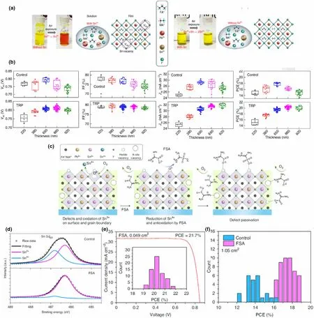
Figure 14. a) Preparation of tin reduced perovskite (TRP) employing small amounts of metallic Sn in the precursor solution, depicting photographs comparing the two precursor solutions (without metallic Sn (left) and with metallic Sn (right)) in ambient air, and illustrations of the formation of Sn vacancies (VSn) in the presence of Sn4+ and suppression of VSn in the absence of Sn4+. b) Corresponding device parameters VOC, FF, JSC, and PCE (from left to right) comparing the control (top) and TRP (bottom) PSC devices with varying thickness of the perovskite film. Reproduced with permission.[34] Copyright© 2019, Springer Nature. c) Schematic illustration of grain boundary defect passivation of Pb-Sn mixed perovskite films by Sn4+ suppression using zwitterion FSA. d) XPS spectra of resulting FA0.7MA0.3Pb0.5Sn0.5I3 perovskite film (bottom) showing flattening of the characteristic Sn4+ peak compared to the control(top), e) J-V characteristics of the champion FSA-treated PSC device measured through 0.049 cm2 aperture (inset shows PCE hysterogram of 65 of said devices, average PCE 20.4 ± 0.5%), and f) PCE hysterogram of 24 control and 47 FSA devices measured under large aperture area 1.05 cm2 (average PCE 13.9 ± 1.0% and 17.5 ± 0.8%, respectively) Reproduced with permission.[45] Copyright © 2020, Springer Nature.
ii)Crystallization and film quality:It is commonly accepted that highquality perovskite films (compact, pinhole-free, highly crystalline with large grain sizes) directly contribute to high-performing PSCs. Pb-Sn mixed perovskites are known to achieve better surface coverage compared to Pb-only analogues owing to the“flower-like”patterns of grain growth.[1,12]The choice of a proper solvent system such as DMSO incorporated DMF has enabled better control over the grain growth,through DMSO-SnI2adduct formation, while employing specific fabrication techniques such as vapor deposition have enabled > 5 μm grain sizes.Br−or Cl−incorporation in Pb-Sn perovskites has also given rise to large grain sizes,high crystallinity,functionalization of grain boundaries,and reduction of electronic disorder,resulting in higher charge carrier lifetimes,carrier mobilities leading to improved PSC performances.
Moreover, different pre- and post-treatments during the fabrication of the perovskite film have been employed such as anti-solvent treatment and various vacuum and solvent annealing techniques. Vacuumassisted crystallization methods allow large and controlled grain growth and generally preferred over anti-solvent treatments that need high precision and purity. However, possibly due to the ease of use, antisolvent method is still seen to be the primary crystallization technique used in Pb-Sn mixed perovskites, generally followed by a thermal annealing step (commonly 100°C, 20 min). Multi-step deposition or multi-step annealing is also seen to produce better results than one-step processes and need to be explored further.
The perovskite composition(including the Pb:Sn ratio)and the film thickness are other factors that strongly affect the grain sizes and morphology.[15]Grain size increments from ~300 to ~1000 nm were reported upon increasing the film thicknesses from 400 nm to 1010 nm,also enabling longer charge carrier lifetimes.[15]Most reports achieving high efficiencies generally report reductions in trap density and recombination in the resulting films.
iii) Selection of interlayers: The importance of suitable interlayers should also be noted here, for a more successful suppression of Sn2+oxidation in the PSCs.PEDOT:PSS is still widely used as HTL for the Pb-Sn mixed perovskites,along with ITO transparent electrode to compose the anode. Previous work has indicated that the quality and morphology of Pb-Sn perovskite films are dependent on the nature of the charge transport layer on which they are fabricated. Favorable effects of an organic/polymer HTL over a metal oxide ETL on the resulting Pb-Sn perovskite film is one of the reasons for the prevailing preference for inverted architectures. Other HTLs such as PTAA and NiOxhave been explored with improvements compared to PEDOT:PSS. Although PEDOT is notorious for its acidity inducing corrosion of ITO electrode,and the fact it can accelerate the Sn2+oxidation with residual moisture,a shift to a different HTL is not yet seen at large in the Pb-Sn mixed PSC community, thus should be further explored. To compose the cathode in these inverted devices,C60/BCP/Ag or PCBM/BCP/Ag are most frequently used as ETL/metal electrode combinations,though other materials such as ZnO or LiF are reported in a limited number of studies.
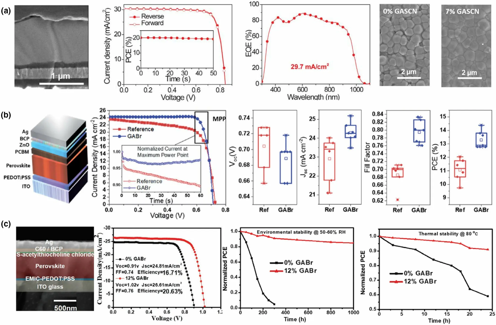
Figure 15. a) PSC characteristics containing (FASnI3)0.6(MAPbI3)0.4 perovskite absorber modified with 7% GASCN. From left to right; cross section SEM image of perovskite film modified with 7% GASCN, J-V curve of the champion single-junction Pb-Sn mixed PSC with the GASCN treated perovskite layer (with stabilized power output tracking at maximum power point given in the inset), the EQE spectrum for the champion device, top SEM images of the perovskite films without and with 7% GASCN surface treatment. Reproduced with permission.[39] Copyright © 2019, American Association for the Advancement of Science. b) PSC characteristics containing Cs0.05FA0.79MA0.16Pb0.5Sn0.5I3 perovskite absorber modified with GABr surface treatment. From Left to right;schematic image of PSC device, J-V curve of the champion single-junction reference device and device with the GABr-treated perovskite layer (with stabilized power output tracking at maximum power point given in the inset), VOC, JSC, FF and PCE of the said reference and GABr-treated devices. Reproduced with permission.[7] Copyright © 2019, Royal Society of Chemistry. c) PSC characteristics containing FA0.7MA0.3Pb0.7Sn0.3I3 perovskite absorber modified with GABr surface treatment. From Left to right; cross section SEM image of PSC device, J-V curve of the champion single-junction devices with 0% and 12% GABr incorporated perovskite absorber, environmental stability of the said devices with 50%-60% relative humidity in air, thermal stability of the devices upon heating for 24 h at 80°C in air. Reproduced with permission.[44] Copyright © 2020, Wiley.
4.2. Current Applications: Tandem Solar Cells
As discussed earlier, the performance of single-junction PSCs is limited by the Shockley–Queisser limit, which usually falls at around 33%[109]and tandem cell structures are being explored as a solution. All-perovskite tandem cell structures can be fabricated using printing technologies that can result in high-performing devices with low-cost manufacturability. The bandgap of Pbbased PSCs usually falls in the range of 1.48 – 2.3 eV,[3]which makes them excellent candidates for the wide-bandgap/top cell with Pb-Sn mixed PSCs ( 1.2 – 1.3 eV)[181]for the narrowbandgap/bottom cell of an all-perovskite tandem structure. Tandem cell structures usually consist of two or more PSCs connected together in either a 2-terminal (2T) configuration or a 4-terminal(4T) configuration.[6]In a 2T or monolithic tandem configuration,the top and bottom devices are fabricated with interconnecting layers(ICLs)between them whereas in a 4T configuration the top and bottom cells are mechanically stacked on top of each other and connected in series using electrodes. The main benefit of 2T tandem solar cells is their simplicity and the low cost of fabrication due to the possibility of using low-temperature processing techniques such as solution processing. However, in this case, the challenge is in precise current matching between the top and bottom cells to optimize the cell performance as well as fabricating ICLs that can act as a barrier which prevents the dissolution of the bottom cell when depositing the respective top cell, along with minimal optical and voltage losses.[6]Even though the 4T tandem architecture does not require strict bandgap matching between top and bottom cells, it requires two extra electrodes to build a connection between the two cells which increases the manufacturing cost of tandem cells with such architectures.
The potential of an all-perovskite tandem cell was first published in late 2014 via optical modeling where the researchers presented a simple monolithic configuration where the top and the bottom layers of the tandem were separated by the HTL and the ETL between them.[182]Before incorporating Pb-Sn mixed perovskites, the first experimentally reported all-perovskite tandem solar cell comprised of a 4T structure consisting of a MAPbBr3(Eg= 2.3 eV) top cell and MAPbI3(Eg=1.55 eV) bottom cell. The device was reported to achieve a VOCof 2.24 V in series connection and a PCE of 8.30%.[183]Heo et al. in 2015 demonstrated a tandem cell with a 2T configuration which was fabricated by sandwiching the two substrates containing the top MAPbBr3(Eg= 2.25 eV) cell and bottom MAPbI3(Eg= 1.55 eV) cell together by pressuring with a double clip and subsequent drying.This technique yielded the first publication of a monolithic tandem solar cell which had a PCE of 10.8%and a VOCof 1.95 V.[184]
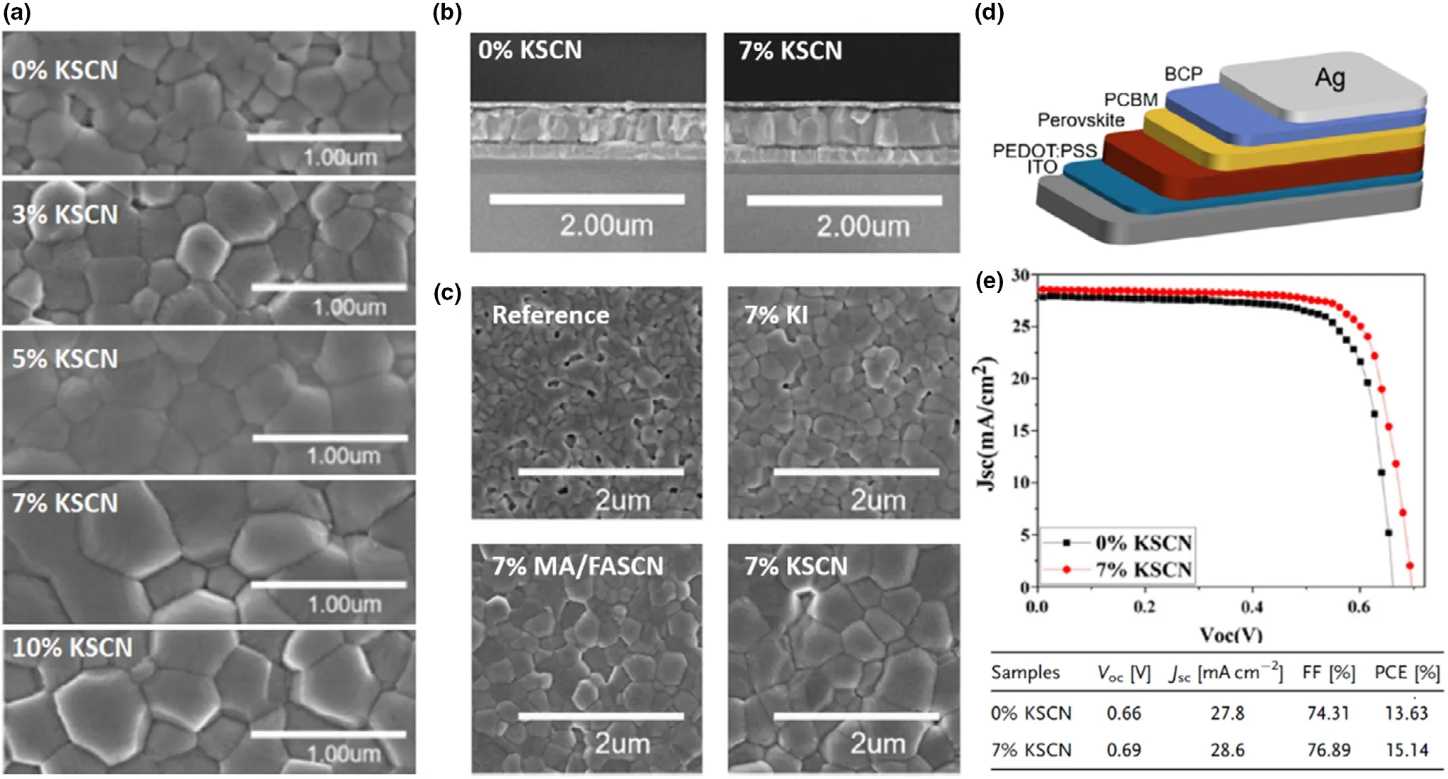
Figure 16. SEM images of a) surface of MA0.5FA0.5Pb0.5Sn0.5I3 perovskite films doped with different concentrations of KSCN, b) cross section SEM of the reference and 7% KSCN-treated perovskite film, and c) surface of reference perovskite and surface treated with 7% KI, 7% MA/FASCN and 7% KSCN, where KSCN treatment shows the largest grains. d) Corresponding device architecture and e) J-V characteristics of the champion reference and 7% KSCN-treated perovskites. Reproduced with permission.[142] Copyright © 2020, Wiley.

Figure 17. Illustration of a) a 2D Ruddlesden–Popper perovskite of the form A2BX4, b) a 2D Dion–Jacobson perovskite of the form ABX4 and c) a description of the various bandgap bowing in mixed solid solution 2D perovskites where BZA = benzylammonium, HA = histammonium, S-MBA = the s orientation of chiral methylbenzylammonium and PEA = phenethylammonium, the x-axis shows Sn content and the y axis shows the bandgap of the structure measured from optical absorption spectroscopy or calculated using DFT.[192-196]
Use of Pb-Sn mixed perovskites in a tandem structure was first published by Yang et al. where wide-bandgap perovskite with a MAPbI3absorption layer was used as the top cell and a narrow-bandgap perovskite with a MA0.5FA0.5Pb0.75Sn0.25I3(Eg=Eg=1.38 eV)was used to fabricate a 4T tandem solar cell that achieved a combined PCE of 19.08%.[11]On 2T architectures, the first reported perovskite/perovskite tandem cell was made using a 1.2 eV bandgap bottom cell with perovskite composition FA0.75Cs0.25Sn0.5Pb0.5I3and a top cell with a bandgap of 1.8 eV and composition FA0.83Cs0.17Pb(I0.5Br0.5)3.[1]The monolithic cell was able to achieve an efficiency of 16.9%and a VOCof 1.66 V. As of present, the highest reported monolithic all-perovskite solar cell has achieved a PCE of 24.8%and a VOCof 1.96 V while retaining 90% of its initial performance after operating for 436 h under 1-sun illumination at maximum power point.[34]This shows promising stability for the Pb-Sn mixed perovskite, which was fabricated using metallic Sn powder to implement stability as discussed in Section 3.4.2.The tandem device consisted of a top cell with an absorption layer Cs0.2FA0.8PbI1.8Br1.2(Eg=1.77 eV) and a bottom cell with an absorption layer FA0.7MA0.3Pb0.5Sn0.5I3(Eg= 1.22 eV).[34]With further optimization of Pb-Sn mixed PSC bottom cells along with the ICLs, all-perovskite tandem solar cells show a promising future to overcome the performance limitations of singlejunction devices through simple fabrication techniques.
4.3. Future Directions
In improving Pb-Sn PSCs, it should be noted here that the major efficiency improvements are still seen when the surface passivation or Sn4+suppression techniques were employed.The ultimate goal in the development of Pb-Sn PSCs,as with any PV device,is their largescale manufacturing. When fabricating tandem solar cells,unlike Pb-only wide-bandgap PSCs,the ambient air manufacturing of Pb-Sn perovskites is still a challenge due to the ambient instability discussed.With increasing Sn content, the crystallization of the perovskite becomes faster[185]and is more difficult to control in a roll-to-roll process. With various strides made in increasing the device stability and efficiency, Pb-Sn PSC research must now explore more large area fabrication techniques, and ambient fabrication techniques, to point the field toward real-world applications. Only a limited number of reports are currently available for Pb-Sn PSCs large area fabrication, such as the study by Li et al,which discusses Pb-Sn mixed PSCs with 1 cm2active area using doctor blading technique.[130]Along with the techniques to suppress Sn2+oxidation, proper encapsulation methods need to be secured to achieve longterm stability of the cells against moisture and oxygen.[186]Another challenge in high-throughput manufacturing of Pb-Sn PSCs is the toxicity of the solvents used such as DMF and DMSO.[6]Compared to the Pb-only perovskites, alternative green solvents have not been widely studied for Pb-Sn mixed PSCs and should be investigated further. More importantly, with the recent findings in Sn-only perovskites where DMSO was found to contribute to Sn2+oxidation,[137]testing alternate solvent systems is an important path for research in Pb-Sn perovskites.Thus,as future directions,the passivation of grain boundaries and reducing surface and bulk trap densities are key points in enhancing the performance of Pb-Sn mixed perovskite films.As discussed so far,much of the field of Pb-Sn mixed perovskites is still to be explored, and there is a large number of interdependent factors affecting the device performance. Thus, a collective effort from the researchers to understand and improve the most crucial parameters is critical in reaching the maximum benefit of these devices.
Acknowledgements
R.M.I.B.and S.M.S.gratefully acknowledge support from the University of Surrey scholarships. R. M. I. B., R. A. S., C. C. L. U., and S. R. P. S. also acknowledge funding from EPSRC (EP/R028559/1 and GR/1922310/1). S. M. S. and S. R. P. S acknowledge support SilverRay Ltd.K.D.G.I.J.and S.R.P.S.gratefully acknowledge financial support from the Equality Foundation of Hong Kong
Conflict of Interest
The authors declare no conflict of interest.
Keywords
inorganic–organic hybrids, lead–tin mixed perovskites, perovskites,photovoltaics, solution-processed
Received: February 14, 2021
Revised: April 8, 2021
Published online: May 7, 2021
[1] G. E. Eperon, T. Leijtens, K. A. Bush, R. Prasanna, T. Green, J.- T.-W.Wang, D. P. McMeekin, G. Volonakis, R. L. Milot, R. May, A. Palmstrom, D. J. Slotcavage, R. A. Belisle, J. B. Patel, E. S. Parrott, R. J. Sutton, W. Ma, F. Moghadam, B. Conings, A. Babayigit, H.-G. Boyen, S.Bent, F. Giustino, L. M. Herz, M. B. Johnston, M. D. McGehee, H. J.Snaith, Science 2016, 354, 861.
[2] B.Zhao,M.Abdi-Jalebi,M.Tabachnyk,H.Glass,V.S.Kamboj,W.Nie,A.J.Pearson,Y.Puttisong,K.C.G¨odel,H.E.Beere,D.A.Ritchie,A.D.Mohite,S.E.Dutton,R.H.Friend,A.Sadhanala,Adv.Mater.2017,29,1604744.
[3] R. Prasanna, A. Gold-Parker, T. Leijtens, B. Conings, A. Babayigit, H.-G.Boyen, M. F. Toney, M. D. McGehee, J. Am. Chem. Soc. 2017, 139,11117.
[4] D. P. McMeekin, S. Mahesh, N. K. Noel, M. T. Klug, J. C. Lim, J. H.Warby, J. M. Ball, L. M. Herz, M. B. Johnston, H. J. Snaith, Joule 2019,3, 387.
[5] A. F. Palmstrom, G. E. Eperon, T. Leijtens, R. Prasanna, S. N. Habisreutinger, W. Nemeth, E. A. Gaulding, S. P. Dunfield, M. Reese, S.Nanayakkara, T. Moot, J. Werner, J. Liu, B. To, S. T. Christensen, M. D.McGehee, M. F. A. M. van Hest, J. M. Luther, J. J. Berry, D. T. Moore,Joule 2019, 3, 2193.
[6] K. D. G. I. Jayawardena, S. M. Silva, R. K. Misra, J. Mater. Chem. C 2020, 8, 10641.
[7] K. D. G. I. Jayawardena, R. M. I. Bandara, M. Monti, E. Butler-Caddle, T.Pichler, H. Shiozawa, Z. Wang, S. Jenatsch, S. J. Hinder, M. G. Masteghin, M. Patel, H. M. Thirimanne, W. Zhang, R. A. Sporea, J. Lloyd-Hughes, S. R. P. Silva, J. Mater. Chem. A 2020, 8, 693.
[8] D. Chi, S. Huang, M. Zhang, S. Mu, Y. Zhao, Y. Chen, J. You, Adv.Funct. Mater. 2018, 28, 1804603.
[9] Z. Yang, A. Rajagopal, A. K. Y. Jen, Adv. Mater. 2017, 29, 1704418.
[10] F. Hao, C. C. Stoumpos, R. P. H. Chang, M. G. Kanatzidis, J. Am. Chem.Soc. 2014, 136, 8094.
[11] Z. Yang, A. Rajagopal, C.-C. Chueh, S. B. Jo, B. Liu, T. Zhao, A.- K.-Y.Jen, Adv. Mater. 2016, 28, 8990.
[12] F. Zuo, S. T. Williams, P.-W. Liang, C.-C. Chueh, C.-Y. Liao, A.- K.-Y.Jen, Adv. Mater. 2014, 26, 6454.
[13] T. Leijtens, R. Prasanna, K. A. Bush, G. Eperon, J. A. Raiford, A. Gold-Parker, E. J. Wolf, S. A. Swifter, C. C. Boyd, H.-P. Wang, M. F. Toney, S.Bent, M. D. McGehee, Sustain. Energy Fuels 2018, 2, 2450.
[14] W. Liao, D. Zhao, Y. Yu, N. Shrestha, K. Ghimire, C. R. Grice, C. Wang,Y. Xiao, A. J. Cimaroli, R. J. Ellingson, N. J. Podraza, K. Zhu, R.-G. Xiong,Y. Yan, J. Am. Chem. Soc. 2016, 138, 12360.
[15] D. Zhao, Y. Yu, C. Wang, W. Liao, N. Shrestha, C. R. Grice, A. J. Cimaroli, L. Guan, R. J. Ellingson, K. Zhu, X. Zhao, R.-G. Xiong, Y. Yan, Nat.Energy 2017, 2, 17018.
[16] L. Zhu, B. Yuh, S. Schoen, X. Li, M. Aldighaithir, B. J. Richardson, A.Alamer, Q. Yu, Nanoscale 2016, 8, 7621.
[17] M. Lyu, M. Zhang, N. A. Cooling, Y. Jiao, Q. Wang, J.-H. Yun, B.Vaughan, G. Triani, P. Evans, X. Zhou, K. Feron, A. Du, P. Dastoor, L.Wang, Sci. Bull. 2016, 61, 1558.
[18] Y. Li, W. Sun, W. Yan, S. Ye, H. Rao, H. Peng, Z. Zhao, Z. Bian, Z. Liu,H. Zhou, C. Huang, Adv. Energy Mater. 2016, 6, 1601353.
[19] G. Lin, Y. Lin, H. Huang, R. Cui, X. Guo, B. Liu, J. Dong, X. Guo, B. Sun,Nano Energy 2016, 27, 638.
[20] L. Li, F. Zhang, Y. Hao, Q. Sun, Z. Li, H. Wang, Y. Cui, F. Zhu, J. Mater.Chem. C 2017, 5, 2360.
[21] H. L. Zhu, J. Xiao, J. Mao, H. Zhang, Y. Zhao, W. C. H. Choy, Adv.Funct. Mater. 2017, 27, 1605469.
[22] J. Liang, P. Zhao, C. Wang, Y. Wang, Y. Hu, G. Zhu, L. Ma, J. Liu, Z. Jin,J. Am. Chem. Soc. 2017, 139, 14009.
[23] Y. Ogomi, A. Morita, S. Tsukamoto, T. Saitho, N. Fujikawa, Q. Shen, T.Toyoda, K. Yoshino, S. S. Pandey, T. Ma, S. Hayase, J. Phys. Chem. Lett.2014, 5, 1004.
[24] G. Kapil, T. S. Ripolles, K. Hamada, Y. Ogomi, T. Bessho, T. Kinoshita, J.Chantana, K. Yoshino, Q. Shen, T. Toyoda, T. Minemoto, T. N. Murakami, H. Segawa, S. Hayase, Nano Lett. 2018, 18, 3600.
[25] X. Xu, C.-C. Chueh, Z. Yang, A. Rajagopal, J. Xu, S. B. Jo, A.- K.-Y. Jen,Nano Energy 2017, 34, 392.
[26] X. Liu, Z. Yang, C.-C. Chueh, A. Rajagopal, S. T. Williams, Y. Sun, A.-K.-Y. Jen, J. Mater. Chem. A 2016, 4, 17939.
[27] Z. Yang, A. Rajagopal, S. B. Jo, C.-C. Chueh, S. Williams, C.-C. Huang, J.K. Katahara, H. W. Hillhouse, A.- K.-Y. Jen, Nano Lett. 2016, 16, 7739.
[28] A. Rajagopal, Z. Yang, S. B. Jo, I. L. Braly, P.-W. Liang, H. W. Hillhouse,A.- K.-Y. Jen, Adv. Mater. 2017, 29, 1702140.
[29] C. Liu, J. Fan, H. Li, C. Zhang, Y. Mai, Sci. Rep. 2016, 6, 35705.
[30] J. Fan, C. Liu, H. Li, C. Zhang, W. Li, Y. Mai, Chemsuschem 2017, 10,3839.
[31] T. Leijtens, R. Prasanna, A. Gold-Parker, M. F. Toney, M. D. McGehee,ACS Energy Lett. 2017, 2, 2159.
[32] R. E. Beal, D. J. Slotcavage, T. Leijtens, A. R. Bowring, R. A. Belisle, W.H. Nguyen, G. F. Burkhard, E. T. Hoke, M. D. McGehee, J. Phys. Chem.Lett. 2016, 7, 746.
[33] C. C. Stoumpos, C. D. Malliakas, M. G. Kanatzidis, Inorg. Chem. 2013,52, 9019.
[34] R. Lin, K. Xiao, Z. Qin, Q. Han, C. Zhang, M. Wei, M. I. Saidaminov, Y.Gao, J. Xu, M. Xiao, A. Li, J. Zhu, E. H. Sargent, H. Tan, Nat. Energy 2019, 4, 864.
[35] M. Anaya, J. P. Correa-Baena, G. Lozano, M. Saliba, P. Anguita, B.Roose, A. Abate, U. Steiner, M. Gr¨atzel, M. E. Calvo, A. Hagfeldt, H.M´ıguez, J. Mater. Chem. A 2016, 4, 11214.
[36] C. Liu, W. Li, H. Li, C. Zhang, J. Fan, Y. Mai, Nanoscale 2017, 9, 13967.
[37] L. Ji, X. Zhang, T. Zhang, Y. Wang, F. Wang, Z. Zhong, Z. D. Chen, Z.Xiao, L. Chen, S. Li, J. Mater. Chem. A 2019, 7, 9154.
[38] Z. Zhu, N. Li, D. Zhao, L. Wang, A.- K.-Y. Jen, Adv. Energy Mater. 2019,9, 1802774.
[39] J. Tong, Z. Song, D. H. Kim, X. Chen, C. Chen, A. F. Palmstrom, P. F.Ndione, M. O. Reese, S. P. Dunfield, O. G. Reid, J. Liu, F. Zhang, S. P.Harvey, Z. Li, S. T. Christensen, G. Teeter, D. Zhao, M. M. Al-Jassim, M.F. A. M. van Hest, M. C. Beard, S. E. Shaheen, J. J. Berry, Y. Yan, K.Zhu, Science 2019, 364, 475.
[40] T. Jiang, Z. Chen, X. Chen, T. Liu, X. Chen, W. E. I. Sha, H. Zhu, Y.Yang, Sol. RRL 2020, 4, 1900467.
[41] C. Li, Z. Song, C. Chen, C. Xiao, B. Subedi, S. P. Harvey, N. Shrestha, K.K. Subedi, L. Chen, D. Liu, Y. Li, Y. W. Kim, C. Sheng Jiang, M. J.Heben, D. Zhao, R. J. Ellingson, N. J. Podraza, M. Al-Jassim, Y. Yan Nat.Energy 2020, 5, 768.
[42] J. Werner, T. Moot, T. A. Gossett, I. E. Gould, A. F. Palmstrom, E. J.Wolf, C. C. Boyd, M. F. A. M. Van Hest, J. M. Luther, J. J. Berry, M. D.McGehee, ACS Energy Lett. 2020, 5, 1215.
[43] W. Ke, C. Chen, I. Spanopoulos, L. Mao, I. Hadar, X. Li, J. M. Hoffman,Z. Song, Y. Yan, M. G. Kanatzidis, J. Am. Chem. Soc. 2020, 142, 15049.
[44] X. Zhou, L. Zhang, X. Wang, C. Liu, S. Chen, M. Zhang, X. Li, W. Yi, B.Xu, Adv. Mater. 2020, 32, 1908107.
[45] K. Xiao, R. Lin, Q. Han, Y. Hou, Z. Qin, H. T. Nguyen, J. Wen, M. Wei,V. Yeddu, M. I. Saidaminov, Y. Gao, X. Luo, Y. Wang, H. Gao, C.Zhang, J. Xu, J. Zhu, E. H. Sargent, H. Tan, Nat. Energy 2020, 5, 870.
[46] K.Nishimura,M.A.Kamarudin,D.Hirotani,K.Hamada,Q.Shen,S.Iikubo,T.Minemoto,K.Yoshino,S.Hayase,Nano Energy 2020,74,104858.
[47] R. M. I. Bandara, K. D. G. I. Jayawardena, S. O. Adeyemo, S. J. Hinder, J.A. Smith, H. M. Thirimanne, N. C. Wong, F. M. Amin, B. G. Freestone,A. J. Parnell, D. G. Lidzey, H. J. Joyce, R. A. Sporea, S. R. P. Silva, J.Mater. Chem. C 2019, 7, 8389.
[48] N.-G. Park, Mater. Today 2015, 18, 65.
[49] Y. Yamada, T. Nakamura, M. Endo, A. Wakamiya, Y. Kanemitsu, J. Am.Chem. Soc. 2014, 136, 11610.
[50] N.Marinova,S.Valero,J.L.Delgado,J.Colloid Interface Sci.2017,488,373.
[51] A. J. Heeger, Adv. Mater. 2014, 26, 10.
[52] G. Yu, J. Gao, J. C. Hummelen, F. Wudl, A. J. Heeger, Science 1995, 270,1789.
[53] V. D’Innocenzo, G. Grancini, M. J. P. Alcocer, A. R. S. Kandada, S. D.Stranks, M. M. Lee, G. Lanzani, H. J. Snaith, A. Petrozza, Nat. Commun.2014, 5, 3586.
[54] K. Galkowski, A. Mitioglu, A. Miyata, P. Plochocka, O. Portugall, G. E.Eperon, J.- T.-W. Wang, T. Stergiopoulos, S. D. Stranks, H. J. Snaith, R.J. Nicholas, Energy Environ. Sci. 2016, 9, 962.
[55] C. Wehrenfennig, M. Liu, H. J. Snaith, M. B. Johnston, L. M. Herz, J.Phys. Chem. Lett. 2014, 5, 1300.
[56] K. Galkowski, A. Surrente, M. Baranowski, B. Zhao, Z. Yang, A. Sadhanala, S. Mackowski, S. D. Stranks, P. Plochocka 2019, 8, 35.
[57] D. E. Carlson, C. R. Wronski, Appl. Phys. Lett. 1976, 28, 671.
[58] E. A. Schiff, S. Hegedus, X. Deng, , in Handb. Photovolt. Sci. Eng., John Wiley & Sons, Ltd, Chichester, UK, 2011, pp. 487–545.
[59] C. Wang, Z. Song, C. Li, D. Zhao, Y. Yan, Adv. Funct. Mater. 2019,1808801.
[60] L. M. Herz, ACS Energy Lett. 2017, 2, 1539.
[61] K. Miyano, N. Tripathi, M. Yanagida, Y. Shirai, Acc. Chem. Res. 2016,49, 303.
[62] C. S. Ponseca, T. J. Savenije, M. Abdellah, K. Zheng, A. Yartsev, T.Pascher, T. Harlang, P. Chabera, T. Pullerits, A. Stepanov, J.-P. Wolf, V.Sundstr¨om, J. Am. Chem. Soc. 2014, 136, 5189.
[63] A. K. Jena, A. Kulkarni, T. Miyasaka, Chem. Rev. 2019, 119, 3036.
[64] M. Konstantakou, T. Stergiopoulos, J. Mater. Chem. A 2017, 5, 11518.
[65] W. Liao, D. Zhao, Y. Yu, C. R. Grice, C. Wang, A. J. Cimaroli, P. Schulz,W. Meng, K. Zhu, R.-G. Xiong, Y. Yan, Adv. Mater. 2016, 28, 9333.
[66] J. Werner, G. Dubuis, A. Walter, P. L¨oper, S.-J. Moon, S. Nicolay, M.Morales-Masis, S. De Wolf, B. Niesen, C. Ballif, Sol. Energy Mater. Sol.Cells 2015, 141, 407.
[67] P. You, Z. Liu, Q. Tai, S. Liu, F. Yan, Adv. Mater. 2015, 27, 3632.
[68] Y. Zong, N. Wang, L. Zhang, M.-G. Ju, X. C. Zeng, X. W. Sun, Y. Zhou,N. P. Padture, Angew. Chemie Int. Ed. 2017, 56, 12658.
[69] A. Klein, C. K¨orber, A. Wachau, F. S¨auberlich, Y. Gassenbauer, S. P.Harvey, D. E. Proffit, T. O. Mason, Materials (Basel). 2010, 3, 4892.
[70] Y. Meng, Z. Hu, N. Ai, Z. Jiang, J. Wang, J. Peng, Y. Cao, A. C. S. Appl,Mater. Interfaces 2014, 6, 5122.
[71] G. Kapil, T. Bessho, C. H. Ng, K. Hamada, M. Pandey, M. A. Kamarudin,D. Hirotani, T. Kinoshita, T. Minemoto, Q. Shen, T. Toyoda, T. N. Murakami, H. Segawa, S. Hayase, ACS Energy Lett. 1991, 2019, 4.
[72] I. Hussain, H. Phong Tran, J. Jaksik, J. Moore, N. Islam, M. Jasim Uddin,Emergent Mater. 2018, 1, 133.
[73] W. Ke, G. Fang, Q. Liu, L. Xiong, P. Qin, H. Tao, J. Wang, H. Lei, B. Li, J.Wan, G. Yang, Y. Yan, J. Am. Chem. Soc. 2015, 137, 6730.
[74] T. Qin, W. Huang, J. E. Kim, D. Vak, C. Forsyth, C. R. McNeill, Y. B.Cheng, Nano Energy 2017, 31, 210.
[75] X.Wang,L.L.Deng,L.Y.Wang,S.M.Dai,Z.Xing,X.X.Zhan,X.Z.Lu,S.Y.Xie,R.Bin Huang,L.S.Zheng,J.Mater.Chem.A 2017,5,1706.
[76] P. Zhang, J. Wu, T. Zhang, Y. Wang, D. Liu, H. Chen, L. Ji, C. Liu, W.Ahmad, Z. D. Chen, S. Li, Adv. Mater. 2018, 30, 1703737.
[77] K.-H. Jung, J.-Y. Seo, S. Lee, H. Shin, N.-G. Park, J. Mater. Chem. A 2017,5, 24790.
[78] Y. Wang, W. Fu, J. Yan, J. Chen, W. Yang, H. Chen, J. Mater. Chem. A 2018, 6, 13090.
[79] S. Gubbala, V. Chakrapani, V. Kumar, M. K. Sunkara, Adv. Funct.Mater. 2008, 18, 2411.
[80] D. Yang, R. Yang, K. Wang, C. Wu, X. Zhu, J. Feng, X. Ren, G. Fang, S.Priya, S. Liu, Nat. Commun. 2018, 9, 3239.
[81] S. Shao, Y. Cui,H.Duim,X. Qiu, J. Dong, G.H.ten Brink,G. Portale, R. C.Chiechi,S.Zhang,J.Hou,M.A.Loi,Adv.Mater.2018,30,1803703.
[82] M. Liu, Z. Chen, Q. Xue, S. H. Cheung, S. K. So, H.-L. Yip, Y. Cao, J.Mater. Chem. A 2018, 6, 16347.
[83] A. N. Cho, N. G. Park, Chemsuschem 2017, 10, 3687.
[84] N. Shibayama, H. Kanda, T. W. Kim, H. Segawa, S. Ito, APL Mater.2019, 7, 31117.
[85] G. Niu, X. Guo, L. Wang, J. Mater. Chem. A 2015, 3, 8970.
[86] J. Burschka, F. Kessler, M. K. Nazeeruddin, M. Gr¨atzel, Chem. Mater.2013, 25, 2986.
[87] J. Carrillo, A. Guerrero, S. Rahimnejad, O. Almora, I. Zarazua, E. Mas-Marza, J. Bisquert, G. Garcia-Belmonte, Adv. Energy Mater. 2016, 6,1502246.
[88] Y. Yao, F. Lv, L. Luo, L. Liao, G. Wang, D. Liu, C. Xu, G. Zhou, X. Zhao,Q. Song, Sol. RRL 2020, 4, 1.
[89] M. P. De Jong, L. J. Van Ijzendoorn, M. J. A. De Voigt, Appl. Phys. Lett.2000, 77, 2255.
[90] M. Zhang, D. Chi, J. Wang, F. Wu, S. Huang, Sol. Energy 2020, 201, 589.
[91] C. Y. Chang, B. C. Tsai, Y. C. Hsiao, M. Z. Lin, H. F. Meng, Nano Energy 2019, 55, 354.
[92] M. B. Islam, M. Yanagida, Y. Shirai, Y. Nabetani, K. Miyano, ACS Omega 2017, 2, 2291.
[93] J. A. Christians, R. C. M. Fung, P. V. Kamat, J. Am. Chem. Soc. 2014,136, 758.
[94] N. Arora, M. I. Dar, A. Hinderhofer, N. Pellet, F. Schreiber, S. M.Zakeeruddin, M. Gr¨atzel, Science 2017, 358, 768.
[95] H. Chen, Z. Peng, K. Xu, Q. Wei, D. Yu, C. Han, H. Li, Z. Ning, Sci.China Mater. 2020, 64, 537.
[96] B. Jaffe, W. R. Cook, H. L. Jaffe, Piezoelectric Ceramics, Academic Press 1971.
[97] S. Wan-Jian Yin, S.-H. Wei, W.-J. Yin, A. Ji-Hui Yang, J. Kang, Y. Yan, J.Mater. Chem. A 2015, 3, 8926.
[98] S. F. Hoefler, G. Trimmel, T. Rath, Monatshefte f¨ur Chemie - Chem.Mon. 2017, 148, 795.
[99] T.Umebayashi,K.Asai,T.Kondo,A.Nakao,Phys.Rev.B 2003,67,155405.
[100] B. Wang, X. Xiao, T. Chen, Nanoscale 2014, 6, 12287.
[101] Q. Chen, N. De Marco, Y. Yang, T. Bin Song, C. C. Chen, H. Zhao, Z.Hong, H. Zhou, Y. Yang, Nano Today 2015, 10, 355.
[102] T. Leijtens, K. Bush, R. Cheacharoen, R. Beal, A. Bowring, M. D. McGehee, J. Mater. Chem. A 2017, 5, 11483.
[103] E.Smecca,Y.Numata,I.Deretzis,G.Pellegrino,S.Boninelli,T.Miyasaka,A.La Magna,A.Alberti,Phys.Chem.Chem.Phys.2016,18,13413.
[104] G. Niu, W. Li, J. Li, X. Liang, L. Wang, RSC Adv. 2017, 7, 17473.
[105] Z. Li, M. Yang, J. S. Park, S. H. Wei, J. J. Berry, K. Zhu, Chem. Mater.2016, 28, 284.
[106] M. Saliba, T. Matsui, J.-Y. Seo, K. Domanski, J.-P. Correa-Baena, M. K.Nazeeruddin, S. M. Zakeeruddin, W. Tress, A. Abate, A. Hagfeldt, M.Gr¨atzel, Energy Environ. Sci. 1989, 2016, 9.
[107] T. Singh, T. Miyasaka, Adv. Energy Mater. 2018, 8, 1700677.
[108] T. J. Jacobsson, S. Svanstr¨om, V. Andrei, J. P. H. Rivett, N. Kornienko, B.Philippe, U. B. Cappel, H. Rensmo, F. Deschler, G. Boschloo, J. Phys.Chem. C 2018, 122, 13548.
[109] W. Shockley, H. J. Queisser, J. Appl. Phys. 1961, 32, 510.
[110] J. Liu, G. Wang, Z. Song, X. He, K. Luo, Q. Ye, C. Liao, J. Mei, J. Mater.Chem. A 2017, 5, 9097.
[111] F. Cao, J. Chen, D. Yu, S. Wang, X. Xu, J. Liu, Z. Han, B. Huang, Y. Gu,K. L. Choy, H. Zeng, Adv. Mater. 2020, 32, 1905362.
[112] F. Valadares, I. Guilhon, L. K. Teles, M. Marques, J. Phys. Chem. C 2020,124, 26124.
[113] Y. Wang, M. Ibrahim Dar, L. K. Ono, T. Zhang, M. Kan, Y. Li, L. Zhang,X. Wang, Y. Yang, X. Gao, Y. Qi, M. Gr¨atzel, Y. Zhao, Science 2019,365, 591.
[114] Y. Liu, W. Gao, C. Ran, H. Dong, N. Sun, X. Ran, Y. Xia, L. Song, Y.Chen, W. Huang, Chemsuschem 2020, 13, 6477.
[115] J. S. Bechtel, A. Van Der Ven, Phys. Rev. Mater. 2018, 2, 25401.
[116] N. Li, Z. Zhu, J. Li, A.- K.-Y. Jen, L. Wang, Adv. Energy Mater. 2018, 8,1800525.
[117] H. A. Schwartz, H. Laurenzen, A. Marzouk, M. Runkel, K. O. Brinkmann, D. Rogalla, T. Riedl, S. Ashhab, S. Olthof, A. C. S. Appl, Mater.Interfaces 2021, 13, 4210.
[118] Y. Zong, Z. Zhou, M. Chen, N. P. Padture, Y. Zhou, Adv. Energy Mater.2018, 1800997.
[119] G. A. Tosado, Y. Y. Lin, E. Zheng, Q. Yu, J. Mater. Chem. A 2018, 6,17426.
[120] C. Li, Z. Song, D. Zhao, C. Xiao, B. Subedi, N. Shrestha, M. M. Junda,C. Wang, C. S. Jiang, M. Al-Jassim, R. J. Ellingson, N. J. Podraza, K. Zhu,Y. Yan, Adv. Energy Mater. 2019, 9, 1803135.
[121] D. E. Starr, G. Sadoughi, E. Handick, R. G. Wilks, J. H. Alsmeier, L.K¨ohler, M. Gorgoi, H. J. Snaith, M. B¨ar, Energy Environ. Sci. 2015, 8,1609.
[122] D. Zhao, C. Chen, C. Wang, M. M. Junda, Z. Song, C. R. Grice, Y. Yu,C. Li, B. Subedi, N. J. Podraza, X. Zhao, G. Fang, R.-G. Xiong, K. Zhu, Y.Yan, Nat. Energy 2018, 3, 1093.
[123] A. Goyal, S. McKechnie, D. Pashov, W. Tumas, M. van Schilfgaarde, V.Stevanovi´c, Chem. Mater. 2018, 30, 3920.
[124] J. Im, C. C. Stoumpos, H. Jin, A. J. Freeman, M. G. Kanatzidis, J. Phys.Chem. Lett. 2015, 6, 3503.
[125] P. Umari, E. Mosconi, F. De Angelis, Sci. Rep. 2014, 4, 4467.
[126] D. Ghosh, P. Walsh Atkins, M. S. Islam, A. B. Walker, C. Eames, ACS Energy Lett. 2017, 2, 2424.
[127] D. Ghosh, A. R. Smith, A. B. Walker, M. S. Islam, Chem. Mater. 2018,30, 5194.
[128] Y. Li, L. Ji, R. Liu, C. Zhang, C. H. Mak, X. Zou, H. H. Shen, S. Y. Leu, H.Y. Hsu, J. Mater. Chem. A 2018, 6, 12842.
[129] T. Salim, S. Sun, Y. Abe, A. Krishna, A. C. Grimsdale, Y. M. Lam, J.Mater. Chem. A 2015, 3, 8943.
[130] C. Li, Y. Pan, J. Hu, S. Qiu, C. Zhang, Y. Yang, S. Chen, X. Liu, C. J. Brabec, M. K. Nazeeruddin, Y. Mai, F. Guo, ACS Energy Lett. 2020, 5, 1386.
[131] F. Guo, S. Qiu, J. Hu, H. Wang, B. Cai, J. Li, X. Yuan, X. Liu, K. Forberich, C. J. Brabec, Y. Mai, Adv. Sci. 2019, 6, 1901067.
[132] M. Liu, M. B. Johnston, H. J. Snaith, Nature 2013, 501, 395.
[133] Q. Chen, H. Zhou, Z. Hong, S. Luo, H. S. Duan, H. H. Wang, Y. Liu, G.Li, Y. Yang, J. Am. Chem. Soc. 2014, 136, 622.
[134] H. Zhou, Q. Chen, G. Li, S. Luo, T. B. Song, H. S. Duan, Z. Hong, J.You, Y. Liu, Y. Yang, Science 2014, 345, 542.
[135] W. Li, J. Fan, J. Li, Y. Mai, L. Wang, J. Am. Chem. Soc. 2015, 137, 10399.
[136] F. Hao, C. C. Stoumpos, P. Guo, N. Zhou, T. J. Marks, R. P. H. Chang,M. G. Kanatzidis, J. Am. Chem. Soc. 2015, 137, 11445.
[137] M. I. Saidaminov, I. Spanopoulos, J. Abed, W. Ke, J. Wicks, M. G.Kanatzidis, E. H. Sargent, ACS Energy Lett. 2020, 5, 1153.
[138] S. Paek, P. Schouwink, E. N. Athanasopoulou, K. T. Cho, G. Grancini,Y. Lee, Y. Zhang, F. Stellacci, M. K. Nazeeruddin, P. Gao, Chem. Mater.2017, 29, 3490.
[139] M. Yavari, M. Mazloum-Ardakani, S. Gholipour, M. M. Tavakoli, S.-H.Turren-Cruz, N. Taghavinia, M. Gr¨atzel, A. Hagfeldt, M. Saliba, Adv.Energy Mater. 2018, 8, 1800177.
[140] D. Y. Son, J. W. Lee, Y. J. Choi, I. H. Jang, S. Lee, P. J. Yoo, H. Shin, N.Ahn, M. Choi, D. Kim, N. G. Park, Nat. Energy 2016, 1, 16081.
[141] S. Gupta, D. Cahen, G. Hodes, J. Phys. Chem. C 2018, 122, 13926.
[142] Q. Chen, J. Wu, J. T. Matondo, L. Bai, D. M. Maurice, M. Guli, Sol. RRL 2020, 4, 2000584.
[143] F. Huang, Y. Dkhissi, W. Huang, M. Xiao, I. Benesperi, S. Rubanov, Y.Zhu, X. Lin, L. Jiang, Y. Zhou, A. Gray-Weale, J. Etheridge, C. R.McNeill, R. A. Caruso, U. Bach, L. Spiccia, Y. B. Cheng, Nano Energy 2014, 10, 10.
[144] B. Abdollahi Nejand, I. M. Hossain, M. Jakoby, S. Moghadamzadeh, T.Abzieher, S. Gharibzadeh, J. A. Schwenzer, P. Nazari, F. Schackmar, D.Hauschild, L. Weinhardt, U. Lemmer, B. S. Richards, I. A. Howard, U.W. Paetzold, Adv. Energy Mater. 2020, 10, 1902583.
[145] F. X. Xie, D. Zhang, H. Su, X. Ren, K. S. Wong, M. Gr¨atzel, W. C. H.Choy, ACS Nano 2015, 9, 639.
[146] G. E. Eperon, V. M. Burlakov, P. Docampo, A. Goriely, H. J. Snaith,Adv. Funct. Mater. 2014, 24, 151.
[147] H. L. Hsu, C. P. Chen, J. Y. Chang, Y. Y. Yu, Y. K. Shen, Nanoscale 2014, 6, 10281.
[148] Z. Xiao, Q. Dong, C. Bi, Y. Shao, Y. Yuan, J. Huang, Adv. Mater. 2014,26, 6503.
[149] Z. Zhou, Z. Wang, Y. Zhou, S. Pang, D. Wang, H. Xu, Z. Liu, N. P. Padture, G. Cui, Angew. Chemie 2015, 127, 9841.
[150] T. Jiang, Z. Chen, X. Chen, X. Chen, X. Xu, T. Liu, L. Bai, D. Yang, D.Di, W. E. I. Sha, H. Zhu, Y. M. Yang, ACS Energy Lett. 2019, 4, 1784.
[151] S. Wu, Z. Li, J. Zhang, T. Liu, Z. Zhu, A.- K.-Y. Jen, Chem. Commun.2019, 55, 4315.
[152] G. Niu, W. Li, F. Meng, L. Wang, H. Dong, Y. Qiu, J. Mater. Chem. A 2014, 2, 705.
[153] D. J. Kubicki, D. Prochowicz, A. Hofstetter, M. Saski, P. Yadav, D. Bi, N.Pellet, J. Lewi´nski, S. M. Zakeeruddin, M. Gr¨atzel, L. Emsley, J. Am.Chem. Soc. 2018, 140, 3345.
[154] N. D. Pham, V. T. Tiong, D. Yao, W. Martens, A. Guerrero, J. Bisquert,H. Wang, Nano Energy 2017, 41, 476.
[155] D. Luo, W. Yang, Z. Wang, A. Sadhanala, Q. Hu, R. Su, R. Shivanna, G.F. Trindade, J. F. Watts, Z. Xu, T. Liu, K. Chen, F. Ye, P. Wu, L. Zhao, J.Wu, Y. Tu, Y. Zhang, X. Yang, W. Zhang, R. H. Friend, Q. Gong, H. J.Snaith, R. Zhu, Science 2018, 360, 1442.
[156] N. De Marco, H. Zhou, Q. Chen, P. Sun, Z. Liu, L. Meng, E.-P. Yao, Y.Liu, A. Schiffer, Y. Yang, Nano Lett. 2016, 16, 1009.
[157] R. J. Stoddard, A. Rajagopal, R. L. Palmer, I. L. Braly, A.- K.-Y. Jen, H. W.Hillhouse, ACS Energy Lett. 2018, 3, 1261.
[158] E. Jokar, C.-H. Chien, C.-M. Tsai, A. Fathi, E.- W.-G. Diau, Adv. Mater.2019, 31, 1804835.
[159] M. A. Kamarudin, D. Hirotani, Z. Wang, K. Hamada, K. Nishimura, Q.Shen, T. Toyoda, S. Iikubo, T. Minemoto, K. Yoshino, S. Hayase, J. Phys.Chem. Lett. 2019, 10, 5277.
[160] M. Wei, K. Xiao, G. Walters, R. Lin, Y. Zhao, M. I. Saidaminov, P.Todorovi´c, A. Johnston, Z. Huang, H. Chen, A. Li, J. Zhu, Z. Yang, Y. K.Wang, A. H. Proppe, S. O. Kelley, Y. Hou, O. Voznyy, H. Tan, E. H. Sargent, Adv. Mater. 2020, 32, 1.
[161] N. K. Noel, S. D. Stranks, A. Abate, C. Wehrenfennig, S. Guarnera, A.-A.Haghighirad,A.Sadhanala,G.E.Eperon,S.K.Pathak,M.B.Johnston,A.Petrozza,L.M.Herz,H.J.Snaith,Energy Environ.Sci.2014,7,3061.
[162] Y. Takahashi, R. Obara, Z.-Z. Lin, Y. Takahashi, T. Naito, T. Inabe, S.Ishibashi, K. Terakura, Dalt. Trans. 2011, 40, 5563.
[163] K. Yamada, R. Nishikubo, H. Oga, Y. Ogomi, S. Hayase, S. Kanno, Y.Imamura, M. Hada, A. Saeki, ACS Photonics 2018, 5, 3189.
[164] B. Li, B. Chang, L. Pan, Z. Li, L. Fu, Z. He, L. Yin, ACS Energy Lett. 2020,5, 3752.
[165] A. Rajagopal, P. W. Liang, C. C. Chueh, Z. Yang, A. K. Y. Jen, ACS Energy Lett. 2017, 2, 2531.
[166] T. S. Ripolles, D. Yamasuso, Y. Zhang, M. A. Kamarudin, C. Ding, D.Hirotani, Q. Shen, S. Hayase, J. Phys. Chem. C 2018, 122, 27284.
[167] S. J. Lee, S. S. Shin, Y. C. Kim, D. Kim, T. K. Ahn, J. H. Noh, J. Seo, S. Il Seok, J. Am. Chem. Soc. 2016, 138, 3974.
[168] X. Lian, J. Chen, Y. Zhang, M. Qin, J. Li, S. Tian, W. Yang, X. Lu, G. Wu,H. Chen, Adv. Funct. Mater. 2019, 29, 1807024.
[169] L. E. Mundt, J. Tong, A. F. Palmstrom, S. P. Dunfield, K. Zhu, J. J. Berry,L. T. Schelhas, E. L. Ratcliff, ACS Energy Lett. 2020, 5, 3344.
[170] F. Gu, S. Ye, Z. Zhao, H. Rao, Z. Liu, Z. Bian, C. Huang, Sol. RRL 2018,2, 1870217.
[171] Q. Wei, Y. Ke, Z. Ning, ENERGY Environ. Mater. 2020, 3, 541.
[172] E. Jokar, C. H. Chien, A. Fathi, M. Rameez, Y. H. Chang, E. W. G. Diau,Energy Environ. Sci. 2018, 11, 2353.
[173] G. Grancini, C. Rold´an-Carmona, I. Zimmermann, E. Mosconi, X. Lee,D. Martineau, S. Narbey, F. Oswald, F. De Angelis, M. Graetzel, M. K.Nazeeruddin, Nat. Commun. 2017, 8, 15684.
[174] L. Zeng, Z. Chen, S. Qiu, J. Hu, C. Li, X. Liu, G. Liang, C. J. Brabec, Y.Mai, F. Guo, Nano Energy 2019, 66, 104099.
[175] B. Li, Y. Xiang, K. D. G. I. Jayawardena, D. Luo, Z. Wang, X. Yang, J. F.Watts, S. Hinder, M. T. Sajjad, T. Webb, H. Luo, I. Marko, H. Li, S. A. J.Thomson, R. Zhu, G. Shao, S. J. Sweeney, S. R. P. Silva, W. Zhang, Nano Energy 2020, 78, 105249.
[176] Z.Chen,M.Liu,Z.Li,T.Shi,Y.Yang,H.-L.Yip,Y.Cao,ISCIENCE 2018,9,337.
[177] Y. Liao, H. Liu, W. Zhou, D. Yang, Y. Shang, Z. Shi, B. Li, X. Jiang, L.Zhang, L. N. Quan, R. Quintero-Bermudez, B. R. Sutherland, Q. Mi, E.H. Sargent, Z. Ning, J. Am. Chem. Soc. 2017, 139, 6693.
[178] W. Ke, I. Spanopoulos, Q. Tu, I. Hadar, X. Li, G. S. Shekhawat, V. P.Dravid, M. G. Kanatzidis, J. Am. Chem. Soc. 2019, 141, 8627.
[179] M. Chen, M. G. Ju, M. Hu, Z. Dai, Y. Hu, Y. Rong, H. Han, X. C. Zeng,Y. Zhou, N. P. Padture, ACS Energy Lett. 2019, 4, 276.
[180] D. Ricciarelli, D. Meggiolaro, F. Ambrosio, F. De Angelis, ACS Energy Lett. 2020, 5, 2787.
[181] S. Gu, R. Lin, Q. Han, Y. Gao, H. Tan, J. Zhu, Adv. Mater. 2020, 32,1907392.
[182] C. W. Chen, S. Y. Hsiao, C. Y. Chen, H. W. Kang, Z. Y. Huang, H. W.Lin, J. Mater. Chem. A 2015, 3, 9152.
[183] Z. Li, P. P. Boix, G. Xing, K. Fu, S. A. Kulkarni, S. K. Batabyal, W. Xu, A.Cao, T. C. Sum, N. Mathews, L. H. Wong, Nanoscale 2016, 8, 6352.
[184] J. H. Heo, S. H. Im, Adv. Mater. 2016, 28, 5121.
[185] T. Bin Song, T. Yokoyama, C. C. Stoumpos, J. Logsdon, D. H. Cao, M. R.Wasielewski,S.Aramaki,M.G.Kanatzidis,J.Am.Chem.Soc.2017,139,836.
[186] M. Awais, R. L. Kirsch, V. Yeddu, M. I. Saidaminov, A. C. S. Mater, Lett.2021, 3, 299.
[187] C.-C. Chueh, C.-Z. Li, A.- K.-Y. Jen, Energy Environ. Sci. 2015, 8, 1160.
[188] G.Yang,H.Tao,P.Qin,W.Ke,G.Fang,J.Mater.Chem.A 2016,4,3970.
[189] V. Zardetto, B. L. Williams, A. Perrotta, F. Di Giacomo, M. A. Verheijen, R. Andriessen, W. M. M. Kessels, M. Creatore, Sustain. Energy Fuels 2017, 1, 30.
[190] M. Anaya, G. Lozano, M. E. Calvo, H. N. M´ıguez, Joule 2017, 1, 769.
[191] H. S. Jung, N.-G. Park, Small 2015, 11, 10.
[192] L. Mao, H. Tsai, W. Nie, L. Ma, J. Im, C. C. Stoumpos, C. D. Malliakas,F. Hao, M. R. Wasielewski, A. D. Mohite, M. G. Kanatzidis, Chem.Mater. 2016, 28, 7781.
[193] H. Lu, C. Xiao, R. Song, T. Li, A. E. Maughan, A. Levin, R. Brunecky, J. J.Berry, D. B. Mitzi, V. Blum, M. C. Beard, J. Am. Chem. Soc. 2020, 142,13030.
[194] P. Cheng, T. Wu, J. Liu, W. Q. Deng, K. Han, J. Phys. Chem. Lett. 2018,9, 2518.
[195] T. Li, X. Chen, X. Wang, H. Lu, Y. Yan, M. C. Beard, D. B. Mitzi, ACS Energy Lett. 2020, 347.
[196] C. C. L. Underwood, J. D. Carey, S. R. P. Silva, J. Phys. Chem. Lett. 2021,12(5), 1501.
 Energy & Environmental Materials2022年2期
- Energy & Environmental Materials的其它文章
- Development Strategies in Transition Metal Borides for Electrochemical Water Splitting
- Polymer-/Ceramic-based Dielectric Composites for Energy Storage and Conversion
- Controllable Construction of Bifunctional CoxP@N,P-Doped Carbon Electrocatalysts for Rechargeable Zinc–Air Batteries
- Unveiling the Underlying Mechanism of Transition Metal Atoms Anchored Square Tetracyanoquinodimethane Monolayers as Electrocatalysts for N2 Fixation
- Rational Design of High-Performance Bilayer Solar Evaporator by Using Waste Polyester-Derived Porous Carbon-Coated Wood
- Double Side Interfacial Optimization for Low-Temperature Stable CsPbI2Br Perovskite Solar Cells with High Efficiency Beyond 16%