
Theoretical study of M6X2 and M6XX'structure(M =Au,Ag;X,X'=S,Se): Electronic and optical properties,ability of photocatalytic water splitting,and tunable properties under biaxial strain
2022-09-24 08:01JiaqiLi李嘉琪XinluCheng程新路andHongZhang张红
Chinese Physics B 2022年9期
Jiaqi Li(李嘉琪) Xinlu Cheng(程新路) and Hong Zhang(张红)
1College of Physics,Sichuan University,Chengdu 610065,China
2Key Laboratory of High Energy Density Physics and Technology(Ministry of Education),Sichuan University,Chengdu 610065,China
3Institute of Atomic and Molecular Physics,Sichuan University,Chengdu 610065,China
Keywords: M6XX'structure,water splitting,biaxial strain,electronic properties,optical absorption
1. I ntro duction
Metal nanoclusters have been widely studied for the regulation of electronic properties.[1-5]In recent years,a series of gold nanoclusters (Au NCs) have been synthesized and protected by various organic ligands including Au30,[6]Au28,[7]Au25,[8]Au24,[9]and Au23.[10]Furthermore, metal nanoclusters with low atomic numbers have been synthesized,[11]such as Au11.[12-14]Previous reports have mentioned that the Au12(SCH3)+9cluster exhibits a catalytic role in some environmental conditions.[15-26]Chenet al.[27]experimentally constructed a graphene oxide nanostructure decorated with Ag nanoparticles,which demonstrated the high sensitivity to NH3.Theoretical studies about the adsorption of Pt13[28]and Fe13(or Al13)[29]nanoclusters on graphene have been reported.The suspension bonds at graphene defects determined by density functional theory (DFT) demonstrate the possibility of strongly binding metal nanoclusters with graphene. Bimetallic core-shell nanoparticle (CSNP) structures have also been developed in recent years.Due to the combination of two metals in these nanoclusters, a bimetal synergistic effect results in high stability and catalytic activity.[30-34]The small size of these metallic core structures can accurately regulate interactions and optoelectronic properties. When resonance conditions are obtained for noble metals, plasmon resonance can be produced, which significantly enhances the electric fields and the light absorption intensity of these materials. Therefore, the utilization of noble metal nanoclusters shows great promise for the development of high-performance microelectronic devices. There have been many studies on bulk metal nanoclusters in recent decades, but few theoretical studies on two-dimensional(2D)metal nanoclusters have been reported.Consequently, the investigation of 2D metal nanoclusters is extremely important.
MoS2is a popular transition metal dichalcogenide(TMDC)due to its high photoresponse intensity and high mobility. It is widely used in catalytic and photovoltaics materials for its excellent properties.[35,36]The structure of the MoS2surface bound to small nanosized Ag/Au clusters has been theoretically studied, and it has been reported that the bandgap is regulated due to the combination with these metal nanoclusters.[37]A two-layer sulfide semiconductor structure T-Au6S2sandwiched with a gold nanocore (Au6) has high stability, a direct bandgap of 1.48 eV, and mobility up to 2721 cm2·V-1·S-1.[38]Inspired by this structure, our paper studies the structures composed of TMDCs and noble metal nanoclusters(Au,Ag).
In this work, we report the stability, electrical properties, and optical properties ofM6X2andM6XX'structures(M=Au, Ag;X,X'=S, Se) with the space groupP-3m1.In these structures,an octahedral nanocluster is located in Mo atom positions based on the T-MoS2configuration. The work in this paper provides a theoretical research basis for the synthesis and experimental investigation of the two-dimensional metal nanocluster materialsM6X2andM6XX'(M=Au, Ag;X,X'=S, Se). Phonon dispersion and cohesive energy are implemented to illustrated that these materials have high stability. The bandedge,band edge position,and optical absorption calculated by an accurate hybrid functional method prove the potential of these structures for application in optoelectronic devices and photocatalytic water splitting in the visible light range.In addition,the electronic and optical properties of these materials are modulated by biaxial strain (tensile strain and compressive strain). Notably, increasing the strain intensity changes the bandgap in a quasi-linear manner. Furthermore, the transition between the direct and indirect bandgap is determined under biaxial strain,and an explanation for this transition is explored.
2. Computational methods
The results in this paper were generated by DFT,through using the Viennaab initiosimulation package(VASP 5.4).[39]The exchange-correlation interactions were expressed by the Perdew-Burke-Ernzerhof generalized gradient approximation(PBE-GGA).[40]with projector-augmented wave(PAW)pseudopotential. The plane-wave cutoff energy was 600 eV,with a 6×6×1k-mesh in the first Brillouin zone. For structural optimization calculations, both the lattice structures and atomic locations were fully optimized by a quasi-Newton algorithm,with an energy convergence threshold of 10-5eV and a force convergence threshold of 0.01 eV/˚A. A vacuum thickness of 15 ˚A was used for the 2D materials to avoid interlayer interaction. Band structures were determined with the hybrid functional(HSE06)method.[41,42]Phonon dispersion was calculated with a 3×3×1 supercell by using Phonopy code. For the optical properties, the hybrid functional (HSE06) method was performed to calculate the complex dielectric constants with ak-mesh of 6×6×1 in Gamma mode,an energy convergence threshold of 10-5eV per atom,and a plane-wave cutoff energy of 500 eV.
3. Result and discussion
3.1. Geometry structures
The geometric parameters of Au6Se2, Au6SSe, Ag6S2,Ag6SSe,and Ag6Se2were determined after full structural relaxation. Figure 1 displays information about the lattice constantsa,theM-X-Mbond angleθM-X,the bond lengthbM-XbetweenXandMatoms, the bond lengthb∗M-Mbetween theMmetal atoms at the same height,the bond lengthbM-Mbetween theMmetal atoms at different heights, the height differencehbetween twoXatoms, and the height differenceh∗betweenXandMatoms. All relevant parameter details about this structure are provided in Table 1. Figures 1(c) and 1(e)show the charge density difference, from which the charge transfer can be further determined to analyze the bonds in the structure.[43,44]The yellow charge accumulated between the six metal atoms is symmetric, as shown in Fig. 1(c). The bonds of one metal atom with two other metal atoms at the same height are equivalent because their charge transfer distributions are the same. Figure 1(e)shows the different bonds between atoms at different heights. The charge transfer performance can be used to illustrate the characteristics of the structure.
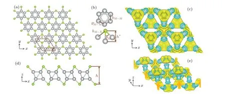
Fig.1. (a)Top view of M6X2 structure. (b)Metal nanoclusters and structural details. The green spheres represent the X atom(S,Se),the grey spheres represent the M atom(Au,Ag),and coordinates axes are marked. (c)Top view of charge density difference(Ag6Se2). (d)Side view of M6X2 structure. (e)Side view of charge density difference(Ag6Se2). The yellow area represents the accumulation of charge,the blue area represents the loss of charge,and the isosurface level is 0.004.
3.2. Stability
We calculated the cohesive energy and the phonon dispersion of theM6X2andM6XX'structures to determine their stability in terms of dynamics. The formulas for calculating the cohesive energy are as follows:


whereEtotrepresents the total energy of theM6X2orM6XX'structure.Eatomis the ground state energy of a free atom,calculated by placing an isolated atom in a large vacuum for ground state energy calculations to avoid interactions between the isolated atom and adjacent atoms. The cohesive energies of theM6X2andM6XX'structures are shown in Table 1: (Au6Se2)-3.107 eV, (Au6SSe)-3.149 eV, (Ag6S2)-2.809 eV, (Ag6SSe)-2.679 eV, and (Ag6Se2)-2.745 eV.Larger cohesive energies demonstrate higher structural stability. Because Au atoms have a stronger ability to bind electrons than Ag atoms,the absolute values of cohesive energy for the gold compounds are larger than those of the silver compounds.
To further investigate the kinetic stability of these structures, phonon dispersion was performed with the 3×3×1 supercells. Figure 2 shows no negative frequency in phonon dispersion along high-symmetry paths. In addition,the acoustic branch at theGpoint shows a linear trend, demonstrating the dynamic stability of the structures. The strong bonding betweenMandXatoms explains the stability of these materials in terms of the similar strong electron shells between Mo atoms and Au6or Ag6clusters.Moreover,the cohesive energy and phonon dispersion also illustrate the excellent stability of this system.

Table 1. Structural parameters and cohesive energy values of M6X2 and M6XX' structures(M=Au,Ag;X,X'=S,Se)after structural optimization.
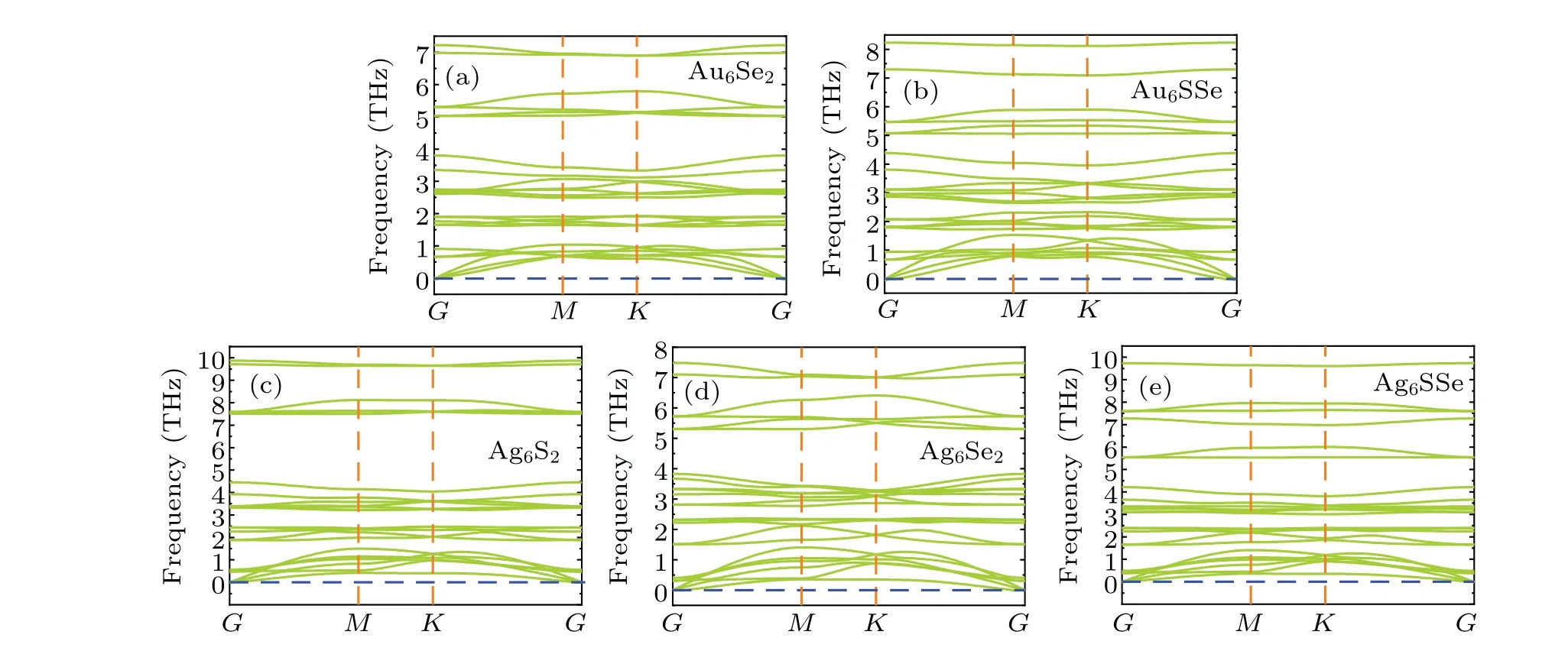
Fig.2. Phonon dispersion of M6X2 and M6XX' structures(M=Au,Ag;X,X'=S,Se)with a 3×3×1 supercell: (a)Au6Se2;(b)Au6SSe;(c)Ag6S2;(d)Ag6Se2;(e)Ag6SSe.
3.3. Band structure
Figure 3 shows the band structures ofM6X2andM6XX'(M= Au, Ag;X,X'= S, Se) calculated by the HSE06 hybridization functional. Four indirect bandgaps (Au6SSe,Ag6S2,Ag6Se2and Ag6SSe)and one direct bandgap(Au6Se2)are shown. As is well known, direct bandgaps indicate more energy conversion to effective energy with no vibration energy loss. Therefore, Au6Se2can be deemed to be an ideal candidate in optical materials. The bandgaps of the gold compounds are 1.87 eV (Au6Se2) and 1.71 eV (Au6SSe), while the bandgaps of the silver compounds are 2.61 eV (Ag6S2),2.33 eV (Ag6Se2) and 2.45 eV (Ag6SSe). Therefore, it can be concluded that the bandgaps of the gold compounds are generally larger than those of the silver compounds. The valence band maximum (VBM) and the conduction band minimum(CBM)of Au6Se2are located at pointG. The CBM of Au6SSe is located along the path of the high symmetric pointG-Min the Brillouin zone, and the VBM is located at pointG. The silver compounds(Ag6S2,Ag6Se2and Ag6SSe)have VBMs located at pointGand their CBMs are located at pointM. The bandgaps of these five materials are in the range of 1.7-2.6 eV,meaning that they are traditional narrow-bandgap semiconductor materials. The narrow-bandgap semiconductors have a wide frequency range for light absorption,demonstrating great potential for optoelectronic semiconductor devices in visible and ultraviolet light. The bandgaps of the gold compounds are within 1.7-1.8 eV, which indicates stronger absorption in the infrared region. Therefore, these gold compounds are suitable for photo-thermal conversion material. In contrast to the gold compounds, the silver compounds are more suitable for photocatalysis due to the bandgaps of approximately 2.3-2.6 eV,which are close to the redox potential of water,showing promise for water splitting applications.

Fig.3. Band structure of(a)Au6Se2;(b)Au6SSe;(c)Ag6S2;(d)Ag6Se2;and(e)Ag6SSe.
To further understand the contribution of different orbitals to the band structure of these materials as well as their electron states near the Fermi level,the total densities of states(TDOS)and partial densities of states(PDOS)of theM6X2andM6XX'structures were calculated. As shown in Fig.4,the dotted line at zero energy represents the Fermi level. The TDOS in Fig.4 exhibits sharp peaks due to the localization of transition metal d orbitals. The TDOS of the gold compounds in Figs.4(a)and 4(b)show that the contribution of the Au atoms near the Fermi level is greater than that of theXatoms. The PDOS shown in Figs.A1(a)and A2(a)demonstrate that the contributions near the Fermi level originate from the d orbitals of the Au atoms and the p orbital of theXatoms(S,Se).The localization of the gold compounds is lower than that of the silver compounds,which corresponds to the larger band width of the gold compounds shown in Fig.3. The TDOS of the silver compounds shown in Figs.4(c)and 4(d)show that the contribution of Ag in theM6X2structure matches that of theXatoms near the Fermi level but is lower than the contribution of theXatoms.This is different from the densities of states of the gold compounds. Figures A1(b),A2(b)and A2(c)show that the Fermi level originates from the d orbitals of the silver atoms and the p orbitals of theXatoms (S, Se). Due to overlapping levels near the Fermi level, the bonds between the d orbitals ofMatoms and the p orbitals ofXatoms are the dominant contribution, which is closely related to the transport properties of the materials. Near the CBM,the gold and silver compounds show similar properties,with contributions mainly from the d orbitals ofMatoms(Au,Ag)and the p orbitals ofXatoms(S,Se).
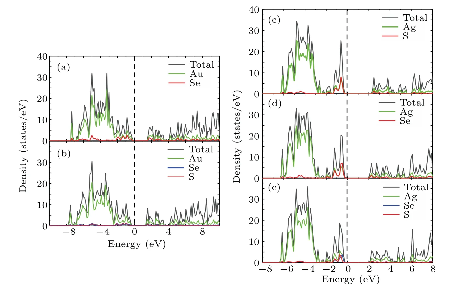
Fig.4. Densities of states of(a)Au6Se2;(b)Au6SSe;(c)Ag6S2;(d)Ag6Se2;and(e)Ag6SSe.
3.4. Photocatalytic water splitting and optical absorption
The approximate band structure can drive the redox reaction of water splitting. While the bandgaps of semiconductors influence their photocatalytic properties, the band edge positions of their VBM and CBM are also closely related to the intensity of redox reactions in photocatalytic water splitting.There are two essential steps of photocatalytic water splitting:hydrogen evolution reaction (HER) and oxygen evolution reaction(OER),which require the participation of catalysts due to the high overpotentials,dynamic barrier and low efficiency of four electrons involved in the reaction.[45-48]Under the light irradiation, photoexcited electrons and holes are produced to participate the whole reaction.[49-51]Figure 5 shows the process of photocatalytic water splitting. When CBM is higher than the reduction potential(HER:4H++4e-→2H2)of water splitting and VBM is lower than the oxidation potential(OER:2H2O→O2+4H++4e-),[52]there will be an active force driving the redox reaction. As a result,the H2 evolution and O2 evolution proceed. The reaction activity of catalytic water splitting is closely related to the band edge position.
Band edge position calculations are based on Mulliken electronegativity theory.[53,54]Formulas (3) and (4) are used to calculate the band edge positions of the conduction band(ECB)and the valence band(EVB)
The calculated values ofEa(M),Ea(X), andEa(X') are the electronegativity values of theM,X,andX'atoms,which can be measured by experiments.[61]Mulliken electronegativity is equal to the geometric mean of electron ionization potential and electron affinity. Methods for calculating band edge positions are a major research focus.[62-64]The electronegativity values of the atoms used in these calculations are Ag(4.40 eV), Au (5.77 eV), Se (7.02 eV), and S (7.43 eV).[61]The VBM and CBM band edge positions were determined by aligning with the relative standard hydrogen electrode potential,and these band edge positions are shown in Fig.6(a). The redox potential of water splitting lies between the band edges of the silver compounds(Ag6X2and Ag6XX'(X,X'=S,Se)),revealing their photocatalytic water splitting potential. However, this is only a theoretical prediction based on the band edge position of these materials, and real aqueous environments may involve other requirements. Therefore,further theoretical and experimental study is needed.[65]
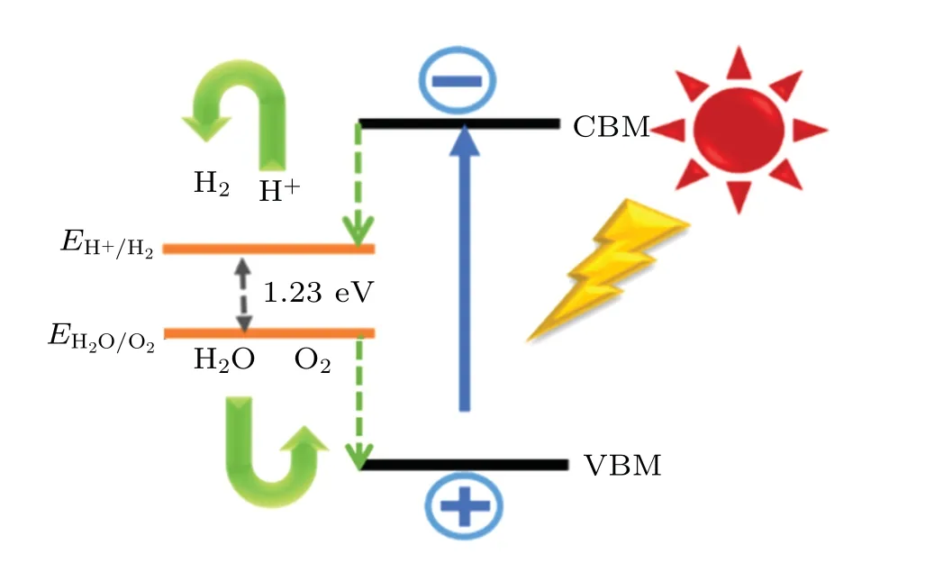
Fig.5. The mechanism of photocatalytic water splitting.
The energy range of light absorption is a crucial factor for the performance of optoelectronic device materials. Therefore, the absorption coefficient is a significant parameter for characterizing the optical properties of materials, and outstanding optical materials have high absorption coefficients.The absorption spectra of two-dimensional materials are calculated by in-plane polarized light excitation, and the dielectric constants are obtained by the HSE06 exchange-correlation potential method.The dielectric coefficient determined by frequency includes a real part and an imaginary part. Therefore,calculating the absorption spectrum of a material related to photon energy is as follows:[66]
The light absorption of the fiveM6X2andM6XX'structures is shown in Fig. 6(b). The absorption coefficients of these materials are as high as 3×105cm-1and their absorption peaks are located in the visible light range(1.7-3.3 eV),meeting the requirements of photocatalytic water splitting. In addition,the resonance modes in the high-energy region are also strong absorption peaks. In the visible region, Au6Se2has two obvious resonance absorption peaks at about 2.25 eV and 3.2 eV,while Au6SSe has three resonance absorption peaks at about 2 eV, 2.5 eV, and 3.2 eV. Ag6Se2has two resonance absorption peaks at about 2.6 eV and 3 eV,while Ag6S2and Ag6SSe each only demonstrate one resonance absorption peak at about 3.2 eV and 3 eV, respectively. In the high-energy ultraviolet region, the resonance absorption peaks of the five structures are in the range of 4-4.5 eV.The gold compounds have more resonance absorption peaks and higher absorption coefficients in the visible light region. Therefore, compared with the silver compounds, the gold compounds have higher absorption efficiency and activity under visible light. Among the silver compounds,Ag6Se2has the highest number of resonance absorption peaks, meaning that it is the most suitable material for photocatalytic water splitting in the visible light region.

Fig.6.(a)Band edge positions of M6X2 and M6XX'structures(M=Au,Ag;X,X'=S,Se),where the black dotted line represents the standard redox potentials for water splitting. (b)Absorption spectra of M6X2 and M6XX'structures,where the area surrounded by the black dotted line is the energy range of the visible region.
3.5. Tuning band structures and optical property by biaxial strain
Strain engineering is an effective strategy for regulating the electrical, optical, topological, and thermoelectric properties of semiconductors. In many practical material syntheses, generated single-layer crystals and heterostructures will produce stress and strain due to their synthesis conditions and environments,and strain modulation also occurs in some practical applications. However, using strain effects to optimize the geometric structures and properties of materials and meet the requirements of microelectronic devices, optoelectronic devices, and solar cells is always a challenging subject. The use of uniform biaxial strain is more effective than uniaxial strain or shear strain for regulating the bandgap of semiconductors.[67]Therefore,uniform biaxial strain(including tensile strain and compressive strain)was applied to adjust the electronic structure and optical properties of theM6X2andM6XX'materials in this paper. A biaxial stress field was simulated by fixing the lattice constantaunder strain. The original optimized lattice constant isa0,and the degree of biaxial strainηwas determined with the equationη=(a-a0)/a0. A biaxial strainηrange from-6%to 6%was examined with a step size of 2%. Positive values represent the tensile strain, while negative values represent the compressive strain.
To explore the stability of theM6X2andM6XX'structures under strain regulation, the curves of cohesive energy under different strains were obtained, as shown in Fig. 7(a).As shown, the cohesive energy values depend on the biaxial strainη.Although the absolute value of cohesive energy gradually decreases with increasing strain,it remains high enough to demonstrate high stability under all the examined tensile strain and compressive strain values. Figure 7(a) shows that the cohesive energy under tensile strain decreases more slowly than that under compressive strain. Therefore,under the same strain,these structures are more stable under tensile strain.
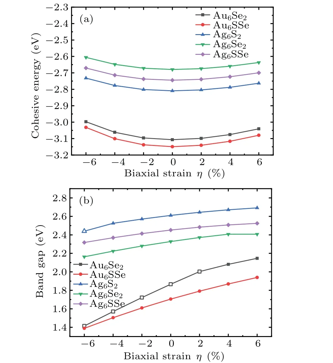
Fig. 7. (a) Cohesive energy of M6X2 and M6XX' structures (M=Au,Ag; X,X' =S, Se) under biaxial strain. (b) Bandgaps of M6X2 and M6XX' structures under biaxial strain. The solid symbol represents the indirect bandgap and the hollow symbol represents the direct bandgap.
Figure 7(b)shows the bandgap variation of theM6X2andM6XX'materials under biaxial strain. The bandgap gradually decreases with increasing compressive strain. In contrast,the bandgap gradually increases with increasing tensile strain. An almost quasi-linear trend is seen, demonstrating potential use in sensors and high-precision devices. Interestingly, when a tensile strain is applied(η=4%),the Au6Se2direct bandgap transitions to an indirect bandgap, and when a compressive strain is applied(η=-6%),the Ag6S2indirect bandgap transitions to a direct bandgap.
To further study the mechanism of direct-indirect bandgap transition with biaxial strain, the projected bands of Au6Se2under different strains (η=0%, 4%) were determined,as shown in Figs.8(a)and 8(b)with the contributions of the Au and Se orbitals. The bands are shown relative to the CBM at twok-points (GandB). With no biaxial strain, the VBM and CBM of Au6Se2are both located at pointG. However,when compressive strain is applied(η=4%),the CBM shifts from pointGto pointB, which is located on theG-Mpath. Therefore, the direct bandgap transitions to an indirect bandgap.Figure 8(c)shows that when tensile strain is applied,the contribution of Au d and p orbitals decreases and the contribution of Au s orbitals increases at both pointsGandB.The contributions of Se atoms do not significantly change under different strains,so they are not shown in Fig.8(c). When compressive strain is applied,the opposite trend is seen.Overall,the Au s electrons at pointGand pointBchange at a similar rate. The contribution of Au d electrons only slightly and insignificantly varies. For the electron-occupied state of the Au p orbital(shown with bold red lines),the rate of variation at pointGis obviously higher than that at pointB. Therefore,the CBM level at pointGchanges more rapidly than at pointB(Figs.8(a)and 8(b)). This leads to the direct-indirect bandgap transition. However, further research on this transition is required.

Fig.8. (a)Projected band of Au6Se2 with Au atom and Se atom contributions under the strain η =0%. (b)Projected band of Au6Se2 with Au atom and Se atom contributions under the strain η =4%. (c)Contribution of orbitals to the projected bands.
Moreover, we perform the projected band structures under different strains (η= 0,-6%) and the contribution of orbitals for Ag6S2to explore the explanation of the indirectdirect bandgap transition under biaxial strain. As shown in Figs.9(a)and 9(b)relative to the CBM at twok-points(G,M),with no biaxial strain,the VBM of Ag6S2is located at point G and the CBM is located at pointM. When compressive strain is applied (η=-6%), the CBM of Ag6S2shifts from pointMto pointG, resulting in the transition between a direct and indirect bandgap. Figure 9(c) shows that under compressive strain, the contributions of Ag d and Ag p orbitals increase and the contribution of Au s orbitals decreases at both pointsGandM.The projected orbital contributions of the S atoms do not significantly change with changing strain, so they are not shown in Fig.9(c).When tensile strain is applied,the opposite trend is seen. Overall,the Ag s orbital contributions at pointsGandMchange at the same rate. The contribution of the Ag d orbital varies at a similar rate at pointsGandB. The variation rate of the contribution of the Au p orbital(shown with bold red lines)is higher at pointGthan at pointM. Therefore,the CBM level changes more rapidly at pointGthan at pointM(Figs. 9(a) and 9(b)), which results in the indirect-direct bandgap transition.
Figure 10 shows the optical absorption of theM6X2andM6XX'structures under different biaxial stains. Biaxial strain has a strong regulating effect on the optical absorption of these materials. With increasing compressive strain, the resonance absorption peak in the visible region redshifts,consistent with the decreasing bandgap shown in Fig.7(b).In contrast,the resonance absorption peak blueshifts in the visible region. This is related to the increasing bandgap under increasing tensile strain shown in Fig.7(b). It is worth noting that the intensity of the resonance absorption peak in the visible region gradually increases under increasing strain. This demonstrates the high solar energy utilization efficiency of these materials for photocatalytic water splitting applications.

Fig.9. (a)Projected band of Ag6S2 with Ag atom and S atom contributions under a strain of η =0%. (b)Projected band of Ag6S2 with Ag atom and S atom contributions under a strain of η =-6%. (c)Contribution of orbitals to the projected bands.

Fig.10. Optical absorption of M6X2 and M6XX'structure for biaxial strain(M=Au,Ag;X,X'=S,Se): (a)Au6Se2;(b)Au6SSe;(c)Ag6Se2;(d)Ag6S2;(d)Ag6SSe.
4. Conclusion
In conclusion,M6X2andM6XX'structures(M=Au,Ag;X,X'=S, Se) were studied by DFT theoretical calculations based on first-principles theory.The high stability of these materials was predicted by investigating phonon dispersion and cohesive energy. Of these materials,one has a direct bandgap(Au6Se2) and four have indirect bandgaps (Au6SSe, Ag6S2,Ag6SSe, and Ag6Se2). The band edge positions and optical absorption coefficients of the Ag compounds demonstrated the great potential for photocatalytic water splitting. Furthermore, the bandgaps and optical properties of these materials were regulated by biaxial strain. Their cohesive energy illustrates their stability under strain. Intriguingly, a quasi-linear bandgap trend and a direct to indirect bandgap transition were found under biaxial strain. To further explore this mechanism,projected bands were determined to investigate the changes of orbital contributions under strains that led to the band edge variation. Finally, the optical absorption coefficients of the structures under biaxial strain were obtained. The resonance absorption peak blueshifts and redshifts under tensile strain and compressive strain, respectively. Overall, this paper provides a meaningful idea and method for exploring new twodimensional nanomaterials with great potential in microelectronic,optoelectronic,and photocatalytic applications.
Appendix A
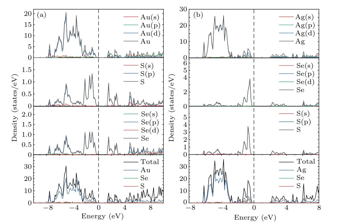
Fig.A1. PDOS of(a)Au6SSe and(b)Ag6SSe.

Fig.A2. PDOS of(a)Au6Se2;(b)Ag6S2;and(c)Ag6Se2.
Acknowledgements
Projected supported by the National Natural Science Foundation of China (Grant No. 11974253), the National Key R&D Program of China (Grant No. 2017YFA0303600),and Science Specialty Program of Sichuan University (Grant No.2020SCUNL210).
猜你喜欢
中国水土保持(2022年7期)2022-07-14
贵州开放大学学报(2022年1期)2022-04-18
小小说月刊·下半月(2022年3期)2022-03-17
小小说月刊(2022年6期)2022-03-16
今日农业(2021年17期)2021-11-26
今日农业(2021年17期)2021-11-26
音乐天地(音乐创作版)(2019年6期)2019-09-20
今日农业(2019年15期)2019-09-03
领导决策信息(2017年14期)2017-06-21
阅读(中年级)(2009年5期)2009-06-23
- Chinese Physics B的其它文章
- Characterizing entanglement in non-Hermitian chaotic systems via out-of-time ordered correlators
- Steering quantum nonlocalities of quantum dot system suffering from decoherence
- Probabilistic quantum teleportation of shared quantum secret
- Spin–orbit coupling adjusting topological superfluid of mass-imbalanced Fermi gas
- Improvement of a continuous-variable measurement-device-independent quantum key distribution system via quantum scissors
- An overview of quantum error mitigation formulas