
Superconductivity and unconventional density waves in vanadium-based kagome materials AV3Sb5
2022-09-24 08:02HuiChen陈辉BinHu胡彬YuhanYe耶郁晗HaitaoYang杨海涛andHongJunGao高鸿钧
Chinese Physics B 2022年9期
Hui Chen(陈辉) Bin Hu(胡彬) Yuhan Ye(耶郁晗) Haitao Yang(杨海涛) and Hong-Jun Gao(高鸿钧)
1Institute of Physics and University of Chinese Academy of Sciences,Chinese Academy of Sciences,Beijing 100190,China
2CAS Center for Excellence in Topological Quantum Computation,Beijing 100190,China
3Songshan Lake Materials Laboratory,Dongguan 523808,China
Keywords: kagome metal,superconductivity,charge density wave,pair density wave
1. Introduction
Kagome lattice,[1]which is recognized as a sister to the more common hexagonal tiling of graphene, stands out as a model system for the genesis of unconventional electronic and magnetic properties.[2]The kagome lattice can be roughly categorized into the insulating and (semi-)metallic materials.The latter one, especially the transition-metal kagome materials, are of increasing interest due to their potential to manifest non-trivial topologies and unique electronic structures. In most transition-metal kagome lattice materials,the transitionmetal elements occupy the vertices of the two-dimensional networks of corner-sharing triangles [Fig. 1(a)]. In contrast to the strongly correlated insulating kagome compounds such as the Herbertsmithite for quantum spin liquids and doped Mott insulators where the geometrical frustration of antiferromagnetic order plays a dominant role,[2-6]these transitionmetal compounds are usually correlated metals with itinerant electrons. From the perspective of band theory, the transition-metal kagome materials possess Dirac points and nearly flat bands that naturally promote topological and correlation effects,providing exciting opportunities for exploring frustrated, correlated, and topological quantum states of matter. Remarkable correlated topological phenomena,including massive spin-polarized Dirac fermions,[7-9]magnetic Weyl semimetal,[10-12]topological Chern magnet,[13]negative flat band orbital magnetism,[14]large anomalous Hall effect[15]and spin-orbit polarons,[16]have been observed in the class of Fe-,Co-,and Mn-based magnetic transition-metal kagome shandites[Fig.1(a)].
Recently, a new family of vanadium-based kagome metalsAV3Sb5(A=K,Rb,and Cs)has been discovered by Wilson’s group.[17]AV3Sb5unit cell belongs to the space group ofP6/mmm(No. 191) and is consisted of a sandwich stacking layerA-Sb2-VSb1-Sb2-A, where alkali metalAforms the hexagonal lattice, Sb2 atoms constitute a honeycomb lattice and Sb1 atoms construct a hexagonal lattice with each Sb1 atom surrounded by six V atoms which are laying on the kagome lattice [Fig. 1(a)]. Due to the unique kagome geometry,theAV3Sb5was predicted to hostZ2nontrivial topological band structures by calculations based on the density functional theory (DFT).[18]Figure 1(b) shows the typical magnetization and heat capacity characterizations of a CsV3Sb5single crystal.[18,19]The magnetization and specific heat capacity measurement suggest that all materials in theAV3Sb5family exhibit a phase transition at 80-110 K, which corresponds to the charge density wave(CDW)transition. Another phase transition at a lower temperature of 0.9-3 K implies the superconducting(SC)condensation.[18-20]
It is more intriguing that these materials are nonmagnetic but exhibit giant anomalous Hall effect (AHE)at low temperature.[21]Unconventional charge orders that break the time-reversal symmetry[22-24]and proximityinduced spin-triplet pairing pointing to an unconventional superconductivity[25,26]have been recently reported. Aside from the evidence for gap nodes and non-trivial core states in magnetic-field induced vortices, the nature of the SC ground state with strong coupling and its correlation to the CDW states have also been reported.[27-29]Moreover, the pair density wave (PDW) was demonstrated with a roton-like behavior and served as a “mother state” corresponding to the pseudogap.[19]
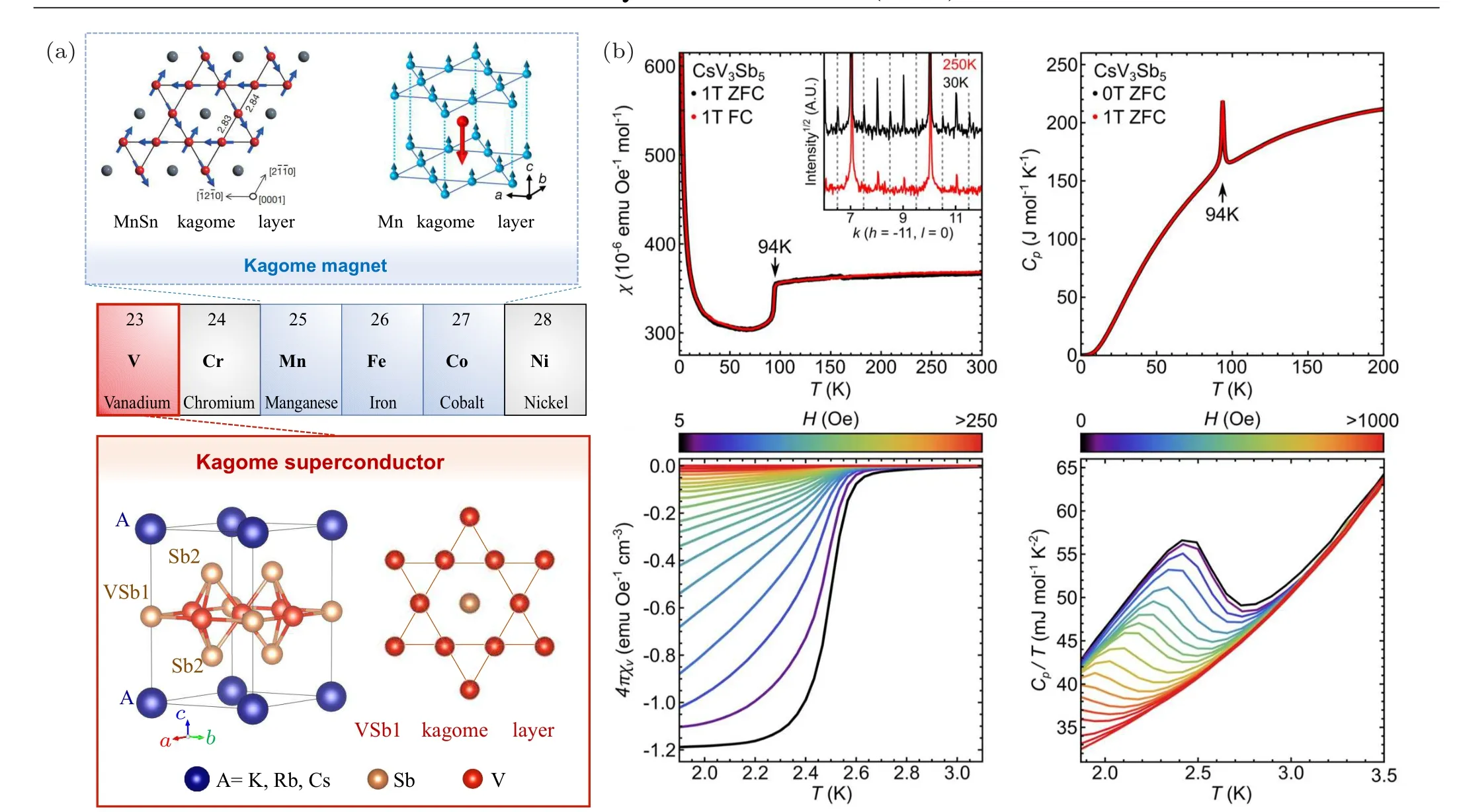
Fig.1. Discovery of superconductivity and charge density waves in kagome metal AV3Sb5. (a)Some elements of transition metals in the periodic table. The Mn-,Fe-and Co-based kagome metals normally host magnetic ground states(the magnetic orders in exemplary MnSn kagome layer in Mn3Sn[15] and Mn kagome layer in TbMn6Sn6 [13] are shown in the upper panel),while the V-based kagome metals are found to host superconducting ground states,featuring a kagome superconductor. The atomic models of AV3Sb5 and VSb1 kagome layer are shown in the bottom panel. (b)The magnetization and heat capacity measurements of CsV3Sb5, showing that the critical temperature of CDW is about 94 K and the critical temperature of superconductivity is about 2-3 K.Adapt with permission from Ref.[18].
In this review, we will focus on the recent studies on the unconventional density waves and superconductivity ofAV3Sb5. Firstly, we introduce the observations of the AHE,which establish the exploration for the hidden time-reversal symmetry-breaking states. Subsequently,we review the studies of CDWs inAV3Sb5including the 2×2×2(4) charge orders in the bulk and unidirectional stripe charge orders observed at Sb surface. The anomalous features including absence of phonon anomaly, rotation symmetry breaking and time reversal symmetry breaking are discussed. Next, we briefly summarize the studies of superconductivity and topological band structures. The competition between superconductivity and CDWs by changing the pressure,chemical doping, thickness, and strain is also presented. Finally, we illustrate the spectroscopic evidence of pair density wave (PDW)state with non-trivial features, promoting further understanding of the similar phenomenon in the cuprates and other superconductors.
2. Emergent giant anomalous Hall effect in AV3Sb5
AHE[30-33]is one of the hot topics in the field of condensed matter physics due to its fundamental research interest and exciting applicational prospects. In principle, AHE can be categorized into intrinsic AHE which is mainly induced by the Berry curvature,and extrinsic AHE which is governed by the electrons scattering in the periodic potential of a crystal.The magnetic kagome materials[32-34]due to their bulk gap accompanying the dissipationless edge state, which can contribute to the Berry curvature, are triggering enough research interests in the seeking of AHE,and the typical examples are Co3Sn2S2,[32]CoMnGa,[35]and GdMn6Sn6.[33]More interestingly, theAV3Sb5has been proven to also possess giant AHE[21,36,37]but without magnetic moment.[38]
When performing Hall measurement below the CDW transition temperature, anomalous Hall conductivity can be detected[21,36][Figs. 2(a) and 2(b)]. Figure 2(c) collects the anomalous Hall properties of more than ten kinds of materials and is divided into three regions depending on the value of longitudinal conductivityσxx. There are some intriguing features in these results. Firstly, both KV3Sb5and CsV3Sb5show quadratic behavior ofσAHEversusσxx, and the maximal anomalous Hall conductivity can reach as high as~15507 Ω-1·cm-1for KV3Sb5,[36]and~21000 Ω-1·cm-1for CsV3Sb5,[21]which exceed most of the materials discovered before, showing the discovery of giant AHE without ferromagnetic ordering for the first time in theAV3Sb5family.Secondly,both KV3Sb5and CsV3Sb5are located in similar positions, demonstrating the possible same origin of AHE in theAV3Sb5family. Finally,the experimental anomalous conductivity is much higher than the theoretical calculation value[39]when mainly considering the intrinsic Berry curvature effect,indicating that the dominant role to control the AHE is the skew scattering. However, Yuet al.[21]pointed out that the paramagnetic impurities are about 0.7%. It is still unclear how such low amount of impurities induce the giant anomalous Hall conductivity. On the other hand, Kenneyet al.[38]claimed that there are no local moments in KV3Sb5, directly challenging the skew scattering scenario.In addition,the AHE was found to concurrent with CDW,[21,36,37]which indicates that the mechanism of the AHE is beyond the proposed skew scattering. The discovery of giant anomalous Hall effect starts the exploration for the time-reversal symmetry-breaking states inAV3Sb5.

Fig. 2. Giant anomalous Hall effect observed in AV3Sb5. (a) AHE in KV3Sb5 (adapted from Ref. [36]). (b) AHE in CsV3Sb5 at various temperatures (adapted from Ref. [21]). (c) σAHE versus σXX for a variety of materials comparing with CsV3Sb5 spanning various regimes from localized hopping regime to the skew scattering regime. For CsV3Sb5, σAHE follows quadratic scaling only at low temperature and locates at the same position with K1-xV3Sb5 (adapted from Ref.[21]).
3. Unconventional charge density wave in AV3Sb5
The strong correlation between AHE and CDW raises the questions: what is the origin of the charge orders? Is the time reversal symmetry breaking in the charge orders?
In the situation of one dimension, CDW originates from the combination of electron-phonon coupling and Fermi surface nesting,namely,Peierls distortion.[40]When considering the existence of electron-electron correlations,multiple bands,and spin-orbit coupling in the situation of two or three dimensions,the mechanism of CDW becomes more complex.[41-44]The CDWs inAV3Sb5family exhibit multiple intriguing behaviors with unconventional origins.
3.1. The 2×2 superlattice charge orders in kagome lattice
The phase transition at a critical temperatureT∗ranging from 78 K to 103 K is attributed to the CDW phase transition inAV3Sb5.The formation of 2×2 superlattice charge order in kagome lattice is firstly evidenced by the early x-ray diffraction(XRD)experiments where the faint superlattice peaks appear at half integer positions below the CDW transition acrossT∗.[18]
To further study the 2×2 superlattice, low-temperature scanning tunneling microscopy (STM) is applied due to the atomically-precise visualization of the electronic order both in real space and reciprocal space. The CDW transition with 2×2 superlattice modulations is observed by using STM at the temperature belowT∗. Figure 3 shows the typical STM results of CsV3Sb5. As shown in Figs. 3(a) and 3(b), the Fourier transform of STM topography obtained at Sb surface shows six bright intensity points located at half Bragg reciprocal lattice vectors, directly evidencing the existence of 2×2 charge order in the atomic scale. In general, CDW as the spatial charge density modulation is more relevant to the density of state, which is equivalent to differential conductance maps. And the Fourier transforms of the differential conductance(dI/dV)maps[Fig.3(c)]show that the 2×2 CDW persists from-300 mV to 200 mV,and show the non-dispersive features.[45]Although STM measurement is performed at the Sb layer,the 2×2 CDW is thought to originated from the underlying kagome lattice as the Sb electronic state contributes little to the charge ordering and tunneling process.[46]Moreover,the temperature-dependent dI/dVspectra exhibits a gap of~20 meV enduring to 78 K and gapless concomitant with the disappearance of 2×2 CDW at 106 K, linking to theT∗of 94 K. Following the discovery of 2×2 charge orders in CsV3Sb5, 2×2 CDWs are also evidenced by the Fourier transform of STM topography in KV3Sb5[39]and RbV3Sb5[Fig.3(d)].[23]
The observations of 2×2 superlattice at Sb surface immediately raise a question:whether the CDW modulates along thec-axis. Lianget al.[47]revealed a three-dimensional (3D)2×2×2 charge order by analyzing the phase information of the CDWs across the single-unit-cell surface step between two neighboring Cs layers. When focusing on the arrangement of Cs atoms,aπ-phase shift between 2×2 CDWs appears to distinguish up and down layers[Fig.3(e)],suggesting a 2×2×2 CDW in three dimensions. Following the STM observations,the existence of 2×2×2 CDW in the bulk has been further confirmed by many other characterizations.[17,48-51]The CDW peak at half integerLin the XRD measurements proves that the CDWs form a 3D 2×2×2 superstructure[Figs.4(a)and 4(b)].[17,50]It should be worthy to mention that, both the 2×2×2 CDW[50]and the 2×2×4 CDW for the bulk material[52]have been observed.Very recently,the coexistence of 2×2×2 and 2×2×4 CDW orders was proposed from angle-resolved photoemission spectroscopy(ARPES)measurements.[53]
Both the electron-electron coupling and electron-phonon coupling play a role in the formation of CDW. The Fermi surface displayed combing with the existence of von Hove singularity near theMpoint[54-56]can satisfy the nesting scenario and give strong indication to form a 2×2×2(4)CDW which breaks the translational symmetry in the lattice[Fig.4(c)].[18,52,57]The quantum oscillation measurements on CsV3Sb5evidence that the CDW invokes a substantial reconstruction of the Fermi surface pockets associated with the V orbital and kagome lattice framework.[52]The absence of phonon anomaly in the XRD results [Figs. 4(d) and 4(e)]at the temperature below and beyondT∗implies that the CDW is related to the electron-electron correlation and weak electron-phonon coupling.[50]However, ARPES,[58]optical spectroscopy[59]and the neutron scattering[60]measurements demonstrate that the wave-vector-dependent electron-phonon coupling plays an important role in the CDW order. In addition,recent Raman spectroscopy reported the anomalous amplitude modes in the absence of soft phonons, indicating that the CDW exhibits the character of strong electron-phonon coupling.[61]In the phonon spectroscopy,the structural change shows a predominately first-order phase transition. No CDW amplitude mode is identified in the ordered phase.[62]Similarly, the nuclear magnetic resonance spectroscopy (NMR)measurements show a first-order structural phase transition associated with orbital ordering and a typical second order transition behavior in quadrupole splitting belowTCDW.[49,63]These results suggest an unusual coupling between the electron and lattice degrees of freedom, which is different from the traditional CDW condensate.
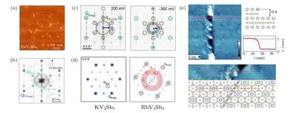
Fig.3. The 2×2 superlattice charge orders in the kagome lattice of AV3Sb5. (a),(b)STM image and corresponding Fourier transform obtained at the Sb surface of CsV3Sb5,showing the 2×2 superlattice charge order(adapted from Ref.[19]). (c)Fourier transform of dI/dV map at distinct energy showing the dispersive 2×2 charge order(adapted from Ref.[45]). (d)Observation of 2×2 superlattice at the Sb surface of KV3Sb5 (adapted from Ref.[39])and RbV3Sb5 (adapted from Ref.[23])(e)Illustration of three-dimensional 2×2×2 CDW near a single-unit-cell(adapted from Ref.[47]).
ARPES measurements reveal complex band structures related to the CDWs. Except for the rich nature of the von Hove singularity,[54-56]the CDW induced band renormalization and energy gaps are observed.[64]The CDW gap shows distinctive momentum dependent features[Fig.4(f)].[57,58,65]
To understand the anomalies in the experimental studies of the 2×2 superlattice charge order inAV3Sb5, there are also some theoretical works on its mechanism. For example, Tanet al.[46]found that the pristine lattice structure ofAV3Sb5[Fig.5(a)]is not stable due to the softening acoustic phonon modes at the Brillouin zone boundary nearMandLpoints[Fig.5(d)for CsV3Sb5]. When considering an in-plane 2×2 modulation of the star of David[SD,Fig.5(b)]or the inverse star of David[ISD,Fig.5(c)],the imaginary phonon frequency near theMpoint can be extremely reduced[Figs.5(e)and 5(f)]. And further including a 2×2×2 reconstruction,theL-point soft mode can be removed as well.The 2×2×2 structure is in agreement with the experimental results.[50]Moreover,all three components in theAV3Sb5family show reduced total energy for SD and ISD structures, and the ISD phase hosts even lower energy than the SD phase [Figs. 5(g)-5(i)].At the same time,the ISD phase agrees better with experimental results in diffraction pattern,[18]STM image,[39]and transient reflectivity results[48]than the SD phase. Recent ARPES measurements indicate the coexistence of SD and ISD patterns in theAV3Sb5.[66]Although many scenarios for the origin of CDWs are proposed by various theoretical works,[46,67-69]the formation mechanisms of the charge orders are still unclear.

Fig.4. Unconventional CDW in AV3Sb5. (a)Temperature-dependent CDW peaks of RbV3Sb5 at Q=(3.5,0,0). (b)Temperature-dependent Raman spectra on CsV3Sb5 from 150 K to 3 K. The black dots mark the peak positions of the continuum near 19 meV. (c) Fermi-surface map of RbV3Sb5 measured at photon energies of hν =90 eV corresponding to kz=π and 0.15π around the ¯M point. Data are taken at T =15 K.(d),(e)The IXS determined LA of RbV3Sb5 along Γ(3,0,0)to M(3.5,0,0)at temperatures of T =300 K and 50 K,where(d)is the extracted-temperature-dependent phonon dispersions from(e)(adapted from Ref.[50]). (f)Three-dimensional plot of the Fermi surface-dependent and momentum-dependent CDW gaps in KV3Sb5 (adapted from Ref.[58]).
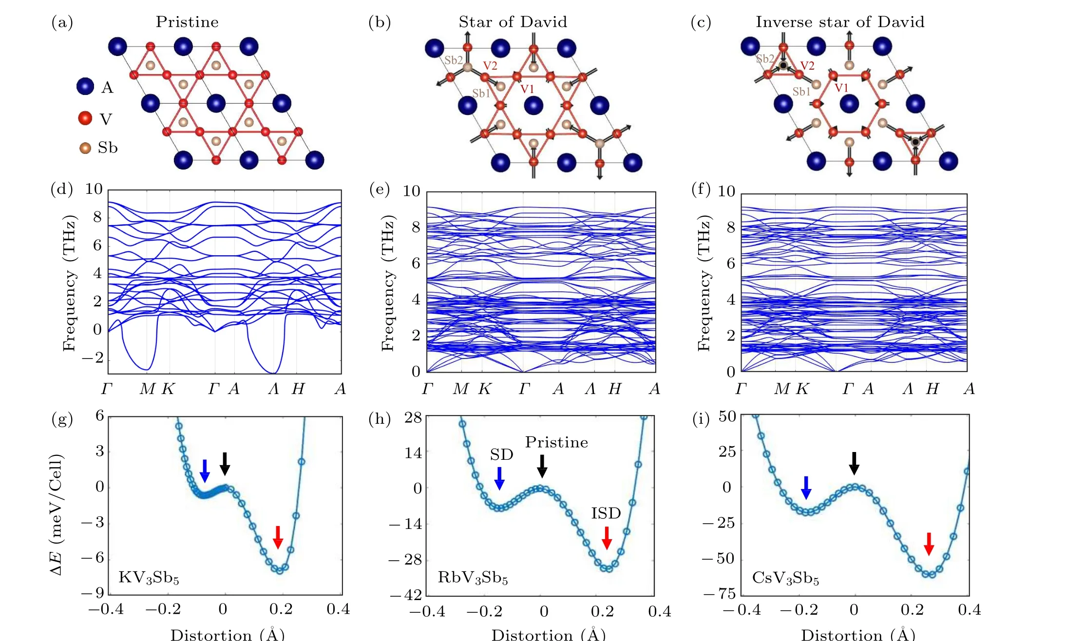
Fig. 5. DFT calculation. Crystal structures of KV3Sb5 in the pristine phase, the star of David 2×2 CDW phase, and the inverse star of David phase. Corresponding phonon dispersions are shown in the lower panels. A 2×2 supercell is shown in (a). Imaginary (negative) phonon frequency in (d) corresponds to the breathing mode of the kagome lattice. Such a breathing instability is related to CDW distortions. The breathing out and breathing in lead to two different structures in (b) and (c), where the red arrows indicate the lattice distortion due to the breathing mode. In CDW phases, V1 and V2 represent inequivalent vanadium sites of the kagome lattice, and Sb1 and Sb2 are inequivalent sites of the honeycomb lattice. (g)-(i) Total energy profiles for the three compounds:KV3Sb5,RbV3Sb5,CsV3Sb5,respectively. The distortion stands for the amplitude of the breathing-phonon mode where the negative values are used for star of David(SD)in order to distinguish from inverse star of David(ISD).The ΔE stands for the relative total energy with respect to the pristine phase per supercell(36 atoms). Spin-orbit coupling is considered(adapted from Ref.[46]).
3.2. Rotation symmetry breaking charge orders
In addition to the modulation ofcaxis for the charge orders, the 2×2 superlattice in the kagome lattice is found to show rotation-symmetry-breaking features. In the Raman measurements,the symmetry is reduced fromC6toC2,[48]indicating that three CDW directions are not identical. Liet al.found that one of the CDW directions is distinctly different compared with the other two in the Fourier transform of STM topography obtained at the Sb surface of KV3Sb5, indicating an intrinsic rotation-symmetry-broken electronic ground state[Fig.6(a)].[70]Moreover,STM results on the 1×1 Cs surface suggest that the 2×2 CDW breaks the intra-unit-cell rotational symmetry,leading to the electronic nematicity[Fig.6(b)].[51]This unique two-fold symmetry of the 2×2 CDW arises when temperature below~40 K, indicating the possible introduction of interlayer coupling.[51,71]
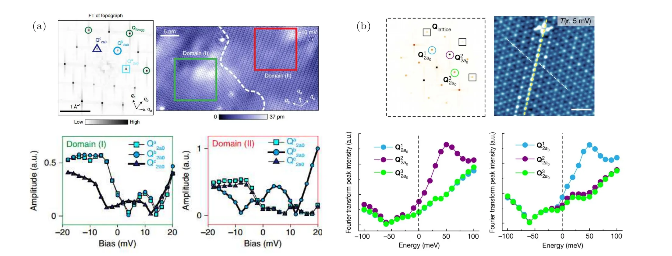
Fig. 6. Rotation symmetry breaking of CDWs. (a) Observation of rotation symmetry breaking 2×2 CDWs at the Sb surface of KV3Sb5 (adapted from Ref.[70]). (b)Observation of 2×2 CDWs driven nematicity at the Cs surface of CsV3Sb5 (adapted from Ref.[51]).
Besides the rotation symmetry breaking 2×2 CDW inAV3Sb5family, another symmetry breaking order, a featured stripe charge order,is also observed.AlthoughAV3Sb5family share the same crystal structure,the 4a0charge order is mainly observed on the Sb surface of Rb and Cs compounds instead of K compound[19,23,25,39,45]by low-temperature STM,as shown in Figs.7(a)-7(c). This special charge order can persist to surface defects and step edge[72][Fig.7(d)]and occasionally extend to 5a0[Fig.7(a)].During the process of imaging in STM,it is found that this 4a0stripe can be shifted withπphase along the scanning direction[Fig.7(a)],leading to the possibility of CDW engineering.[73,74]
Zhaoet al.,[45]have systematically investigated the 4a0charge “stripe” modulation and anisotropic quasiparticle interference on the Sb surface of CsV3Sb5. There are several significant signals of the 4a0CDW in the Fourier transform[Fig. 7(e)]. Firstly, the 4a0CDW can only exist below the temperature of~60 K,giving its transition temperature. Secondly, its Fourier transform wave vector has a small deviation from the commensurate 4a0period because of the phase slips. Finally, similar to the 2×2 CDW, 4a0peaks are nondispersive, and thus consistent with the behavior of CDW. In addition, the domain boundary between 4a0CDWs has also been discovered, which further supports the intrinsicality of the rotation symmetry breaking of 4a0CDW, as observed by different STM groups.[19,45]
It is worth noting that the as-obtained large Sb surface usually appears after a special“sweep process”by moving the alkali atoms aside.[19,45]The stripe charge order was only observed on the Sb surface by STM up to now.Different research groups raised the debate whether the 4a0charge order is a surface effect[75]or complex bulk effect.[19,48,76]The origin of the rotation symmetry breaking of the 4a0stripe order as well as the 2×2 CDW needs more experimental evidence and theoretical understanding.
3.3. Time-reversal symmetry-breaking charge order
Since the discovery of the AHE in KV3Sb5,[36]muon spin spectroscopy results claim that there is no observable local moment in such material.[38]Subsequently,an STM group from Princeton University[39]inspected the time-reversal symmetry breaking in KV3Sb5by studying the magnetic field response of the 2×2 CDW. Their main results are shown in Fig. 8(a), which consist of three images as the Fourier transforms of STM spectroscopic maps at different magnetic field environments. When the magnetic field is outside the system,the spectroscopic data shows intensity anisotropy at three different directions, and these 2×2 CDW vector peaks are in order clockwise from the lowest to the highest. By introducing a magnetic field, the chirality of 2×2 CDW can be switched from clockwise to anti-clockwise, implying that the 2×2 CDW breaks the time-reversal symmetry. The chiral property of the 2×2 CDW is claimed to exist on the Sb surface of RbV3Sb5[23]and CsV3Sb5[75]as well. Most recently,the time-reversal symmetry breaking (TRSB) bounded to the CDW has been evidenced by the muon spin relaxation/rotation experiment as well[Fig.8(b)].[24]
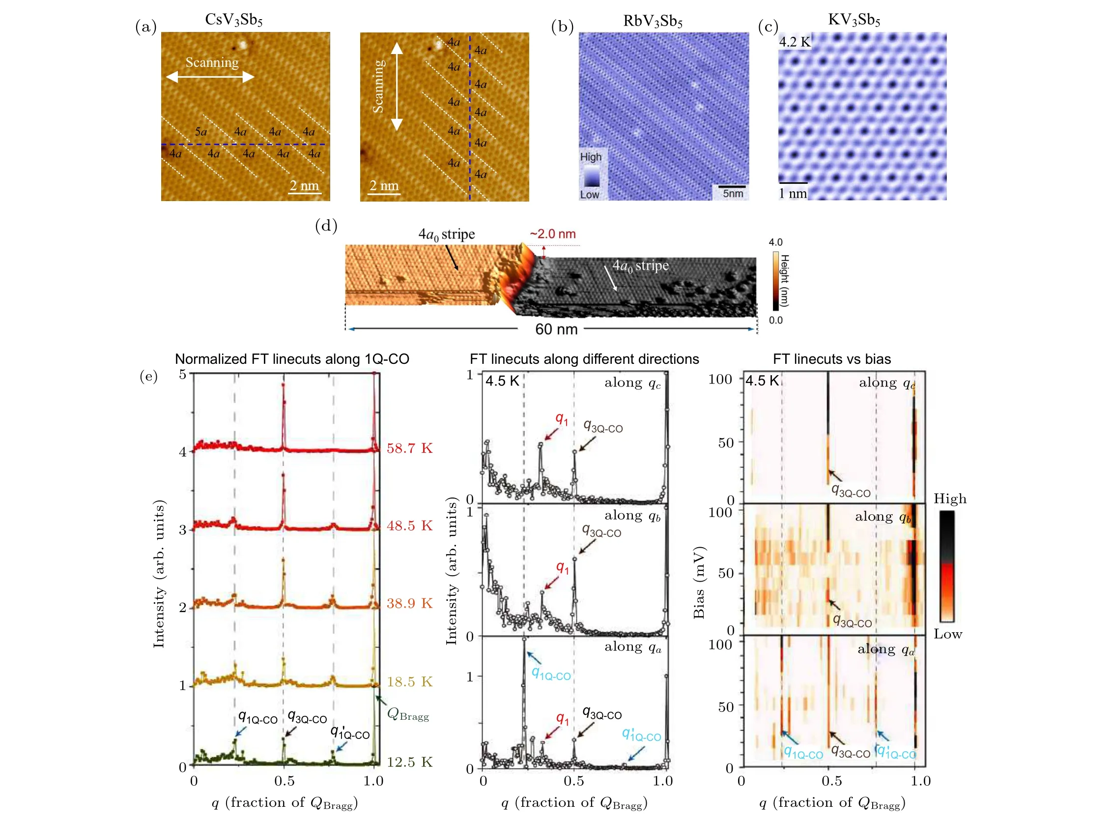
Fig.7. Stripe charge order in AV3Sb5. (a)-(c)STM images of CsV3Sb5(adapted from Ref.[19]),RbV3Sb5(adapted from Ref.[23]),and KV3Sb5(adapted from Ref. [39]), respectively. The positions of the stripes can be spatially shifted along the horizontal direction. Occasionally, the distance between two neighboring stripes changes from 4a0 to 5a0. (d)Observation of stripe order across the step edge(adapted from Ref.[72]). (e)The Fourier transform signal of stripe order at various temperatures,along different directions and at distinct scanning bias,showing that the non-dispersive and unidirectional stripe order disappears around 60 K(adapted from Ref.[45]).
To further understand the phenomenon of the TRSB of the 2×2 CDW, Fenget al.[67]introduced a chiral flux phase(CFP) in theAV3Sb5family. Based on a 2D model, and depending on the order parameter,a vector CDW,a charge bond order,and a charge CFP can be formed. The CFP has the lowest ground state energy compared with the other orders. Its relative charge configuration is shown in Fig. 8(c), in which two types of current flux loops form honeycomb lattice and hexagonal lattice are marked by red circle and blue circle,respectively. Combining these two distinct loops naturally gives rise to a 2×2 charge order. The Chern number is equal to 1 in the CFP by calculating the intrinsic Hall response, which can further support the results in Hall transport measurements,
where the non-quantized experimental Hall resistance may result from the complex multi-orbital effect. Furthermore, the same theoretical group[77]found as many as 183 flux phases on a kagome lattice within 2×2 unit cell after the proposed CFP and completed the classificational work by symmetry inspection. And a parallel theoretical work based on mean-field analysis was also proposed by Dinneret al.[68]
Yuet al.[22]claimed that the as-observed TRSB signal in zero-field muon spin relaxation experiment can be the evidence of chiral flux phase, but the transition temperature resides around 70 K,which does not fit the CDW transition temperature,may correspond to another hidden order.Meanwhile,Jianget al.[39]stressed that the chiral feature of 2×2 CDW can only occur at the surface defect-free region,but another STM group[70]denied the chirality and its filed tunability of CDW by using the low-temperature STM in KV3Sb5samples grown from the same group. Moreover,Liet al.[78]claimed that such chiral flux current in CsV3Sb5is not observed by utilizing the spin-polarized STM.Some optical experiments also provided strong evidence for detecting the TRSB. Xuet al.[79]performed scanning birefringence microscopy, magneto-optical Kerr effect and circular dichroism measurements and showed that inAV3Sb5system both a three-state nematicity and TRSB exhibit atTCDW. Bulk symmetry breaking state with twofold rotation symmetry in charge-density-wave was reported by Wuet al.using the optical polarization rotation method.[80]

Fig.8. Time reversal symmetry breaking charge order in AV3Sb5. (a)Spectroscopic 2×2 vector peaks taken at the impurity-pinning-free Sb surface region of KV3Sb5 by applying the magnetic field B=0 T,+2 T and-2 T,respectively,showing that the strength of intrinsic charge modulations exhibits chiral anisotropy with unusual magnetic field response(adapted from Ref.[39]). (b)The temperature dependence of the muon spin relaxation rate, showing the enhanced magnetic response of the charge order with applying external magnetic fields (adapted from Ref.[24]). (c) Theoretical prediction of chiral flux phase in the kagome superconductor AV3Sb5 (adapted from Ref.[67]).
The TRSB is alluring in the field of condensed matter physics,and the discovery of the TRSB[39]inAV3Sb5family has aroused enough research interests in the past two years.However,for a deeper understanding of the underlying mechanism, it still needs more experimental evidence, especially for the smoking-gun-like proof, and further theoretical proposal to connecting the diverse experimental results. Except for the theoretic works mentioned here, there are different proposals[68,69,81,82]postulated to try to uncover the underlying physics.
In this section, we have shown various experimental evidence of 2×2×2(4) CDW inAV3Sb5at first. Although the Fermi surface nesting and electron-phonon coupling can mainly account for its mechanism, different experimental results favor to support the electron-electron correlation scenario. The 2×2×2(4) CDW with momentum-depend energy gap was demonstrated by several ARPES groups, but the physics behind is still an open question. Besides, the rotation symmetry breaking states including the unidirectional 4a0charge order and electronic nematicity stimulate new research interest. Surprisingly, the discovery of TRSB bridges the 2×2×2(4)CDW to AHE and promotes the understanding the origin of the AHE.
4. Superconductivity in AV3Sb5
In addition to the anomalous charge orders, another intriguing property forAV3Sb5is the superconductivity. The research of superconductivity has triggered enough interests in many materials for a very long time,[83-88]especially for the unconventional superconductivity among the new materials in the past decades, such as cuprates,[89-91]iron-based superconductors,[92-94]and Ni-based superconductors.[95-97]Understanding the mechanism of superconductivity is of great significance in condensed matter physics. The kagome superconductorsAV3Sb5provide a new platform to understand and tune the superconductivity. Furthermore, the V-based superconductors may also contribute to the long sought-after topological superconductors,[98-101]which are the footstones for quantum computing.[102,103]
4.1. Basic characterizations of superconductivity
Despite the transport measurements have justified the superconductivity of all three kagome materials in theAV3Sb5family,[18,37,104]the microscopic evidence is still lacking. For the superconductivity,there are several key issues that are worthy to be addressed.
4.1.1. Strong coupling or weak coupling?
For CsV3Sb5, the spatially-averaged local densities of state on both Sb and Cs surface show V-shaped feature and finite zero-bias conductance[Fig.9(a)].The spectrum on the Sb layer exhibits a deeper zero-energy conductance and a sharper coherence shoulder than on the Cs layer at electron temperature of 300 mK.[19]The transition temperature of the superconductivity deduced from the temperature-dependent experiments is~2.3 K [Fig. 9(b)]. To further elucidate that the as-observed spectra are the superconductor density of state,a Josephson junction by using a superconducting tip is constructed [Fig. 9(c)]. The significant signals of the Josephson effect are shown in Fig.9(d).Additional,two thermal-induced symmetric in-gap peaks appear when temperature increases,and disappear at about~2.3 K, which is consistent with the normal tip case.[19]Based on the spatially-averaged superconducting gap size of~0.52 meV over the whole sample surface and transition temperature,the gap-to-Tcratio 2Δ/kBTcis~5.2,indicating a strong-coupled superconductivity from the perspective of local STM measurements.[19]On the other side,in the heat capacity measurements of KV3Sb5[Fig.9(e)],the fitted dimensionless specific jump at superconducting transition temperature (Tc) is estimated to be ΔCes/(γnTc)=1.03,which is quite small relative to the BCS weak coupling limit(ΔCes/(γnTc)=1.43). The inconsistence between the STM and heat capacity measurements suggests possible anisotropic gap function or multigap for theAV3Sb5.

Fig. 9. Observation of superconductivity in AV3Sb5. (a) Spatially-averaged dI/dV spectra obtained on the Cs and Sb surfaces of CsV3Sb5, showing a particle-hole symmetric V-shaped gap near EF and non-zero LDOS at zero-bias. (b) Color map of temperature dependent dI/dV spectra showing the disappearance of V-shaped gap at about 2.3 K.(c),(d)The observation of Josephson effect by using a superconducting tip,which provides strong evidence that the CsV3Sb5 is in the SC phase (adapted from Ref. [19]). (e) The specific heat capacity difference between the superconducting and normal states of KV3Sb5. The fitted dimensionless specific jump at Tc indicates a weak coupling superconductivity (adapted from Ref. [104]). (f) dI/dV spectra with ultra-high energy resolution,showing multiband superconductivity in CsV3Sb5 (adapted from Ref.[25]).
4.1.2. Single-gap or multigap?
The SC gap in dI/dVspectra of most low-temperature STS measurements shows a single SC gap near 0.5 meV.But it does not fit the single-gap Dynes function,implying the possible multi-band attribution of the superconducting state.[47]Meanwhile,Xuel al.reported two kinds of SC gaps with multiple set of coherent peaks and residual zero-energy density of states at both Cs and Sb surfaces [Fig. 9(f)], indicating that the superconductivity has band-dependent gap functions.[25]In addition, the temperature-depended curves of critical field in the transport measurements fit well with a two-gap model[Fig. 10(a)][105]and the temperature dependence of the inplane and out-of-plane components of the magnetic penetration depth[106]further support the multi-band nature of the superconductivity.
4.1.3. Isotropic or anisotropic?
Applying a magnetic field to CsV3Sb5, the zerotemperature out-of-plane and in-plane upper critical fields are determined to be 0.8 T and 7.2 T,respectively[Fig.10(a)].The coherence length for out-of-plane and in-plane can be deduced to be 2.2 nm and 20.3 nm, separately. And the lower critical fields along the two directions are both lower than 5 mT.Meanwhile, Niet al.[105]found that the angular-dependent magnetoresistance (AMR) shows a prominent two-fold symmetry under a magnetic field of 0.5 T in the mixed state,and the AMR slips 60°when the temperature changes from 2.8 K to 2.6 K. The origin of the observed AMR twist is not yet clear. Similar two-fold symmetry in the superconducting state was reported by Xianget al.[76][Fig.10(b)].
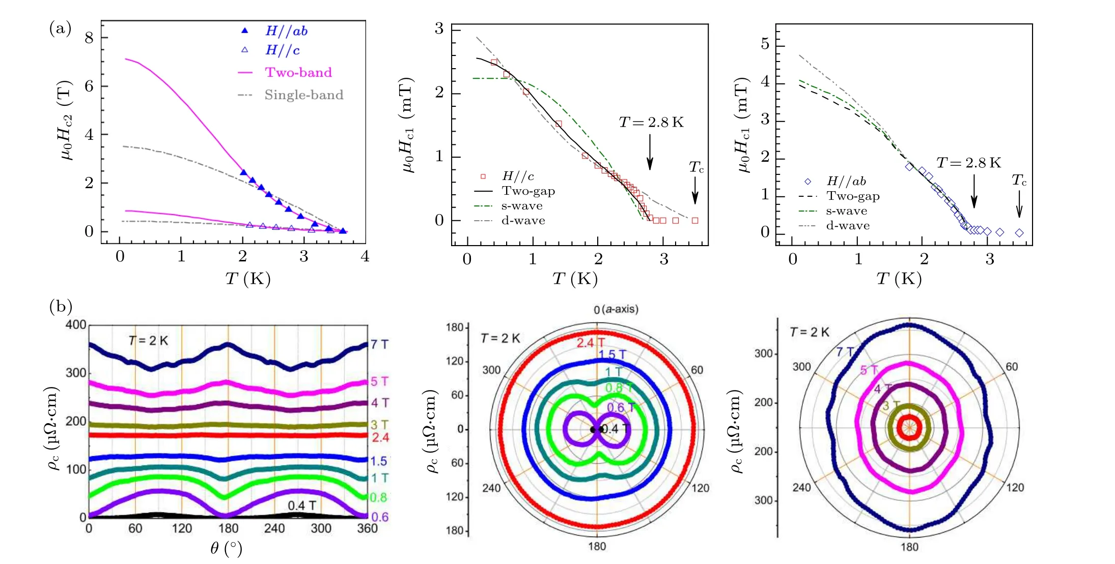
Fig. 10. Anisotropic superconducting properties of CsV3Sb5. (a) Temperature dependence of the upper critical fields and the lower critical field,showing that the upper critical field exhibits a large anisotropic ratio at zero temperature and fitting its temperature dependence requires a minimum two-band effective model(adapted from Ref.[105]). (b)The c-axis resistivity with the in-plane rotation of magnetic field showing a two-fold symmetry of superconductivity in the superconducting state and a unique in-plane nematic electronic state in normal state when rotating the in-plane magnetic field(adapted from Ref.[76]).
4.1.4. Nodal or nodaless?
The V-shaped feature and finite zero-bias conductance in the dI/dVspectra of CsV3Sb5[Fig.9(a)]cannot be obtained from the thermal broaden of a gapped superconductor spectrum at low temperature,indicating that the gapless states coexist with the superconductivity at zero temperature.[19]Besides, the muon spin relaxation/rotation measurement suggests that the superconductivity does not break the timereversal symmetry and shows unconventional nature.[106]In addition, the density-functional theory calculation shows that the electron-phonon coupling is too weak to account for such high superconductor transition temperature,implying the unconventionality of the superconductivity.[46]On the other hand,s-wave full gap superconductivity was uncovered by the121/123Sb NQR and51V NMR measurements.[107]The in-gap states in the dI/dVspectra could be induced by magnetic impurities but not by nonmagnetic impurities,suggesting a signpreserving or s-wave superconducting order parameter.[25]Based on the geometric structure of the kagome lattice,some theoretical models have been proposed to try to understand the mechanism of superconductivity and the observable low energy behavior,[26,108]a satisfactory model to reconcile all experimental results aboutAV3Sb5is still lacking.
4.2. Possible topological superconductor candidate
Another interesting property ofAV3Sb5kagome materials is the combination of superconducting ground state with intrinsicZ2topology,where the protected Dirac crossings are close to the Fermi level. The topological surface states are firstly proposed by the DFT calculations as well. Figure 11(a)shows the calculated band structure of CsV3Sb5,and displays theZ2topological invariant obtained by checking the parity of the wave function at the time-reversal invariant moment. Focusing on the surface state near the ¯Mpoint, there are Dirac crossings at the energy of about 0.05 eV above the Fermi energy, as shown in Fig. 11(b). Such surface states show anisotropic dispersions between ¯M-¯Γdirection and ¯M-Kdirection [Fig. 11(b)]. TheZ2topology is proposed for all three materials ofAV3Sb5family including the pristine, star of David and inverse star of David structures.[46]The topological surface states are evidenced by the ARPES measurement as shown in Figs.11(c)and 11(d).
The vortex bound states have been proved to be an ideal platform to study the topological nature of superconductors.The superconducting gap gradually induces with increasing the magnetic field perpendicular to the sample surface. When applying a magnetic field of tens of milli-Tesla perpendicular to the surface,the Abrikosov-vortices lattice is observed both at Cs surface and Sb surface.[19,25,47]However, the dI/dVlinecuts crossing the vortex core on the two surfaces show distinct behaviors. The bound states inside the vortex core collected at Sb surface exhibit a X-type evolution with spatial distance, while the ones at Cs surface exhibit Y-type evolution with a broad zero-bias peak at the core center[Figs.12(a)and 12(b)]. The X-type in-gap core states are usually thought to be trivial as it has been widely observed in conventional swave superconductors.[109-111]On the other hand, the Y-type features of in-gap core states may indicate the presence of Majorana bound states as reported in other superconductors with topological surface states.[112]

Fig.11. Topological band structures of CsV3Sb5. (a)Calculated band structure of CsV3Sb5 along high-symmetry directions across the Brillouin zone. A continuous direct gap(shaded)is noted and high-symmetry points in the Brillouin zone are labeled. (b)Tight-binding model of CsV3Sb5 showing topologically protected surface states that manifest at the time-reversal invariant momentum ¯M point (adapted from Ref. [18]). (c)-(d)Observation of topological surface state above the CDW transition temperature(c)and at 5 K(d)(adapted from Ref.[114]).
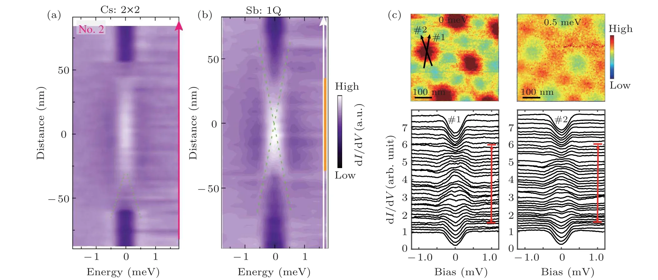
Fig.12.Vortex core-states in CsV3Sb5.(a),(b)Color map of the spatially resolved dI/dV spectra across the vortex at Cs and Sb surfaces,respectively,showing surface-dependent vortex-core states(adapted from Ref.[47]).(c)Vortex states measured on the Sb surface of CsV3Sb5 with ultra-high energy resolution,showing Caroli-de Gennes-Matricon states instead of zero-bias vortex bound states in the vortex core(adapted from Ref.[25]).
If the as-observed zero-bias peak is originated from Majorana bound states,how the Dirac surface states become superconducting as the calculated topological surface state is about 0.05 eV above the Fermi surface? One possibility is electronic reconstructions and doping effect induced by the alkali atom desorption.[113]Another possibility is the CDW state induced band shift evidenced by a recent ARPES work,[114]where the observed topological surface states are very close to the Fermi surface and further move down in the CDW state[Fig.11(c)].Comparing to the calculation,the lower energy of the topological surface states in the real materials activates the topological states for electron conduction in the superconducting state at low temperature [Fig. 11(d)]. To prove thatAV3Sb5family serve as an eligible candidate for the topological superconductor,ultralow temperature STM measurements and more experimental evidence are needed. It should be noticed that recent STM works with higher energy resolution claim that the broad peak in the near vortex core is asymmetric for the vortices at both Cs and Sb surfaces, which is consistence with Carolide Gennes-Matricon states instead of the zero-energy vortex bound states[Fig.12(c)].[25]
5. Competition between charge density wave and superconductivity
CDW and SC are similar in the perspective of mean field theory. They are both related to the electron-phonon coupling and Fermi surface instability, or affected by electronelectron interactions. In most cases, CDW is competing with SC,[115-117]and the situation inAV3Sb5family is no exception,especially under distinct pressure,chemical doping contents,thickness,and strains.
5.1. High pressure
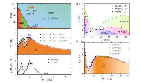
Fig.13. Phase diagram with pressure for AV3Sb5. (a)Phase diagram of CsV3Sb5 with pressure,showing the unusual competition of superconductivity and charge-density-wave(adapted from Ref.[118]). (b)Temperature-pressure phase diagram of AV3Sb5 (A=Cs, Rb and K),showing the universal double-dome superconductivity under pressure(adapted from Ref.[122]). (c)The high-pressure electrical measurements up to 150 GPa,showing a new superconducting phase to be rather robust(adapted from Ref.[123]).
TheAV3Sb5kagome superconductor shows an unusual competition of superconductivity and CDW.By applying pressure on the CsV3Sb5,the CDW is suppressing monotonically,which is accompanied by the increase of SC,showing the competition between CDW and SC.[20,118]It is rational to expect such competition since the released density of state from the suppressed CDW state will contribute to the enhancement of SC. By a closer inspection of the pressure-dependentTcof SC, two-dome feature is observed, where theTcshows two broad peaks at~0.7 GPa and 2.0 GPa with carrying a dip at~1.1 GPa [Fig. 13(a)].[118]The highest peak corresponding to 2.0 GPa is up to 8 K. Meanwhile, the upper critical magnetic field shows the same behavior asTc[Fig.13(a)],and the maximal value is as high as ten times larger than the initial one at ambient pressure.[118]The double superconducting dome is widely discovered inAV3Sb5family,[20,119-122], which manifests the non-trivial SC as well as the unconventional CDW[Fig.13(b)].[122]
The superconducting phase is also tuned by the high pressure due to the suppress of CDW. If the pressure increases further to 150 GPa, a new superconducting phase appears which is rather robust and inherently lined to the interlayer Sb2-Sb2 interactions[Fig.13(c)].[123]The formation of Sb2-Sb2 bounds at high pressure tunes the system from twodimensional to three-dimensional and pushes the pzorbital of Sb2 upward across the Fermi level,resulting in enhanced density of states and increase ofTc. In a recent pressure-tuned and ultra-low temperature muon spin spectroscopy,the superconducting state displays a nodal energy gap and a reduced superfluid density competing with a time-reversal-symmetry breaking charge order under low pressure. However, under high pressure,the charge-order transitions are suppressed,the superfluid density increases and the superconducting state progressively evolves from nodal to nodeless.[124]
5.2. Chemical doping
Another approach to study the competition between SC and CDW is the chemical doping. To avoid killing the superconductivity, doping elements should be carefully selected sinceAV3Sb5with much deficiency will not produce superconductivity.[17,18]The earliest attempt to bring superconductivity into the potassium-deficient and nonsuperconductive K1-xV3Sb5was done by Wanget al.,[125]
where they successfully fabricated a Josephson junction with K1-xV3Sb5, and introduced the spin-triplet Cooper pairs by the proximity effect. So far, two types of chemical doping through substation of partial elements have been achieved in experiments. One type is the chemical doping into the nonsuperconducting layer such as substation of Sn onto the Sb layer. The phase diagram for CsV3Sb5-xSnxshows a doping effect where the nearest van Hove singularity is shifted toward and aboveEF. The superconductivity exhibits a nonmonotonic evolution with doping content, resulting in two“domes” peaked at 3.6 K and 4.1 K and the rapid suppression of CDW [Fig. 14(a)].[126]The other type is the direct substitution of other 3d transition metal elements onto the V site in the kagome superconducting layer. The phase diagram for the CsV3-xTixSb5shows a doping effect as well. Ti doping induced two distinct phases have been discovered. The slightly-doped SC phase has a V-shaped SC gap, coexisting with CDW and AHE,indicating a strong-coupling unconventional SC nature. The highly-doped SC phase has a U-shaped SC gap where the CDW and AHE are undetectable.[127]TheTcin the Ti-doped sample has a little enhancement to about 3.5 K.For the Nb-doped system,theTcis enhanced monotonically to about 4.45 K.[128]
5.3. Thickness
The competition between CDW and SC is also observed in sample-thickness-depend experiments.[27]The evolution of CDW and SC with sample thickness in CsV3Sb5shows that theT∗decreases from 94 K in bulk to a minimum of 82 K at thickness of 60 nm,then increases to 120 K as the thickness is further reduced to 4.8 nm. TheTcshows an exactly opposite evolution, increasing from 3.64 K in the bulk to a maximum of 4.28 K at thickness of 60 nm, then decreasing to 0.76 K at 4.8 nm.[27]Songet al.also observed the competition of SC and CDW in selective oxidized CsV3Sb5thin flakes. The prominent effect of hole doping is achieved by the selective oxidation, which induces a superconducting dome as a function of the effective doping content. TheTcand upper critical field in thin flakes are significantly enhanced compared with the bulk ones[28][Fig.14(b)].

Fig. 14. Phase diagram with chemical doping, thickness, and strain for AV3Sb5 crystal. (a) Hole-doping phase diagram for CsV3Sb5-xSnx,showing the suppression of CDW and double-dome superconductivity with increasing doping contents (adapted from Ref. [126]). (b) Phase diagram of CsV3Sb5 with the variation of hole-doping content, where only the top layer is assumed to be oxidized, showing the competition of superconductivity and charge density wave in selective oxidized CsV3Sb5 thin flakes(adapted from Ref.[28]). (c)Point-contact spectroscopy at CsV3Sb5 and KV3Sb5,showing strain-sensitive superconductivity(adapted from Ref.[129]).
5.4. Strain
The stain-sensitive SC in KV3Sb5and CsV3Sb5has been observed in point-contact spectroscopy.Tcis enhanced in soft point contact spectroscopy and further enhanced in mechanical point-contact spectroscopy. The enhanced SC probably arises from local strain caused by the point contact, which leads to two-gap or single-gap behaviors observed in different point contacts[129][Fig.14(c)].
The competition between the CDW and SC provides the key clue for us to further increasing theTcof SC while suppressing the CDW.When theTcof SC goes beyond the helium-4 temperature range, the possible application may come out for the first generation. Meanwhile,AHE could be realized at a higher temperature if reducing the SC,since the CDW is intimately related to the AHE.Besides,the competition between CDW and SC provides a new platform for investigating the behavior of electrons in such a fertile system.
6. Pair density wave in CsV3Sb5
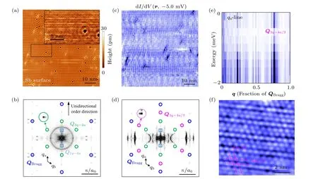
Fig.15.Observation of a new density wave at Q3q-4a/3 in CsV3Sb5.(a)-(d)The large-scale STM topography, dI/dV(r,-5 mV)map of Sb surface and corresponding Fourier transforms,showing the discovery of a new superlattice at Q3q-4a/3 highlighted by the magenta circles beyond 2×2 and 1×4 orders. (e)Energy dependence of the Fourier line cuts along one lattice direction as a function of energy,respectively,showing non-dispersive ordering vectors at Q3q-4a/3. (f)dI/dV(r,V)map near the pairing gap at 0.4 mV,after filtering out atomic Bragg peaks and incoherent background,exhibiting 4a/3 checkerboard modulation associated with the bidirectional PDW(adapted from Ref.[19]).
When Cooper-pairs spatially modulate with a wave vectorQ,the Cooper-pair density wave can occur. Historically,PDW was confirmed in only a few systems[130-133]due to the limitation of ultra-high spatial resolution technique and candidate of materials. Thanks to the ability of atomically-precise visualizing the density of state in both real and momentum spaces,spectroscopy-image STM becomes the a powerful tool in the progress of searching PDW.
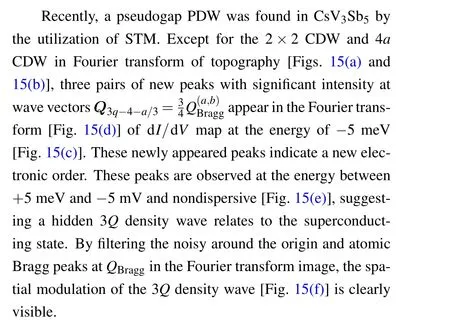
The observations of SC gap modulating at the same wave vectors demonstrate that the 3Qdensity wave is a PDW.In the one-dimensional case, the dI/dVlinecut along the 4astripe direction demonstrates that the SC gapΔ(r),zero-energy conductance(G0(r)= dI/dV(r,0)), and coherence peak height(P(r)= dI/dV(r,+Δ(r)))spatially modulate in a period of 4a/3 [Figs. 16(a)-16(d)]. To see the spatial modulation of the SC gap clearly, the second derivative is applied to the dI/dVgettingD(r,V)=-d3I/dV3(r,V), which has been also applied to study the PDW in the cuprate.[134]In the twodimensional case, the bidirectional property of the 3Q PDW on the hexagonal lattice is evidenced by the gap map and the corresponding Fourier transform(Fig.16(e)),similar to the results in cuprates[131]and NbSe2.[133]
Fig. 16. Spectroscopic evidence of PDW at Q3q-4a/3 in CsV3Sb5. (a) Evolution of the differential conductance dI/dV(r,V) and negative of its second derivative D(r,V)=-d3I/dV3(r,V) along a linecut in qb-direction, respectively. (b) Plot of 2Δ(r) and the corresponding Fourier spectrum,showing the 4a/3 spatial modulation highlighted by the pink dashed line marked by Q3q-4a/3. (c)Spatial modulations of coherence peak height P(r), SC gap depth H(r), and zero-bias conductance G(r). The spectra are offset for clarity. (d)Beating pattern simulated using Q3q-2a(green curve)and Q3q-4a/3 (pink curve), showing consistency with Bragg-filtered modulations of P(r)and H(r). (e)Superconducting gap map Δ(r). (e)Fourier transform of superconducting gap map Δ(r),showing clearly Q3q-4a/3 modulations of gap size. (f)Schematic illustration of the roton-PDW(adapted from Ref.[19]).
To gain further understanding of the observed PDW,correlation between the modulation of zero-energy conductanceG0(r) and coherence peak heightP(r) is studied. The modulations ofP(r) andG0(r) are out of phase, while the modulations ofP(r) and the gap-depth (H(r)=P(r)-G0(r))are in phase[Fig.16(c)]. Because coherence peak heightP(r)has the positive correlation with the superfluid density[135]andG0(r)is associated with the normal fluid density,the relations betweenP(r),H(r)andG0(r)present an unprecedented electronic density wave modulation of superconductivity. Therefore, the as-observed PDW exhibits similar behaviors with the shallow roton minimum, where they are spatially modulated at the same vectorQpdw=Qroton=Q3q-4a/3. The superfluid density and normal fluid density naturally emerge as anti-correlated on the vortex-antivortex lattice,accounting for the spatial modulation of zero-bias conductance and coherence peak height. The commensurate hexagonal vortex-antivortex lattice,which is from the zeros of the complex order parameter of PDW,forms the roton-PDW[Fig.16(f)].

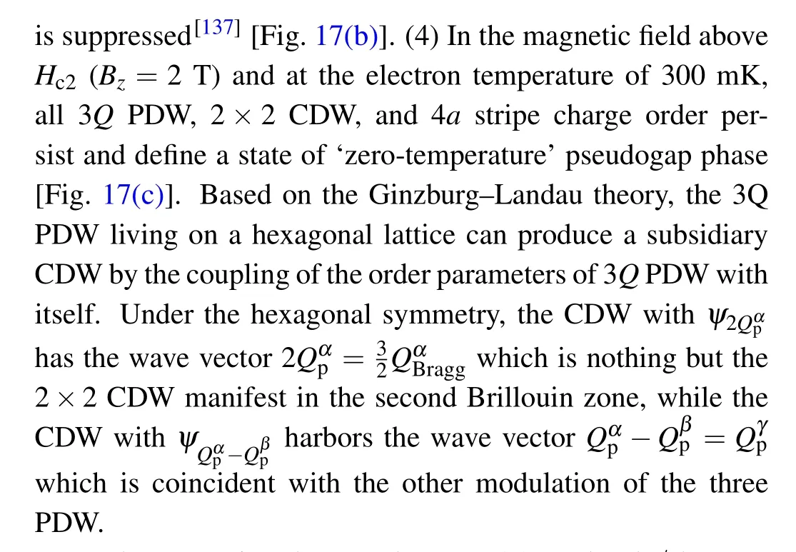
When warming the sample up to 4.2 K, the dI/dVmap remains all the charge order as observed in the superconducting state, implying that the PDW state can coexist with other intertwined charge orders in the normal state[Fig.17(d)]. The peak around~±5 meV manifesting as the magnitude of the pseudogap becomes sharper when the system going into a superconducting state,especially in the condition of the 0 T magnetic field [Fig. 17(a)]). Despite that the PDW itself is not coherent, the order parameter of PDW can couple to the SC condensate ΔSCto transform the incoherent peak into coherent when stepping into SC state. It is the best explanation to correspond such a peak to the PDW since a CDW should almost preserve its peak shape both in the normal state and the superconducting state. Besides, the pseudogap size itself also exhibits spatial modulations at the 3Q Q3q-4a/3wave vector[Fig.17(e)],further demonstrating the 3QPDW associated with the pseudogap as a mother state.
Recently,quantum oscillations with periodicities ofh/4eandh/6eare discovered in CsV3Sb5, providing direct evidence for the existence of charge-4eand charge-6esuperconducting condensate.[138]Charge-2e, charge-4eand charge-6esuperconducting condensate exist in different temperature regions, below 1.0 K for charge-2e, 1.0~2.3 K for charge-4eand 2.3 K~Tcfor charge-6e,respectively. The charge-4eand charge-6esuperconducting are possible vestigial electronic ordered states. The charge-2eroton PDW state is revealed at~0.3 K.It is proposed that deep in the PDW state,both translation and rotation symmetry are broken. As the temperature increases, the rotation symmetry and translation symmetry restore in sequence,leading to existence of charge-4eand charge-6esuperconductivity,respectively.
The roton-PDW is discovered in CsV3Sb5, which satisfies the definition of PDW and behaves like a roton with anti-correlation to the superfluid density. Such a novel PDW is distinct from the trivial one which can be deduced from the CDW in the superconducting state, serving as a “mother state” corresponding to the pseudogap and can generate subsidiary CDW in charge sector which can be detected by STM in our case. This PDW also survives in the normal state and“zero-temperature” phase where the superconductivity is removed, manifesting itself as a density wave of the preformed Cooper pair, making theAV3Sb5family a promising platform to further study the mechanism of pair density wave superconductivity.[139,140]
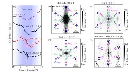
Fig. 17. Spectroscopic evidence of ‘mother state’ PDW corresponding to the pseudogap. (a) Spatially-averaged dI/dV spectra obtained under different physical conditions of magnetic field and temperature,showing the spectral changes and the presence of the low energy pseudogap. (b)-(d) The magnitude of drift-corrected, two-fold symmetrized Fourier transform dI/dV(r,-5 mV) map at 300 mK, 0.04 T (b), 300 mK, 2.0 T (c)and 4.2 K,0.0 T(d),respectively,showing the appearance of the density wave at Q3q-4a/3 under distinct conditions. (e)Fourier transform of the pseudogap map showing peaks at the PDW vectors Q3q-4a/3 circled in magenta(adapted from Ref.[19]).
7. Summary and outlook
Fig.18. Summary of the emergence of exotic physical phenomenon in CsV3Sb5 at distinct temperature ranges(the temperature ranges are taken from the references as labeled).
In this review, we summarize the recent progress on theAV3Sb5kagome materials. We focus on the main properties ofAV3Sb5in four aspects: (1) Giant AHE is demonstrated inAV3Sb5, showing the biggest Hall conductivity in kagome materials, but its origin is still unknown. (2) CDW shows unconventional behaviors, where the 2×2 CDW exhibiting time-reversal symmetry breaking may be associated with the giant AHE and the mechanism needs further exploration, the 4astripe charge order(under the debate whether coming from bulk or surface) is nontrivial as well. (3) Unconventional strong coupling superconductivity encounter withZ2topology can provide possible Majorana zero mode despite the superconductor gap function is still unclear,and the competition between CDW and SC provides more details to uncover the hidden physics. (4) Intrinsic PDW brings non-trivial properties,such as a roton-like behavior manifesting the anti-correlation between superfluid density and normal fluid density, serving as a “mother state” corresponding to the pseudogap which can produce CDW in the same wave vector. The discovery ofAV3Sb5kagome materials not only enriches the research of exploring the next-generation quantum device but also appeals plenty of fundamental research interests,providing a fertile platform to study the interplay among AHE,topology,flat band,CDW,SC,and PDW.All the above physics phenomena emerge at distinct temperature ranges in CsV3Sb5,one representative material inAV3Sb5family,are plotted as a summary graph in Fig.18.
Despite many experimental results that have been included in the review, some works are still in progress and an abundance of unconventional properties are to be explored in this field.
First, the origin of CDW should be further determined,including both 2×2×2(4)and 4aCDW.The relations among time-reversal symmetry breaking, 2×2 CDW, and AHE are waiting to be uncovered both on the experimental side and theoretical side. Although some theoretics propose diverse models[26,46,67-69,77]to try to understand all the physics related to the CDWs, a complete solution to reconcile all experimental results and predicting new phenomena is still lacking.Besides,contradicting experimental results[39,70,78]on the determination of the chiral CDW should be explained in a consistent way. A similar debate[19,45,75]on the origin of the 4astripe charge order is also calling for more works in the future.Very recently, CDW has been discovered within an antiferromagnetic ordered phase of kagome lattice FeGe by neutron scattering[141]and STM.[142]The CDWs are found to share many features withAV3Sb5but show distinct features such as strong correlation driven band renormalizations, appearance of edge states and enhancement of the magnetic moments below the CDW transition temperature.[143]The newly discovered CDWs in FeGe indicate the universal origin of charge orders in both superconducting and magnetic kagome materials.
Second,the SC gap function and the band structure below SCTcrequire more studies. So far, it is difficult to study the band structure at the superconducting state as most APRES instruments work at a temperature higher thanTc~2.5 K.One of the solutions is to increase the SC transition temperature, such as applying pressure and reduce the sample thickness as introduced in Section 5. Moreover, the layered structure inAV3Sb5with Van de Waals interlayer coupling provides further opportunities to obtain one-unit cell twodimensional kagome materials by exfoliation for deeper exploration of these and other unexpected challenges in the lowenergy many-body physics.
Third, more investigations related to PDW, such as theπphase winding in the PDW order near the CDW dislocation and the Josephson tunneling process related to the Cooper pair detection, should be put on the agenda. The real roton mode related to the bosonic excitation is elusive. Such a mode can be detected in the tunneling process through the electronmode coupling,as many kinds of bosonic modes were verified by different STM groups[144-147]in the past. Furthermore,the band structure of PDW needs more investigations as well.
Finally, the discovery ofAV3Sb5inspires exploration of more quantum materials based on kagome lattices. New families of V-based kagome compounds such asReV6Sn6(Re=Gd, Ho),[148]V3Sb2,[149]V6Sb4,[150]AV6Sb6[151]andAV8Sb12[152,153]have recently been proposed and partially synthesized. In addition, a series of candidate kagome superconductors based onAV3Sb5crystal structure are also predicted.[154,155]Except for the 135 system, new flat band materials hosting kagome sublattices[156]have been recently predicted.
In general, the study of kagome materials itself is a promising research field with plenty of exotic properties.When the kagome structure meets with multiple electronic orders,a plethora of new phenomena emerge and appeal a diversity of researchers joining from different research fields. We expect new discoveries for new physics and applications based on this family of materials.
Acknowledgments
We are grateful to Profs. Ziqiang Wang, Sen Zhou, Xiaoli Dong,Fang Zhou,Li Yu,Yan Zhang,Lin Zhao,Xinjiang Zhou, Rui Zhou, Qingming Zhang, Binghai Yan, Kun Jiang,Jiangping Hu for helpful discussions and suggestion. We acknowledge the financial support from the Ministry of Science and Technology of China,the National Natural Science Foundation of China and Chinese Academy of Sciences.
猜你喜欢
恋爱婚姻家庭(2022年22期)2022-09-08
国画家(2022年3期)2022-06-16
——评陈辉《浙东锣鼓:礼俗仪式的音声表达》
美育学刊(2022年2期)2022-04-11
保健与生活(2022年8期)2022-04-08
民间文学(2019年12期)2019-05-26
男生女生(银版)(2016年5期)2017-01-17
男生女生(银版)(2016年5期)2017-01-17
幼儿时代·故事妈妈(2004年3期)2004-03-17
- Chinese Physics B的其它文章
- Characterizing entanglement in non-Hermitian chaotic systems via out-of-time ordered correlators
- Steering quantum nonlocalities of quantum dot system suffering from decoherence
- Probabilistic quantum teleportation of shared quantum secret
- Spin–orbit coupling adjusting topological superfluid of mass-imbalanced Fermi gas
- Improvement of a continuous-variable measurement-device-independent quantum key distribution system via quantum scissors
- An overview of quantum error mitigation formulas