
Enhanced photon emission by field emission resonances and local surface plasmon in tunneling junction
2022-11-21 09:29JianMeiLi李健梅DongHao郝东LiHuanSun孙丽欢XiangQianTang唐向前YangAn安旸XinYanShan单欣岩andXingHuaLu陆兴华
Chinese Physics B 2022年11期
关键词:兴华
Jian-Mei Li(李健梅) Dong Hao(郝东) Li-Huan Sun(孙丽欢) Xiang-Qian Tang(唐向前)Yang An(安旸) Xin-Yan Shan(单欣岩) and Xing-Hua Lu(陆兴华)
1Beijing National Laboratory for Condensed Matter Physics,Institute of Physics,Chinese Academy of Sciences,Beijing 100190,China
2Key Laboratory for Microstructural Material Physics of Hebei Province,School of Science,Yanshan University,Qinhuangdao 066004,China
3School of Physical Sciences,University of Chinese Academy of Sciences,Beijing 100190,China
4Center for Excellence in Topological Quantum Computation,Beijing 100190,China
5Songshan Lake Laboratory for Materials Laboratory,Dongguan 523808,China
We investigated the photon emission spectra on Ag(111)surface excited by tunneling electrons using a low temperature scanning tunneling microscope in ultrahigh vacuum. Characteristic plasmon modes were illustrated as a function of the bias voltage. The one electron excitation process was revealed by the linear relationship between the luminescence intensity and the tunneling current. Luminescence enhancement is observed in the tunneling regime for the relatively high bias voltages, as well as at the field emission resonance with bias voltage increased up to 9 V. Presence of a silver (Ag)nanoparticle in the tunneling junction results in an abnormally strong photon emission at the high field emission resonances,which is explained by the further enhancement due to coupling between the localized surface plasmon and the vacuum. The results are of potential value for applications where ultimate enhancement of photon emission is desired.
Keywords: scanning tunneling microscopy,luminescence,surface plasmon,field emission resonance
1. Introduction
Electro-optical phenomenon on a nano-meter scale is important for designing micro and nano photonic devices,as well as for understanding the basic physical principles in light–matter interactions.[1–3]For example, light emission from atomic chains reveals electronic transitions between the discrete energy levels rooting from quantum confinement.[4–6]As another example, the local photon emission from a single molecule in the tunnel junction is caused by inelastic scattering of the tunneling electrons.[7–9]The photo luminescence can also be observed on semiconductor surfaces due to tipinduced carrier recombination.[10,11]The light intensities in these systems are affected by several factors, including electronic current, sample bias, local environment, and quantum efficiency (QE) of electron–photon conversion. For a typical gap antenna nanostructure,the value of QE is on the order of 10-4,[12–14]but it can be increased to 10-2when high concentration of hot carriers is induced by laser illumination in the tunneling gap.[15,16]The local environment,or even an atomic perturbation, may play an important role in determining the emission spectrum. Examples include a single defect in semiconductor,an extra atom attached to quantum dot,or a chemical group bonded to the functioning molecule. Detailed investigation in these delicate effects is strongly desired in order to fully understand the underlying mechanism and to explore into new applications.
Scanning tunneling microscope(STM) has been playing a unique role in studying light–matter interactions on a microscopic scale. It provides topographic details with atomic spatial resolution,and it can be employed to create vertical metalinsulator–metal structures (MIMs) as a gap antenna,[17,18]
where the inelastic tunneling electrons excite localized surface plasmons(LSP).In the STM configuration,the tunneling gap can be adjusted by changing the sample bias voltage, while keeping the tunneling current at a constant level. When the bias voltage is set to be higher than the work function of the metal, the system turns into the field emission regime where the intensity of light emission exhibits oscillation as a function of the bias. The luminescence reaches its local maximum value at some specific bias voltages, which is known as the field emission resonance(FER)associated with the hot electron injection and the inelastic electrons tunneling (IET)through the field emission state.[19,20]While several seminar studies have demonstrated the advantages of the STM-based investigations,the influence of local environment on the electron photo luminescence as well as the coupling to the FER has not been fully explored on a nanometer scale yet.
Here, we examine the photo luminescence from the tunneling junction with an Ag STM tip on Ag(111)surface. The light emission intensity as a function of the sample bias and the tunneling current is examined. Special attention is paid to a local perturbation with an Ag nanostructure deposited on the surface, where an abnormal enhancement in the emission spectra is observed.The correlation between the luminescence intensity and the field emission resonance is investigated and explained by the plasmon resonance in the nano-cavity and the electronic local density of states.
2. Experiment
The experiment was performed by using a homebuilt STM in ultrahigh vacuum with a base pressure of 1×10⁻¹⁰Torr(1 Torr=1.33322×10²Pa). The Ag(111)surface was cleaned by cycles of argon ion sputtering and annealed at 600°C.The Ag tips were prepared by electrochemical etching from 99.99%Ag wires(Nilaco Corporation)with a diameter of 500 μm.The tips were further cleaned by filament heating, ion sputtering, and finally treated by voltage pulses on clean surfaces. Photons emitted from the tunnel junction were collected by two convex lens(f1=50 mm,Φ1=15 mm,f2=15 mm,Φ2=15 mm) and focused into an optical fiber outside the vacuum chamber which guided the light to a spectrometer (Spectra Pro 2300, Princeton Instruments) for analysis as shown in Fig. 1(a). Spectra in a wavelength range from 400 nm to 980 nm were acquired by a liquid-nitrogencooled charge-coupled device(CCD)with an integration time of 60 s. During acquisition,the STM tip was positioned statically above the sample with feedback loop on.
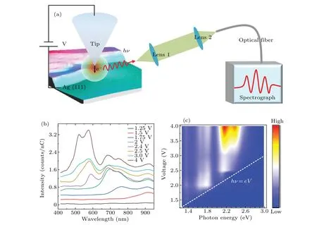
Fig.1. (a)Schematic diagram of STM-based luminescence experiment. (b)Luminescence spectra on Ag(111)surface with Ag tip under various bias voltages,with the spectra shifted vertically for clarity. (c)Spectrum intensity map corresponding to panel(b),displaying the relationship between the photon energy and sample bias,with dashed line indicating the boundary hν =eV.
3. Results and discussion
Figure 1(b) shows the characteristic luminescence spectra acquired on an atomic flat Ag (111) surface, under various bias voltages from 1.5 V to 4 V.For the low bias voltageV=1.5 V, there is only one peak present in the spectrum at the wavelength of 920 nm (hν=1.35 eV). For the high bias voltageV=4.0 V,multiple peaks can be identified in the spectrum. These luminescence peaks originate from the decay of plasmon modes that are excited by the electrons through inelastic tunneling process.[5,17,21]Figure 1(c) shows the spectrum intensity map as a function of photon energy and the bias voltage. The dashed line indicates a boundary where the maximum electron energy equals the photon energy. It is clear that all spectra obey the relationhν <eV,i.e.the photon energy is limited by the bias voltage, illustrating the quantum cutoff in single electron excitation process.[21]It is worth noting that the luminescence peak at 518 nm (photon energy 2.4 eV) is not obvious in the spectrum obtained under the bias voltage of 2.4 V.In addition,the intensities of two high energy peaks(respectively at wavelengths of 575 nm and 518 nm)rise quickly with the bias voltage increasing. The overall features in the spectra map can serve as a fingerprint of the plasmon modes in the nano-resonator constructed by the crystal surface and the specific STM tip apex.[12]
The intensity of luminescence spectrum depends on the magnitude of the tunneling current. Figure 2(a) shows three spectrum peaks measured as a function of the tunneling current, performed with a different Ag tip. The bias voltage is set to be±4.5 V, and the tunneling current is set to be between 2 nA and 8 nA (negative current corresponds to negative bias voltage). The integration time is 60 s for each spectrum. The energy values of three spectrum peaks are 1.66 eV, 1.80 eV, and 1.94 eV, respectively. There is no obvious change of the peak position or the peak width(FWHM)of each mode,implying that the cavity resonance remains unchanged over the investigated range of current intensities or gap distances,which is in agreement with the results reported previously.[22]The current-dependent luminescence peak intensity(maximum)is further fitted by the power lawIβ. The exponential constant turns out to beβ ≈1.0±0.05 for all three modes,which is in consistence with the single electron excitation process.[21,23]

Fig.2.(a)Luminescence spectra from Ag tunneling junction acquired under various tip-sample distances. (b) Plots of intensity versus current for three spectrum peaks.
We then investigate the luminescence spectrum by extending the bias voltage from 3 V to 9 V. The intensities of luminescence peaks on Ag surface reach a maximum value at the bias voltage of about 4.0 V, and decrease as the bias voltage increases further as shown in Fig.3(c). The observation of maximum in luminescence intensity as a function of the bias voltage is consistent with previous results,[20,24–26]and can be explained below. The electronic band structure of Ag (111) has a band edge position about 4 eV above the Fermi level(work function of Ag is about 4.6 eV.[27–29]). As bias voltage increases,the number of decay channels involving the photon emission increases. On the other hand, when the bias voltage increases from the tunneling regime to the field emission regime,the gap distance increases faster and deviates from a logarithmic fashion. The increased gap distance weakens the tip-sample electromagnetic coupling and subsequently quenches the photon emission. Typically, the peak intensity decreases by a factor of ten when the bias voltage increases from 4 V to about 9 V.
The profile of the luminescence is strongly dependent on the tip shape. We intentionally modify the tip by applying a voltage pulse to the sample as shown in Fig. 3(a). The topograph of the surface after the tip modification is shown in Fig. 3(b), where an Ag nanoparticle about 10 nm in size is deposited near the edge of a flat terrace. The luminescence spectrum is measured again by using the new tip(named tip 2)on the flat region of the surface(as marked in Fig.3(b)). The spectra, as shown in Fig. 3(c), display a two-peak feature as compared with the three-peak feature in the spectra acquired by the original tip(tip 1). The luminescence peaks as acquired by tip 2 are located at slightly lower energy, which indicates the presence of a sharper STM tip.[12]The peak intensity decreases significantly as the bias voltage increases up to 9 V,the trend of which is consistent with that of the results obtained by tip 1. Figure 3(d)shows the bias voltage-dependent luminescence spectra taken on the Ag nanoparticle created by tip modification.The tunneling current is kept at 2 nA.The profile of the spectra is very similar to that taken on the terrace,with two peaks at the same photon energy values of 1.63 eV and 1.82 eV. The intensities of both peaks, however, show strong variations as the bias voltage increases to the field emission regime as indicated in Fig. 3(e). The intensities of the two peaks have a few local maximum values with respect to the bias voltage. The first maximum value is seen at the bias voltage of 4.5 V,and the other three maximum values occur at the bias voltages of 6.2 V,7.5 V,and 8.5 V,respectively.As is well known,those maximum values at the bias voltages more than 5 V are related to the field emission resonance. The photon energy under such a resonance condition is determined by the relationshiphν=eVbias-En, (n=1, 2 ,3, ....), whereEnis the energy of the field emission resonance state in the system.The average of two emission modes is used in above relationship analysis andEnis determined to be 4.5 eV, 5.8 eV, and 6.8 eV,forn=1,2,3,respectively,marked by blue rectangles in Fig.3(f).

Fig. 3. (a)–(b) STM images of clean Ag (111) surface and Ag nanoparticle deposited on the surface, with image size being 180 nm×180 nm, and imaging condition V =3 V and I =0.3 nA. Luminescence spectra are obtained at different locations on the surface as marked by the arrows, with a constant tunneling current of 2 nA.The inset shows the line profile of Ag nanoparticle. (c)Luminescence spectra obtained with two different Ag tips on the flat region of Ag(111)surface under various bias voltages. The spectra are shifted vertically for clarity. (d)Luminescence spectra measured with Ag tip 2 above the Ag nanoparticle as shown in panel(b). The bias voltage is set to range from 3.5 V to 9 V,and the constant tunneling current is set to 2 nA,with NP denoting nanoparticle. (e)Luminescence peak intensity as a function of the bias voltage,with photon energy values of the two modes being 1.63 eV(red)and 1.82 eV(black). (f)The experimental differential conductance measured at constant current(2 nA)with tip 1 on Ag(111),with blue rectangles marking energy values of the first three FERs.
It is interesting to note that the peak intensities at different levels of the field emission resonances do not change monotonically. Instead, significant increase in peak intensity is observed at the resonance leveln=3, which is very different from the normal situation where the peak intensity decreases monotonically for higher level of the field emission resonance.[20]This enhancement at higher field emission resonance can be seen obviously due to the presence of the Ag nanoparticle. The schematic diagram for this enhancement mechanism is shown in Fig. 4. We calculate the electronic enhancement by the finite element analysis method. The incident laser illuminates the tunneling gap at an angle of 45°.The photons originate from the radiation attenuation of the local surface plasmons between tip and sample,and are assisted by the inelastic tunneling electrons from the Fermi level of the tip into the field emission resonance states. The energy values of the emitted photon are the same for the tip parked over the plat terrace and above the nanoparticle.This is reasonable since the energy of the plasmon mode is mainly determined by the radius of the curvature of the tip and the tip-sample distance. On the plat terrace,the efficiency of the photon emission is mainly determined by the tip profile where the contribution from the surface is much weaker due to the mismatch in their wave vectors between the propagating surface plasmon mode and the free photon in vacuum. As shown in Fig. 4(b), the presence of nanoparticle results in significant increase in electric field emission. The increased emission is due to the breaking of the translational symmetry of the plan surface,which permits surface plasmon along the sample-vacuum interface to decay radiatively.[30]In other words,the interaction between the localized surface plasmon of the nanoparticle on the surface and the emitted photon results in an extra enhancement effect.[31]
We estimate the quantum efficiency of the photon emission excited by the tunneling electron in such a nano-resonator,which can be expressed as
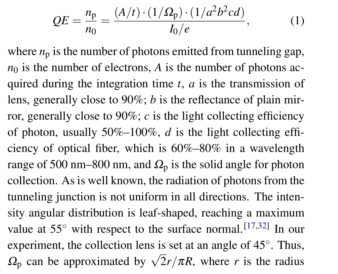


Fig.4. (a)Schematic representation of surface plasmons and electron luminescence in STM tunneling junction, with ω representing the frequency of plasmon mode within the tip-surface resonant cavity,excited by the inelastic scattering of tunneling electrons or field emission electrons. (b)Gap modes of the coupled systems with a stronger field enhancement than the plasmon modes of tip and substrate.(c)Nanostructure of tip and Ag substrate(diameter 40 nm,gap 1 nm)with a maximum enhancement factor of 432 at 1.90 eV.(d)Nanostructure of tip and Ag nanoparticle(diameter 10 nm,height 4 nm)on substrate with a maximum enhancement factor of 885 at 1.90 eV.
4. Conclusions
In this work, we investigated the electron luminescence spectra in the tunneling junction of an ultrahigh vacuum lowtemperature STM. The well-defined luminescence peaks are observed to be related to the plasmon modes of the tip-surface cavity. The light intensity is linear with respect to the tunneling current, indicating an electron excitation process. Enhanced luminescence enhancement is observed by the field emission resonance for high bias voltages in the tunneling regime. Abnormal enhancement in photon emission for the higher level of field emission resonance reveals the distinct role of the Ag nanoparticles on surface.The research results in this case provide a detailed understanding of light–plasmon interaction that are essential for many applications such as light harvesting and nano-antenna.Acknowledgements
Project supported by the National Natural Science Foundation of China (Grant Nos. 21961142021, 11774395, and 11727902),the Strategic Priority Research Program(B)of the Chinese Academy of Sciences (Grant No. XDB30201000),and the Beijing Natural Science Foundation, China (Grant No.4181003).
猜你喜欢
农业工程学报(2022年8期)2022-08-08
美与时代·美术学刊(2022年3期)2022-04-27
小学生必读(低年级版)(2021年9期)2021-12-29
小学生必读(低年级版)(2021年10期)2021-12-02
华人时刊(2021年17期)2021-11-12
音乐天地(音乐创作版)(2021年11期)2021-02-18
奇闻怪事(2020年9期)2020-11-20
老友(2019年9期)2019-10-23
金沙江文艺(2019年7期)2019-07-29
金沙江文艺(2017年4期)2017-03-31

- Chinese Physics B的其它文章
- A design of resonant cavity with an improved coupling-adjusting mechanism for the W-band EPR spectrometer
- Photoreflectance system based on vacuum ultraviolet laser at 177.3 nm
- Topological photonic states in gyromagnetic photonic crystals:Physics,properties,and applications
- Structure of continuous matrix product operator for transverse field Ising model: An analytic and numerical study
- Riemann–Hilbert approach and N double-pole solutions for a nonlinear Schr¨odinger-type equation
- Diffusion dynamics in branched spherical structure