
From microelectronics to spintronics and magnonics
2022-11-21 09:34XiuFengHan韩秀峰CaiHuaWan万蔡华HaoWu吴昊ChenYangGuo郭晨阳PingTang唐萍ZhengRenYan严政人YaoWenXing邢耀文WenQingHe何文卿andGuoQiangYu于国强
Chinese Physics B 2022年11期
Xiu-Feng Han(韩秀峰), Cai-Hua Wan(万蔡华), Hao Wu(吴昊), Chen-Yang Guo(郭晨阳), Ping Tang(唐萍),Zheng-Ren Yan(严政人), Yao-Wen Xing(邢耀文), Wen-Qing He(何文卿), and Guo-Qiang Yu(于国强)
Beijing National Laboratory for Condensed Matter Physics,Institute of Physics,Chinese Academy of Sciences,University of Chinese Academy of Sciences,Beijing 100190,China
In this review, the recent developments in microelectronics, spintronics, and magnonics have been summarized and compared. Firstly,the history of the spintronics has been briefly reviewed. Moreover,the recent development of magnonics such as magnon-mediated current drag effect(MCDE),magnon valve effect(MVE),magnon junction effect(MJE),magnon blocking effect(MBE),magnon-mediated nonlocal spin Hall magnetoresistance(MNSMR),magnon-transfer torque(MTT)effect, and magnon resonant tunneling (MRT) effect, magnon skin effect (MSE), etc., existing in magnon junctions or magnon heterojunctions, have been summarized and their potential applications in memory and logic devices, etc., are prospected,from which we can see a promising future for spintronics and magnonics beyond micro-electronics.
Keywords: magnon valve effect,magnon junction effect,magnon resonant tunneling effect,magnon-transfer torque effect
1. Introduction
Nowadays our daily life including working, communication, and entertainment has been greatly facilitated by the advanced information technologies, such as mobile internet,internet of things, 5G communications, artificial intelligence,clouds computing, and big data, all of which have been built on the basis of sophisticated microelectronics and are still benefiting from the emerging technologies such as high-κdielectrics,[1]FinFET,[2]and Gate-All-Around.[3]Even so,the conventional CMOS-based microelectronics are struggling in the competition between knowledge explosion and performance updating of microelectronics. As a sign of this rivalry,the Moore’s law which succeeds in guiding downscaling and upgrading of microelectronics for the last half century is expected to doom in the near future.[4]Thus, present is also a big chance for new paradigms to upgrade microelectronics.In the following and Fig. 1 we will retrospect the history of microelectronics, spintronics, and magnonics briefly, which hopefully helps us to envision some emerging research field or directions for the subsequent development of spintronics and magnonics beyond micro-electronics.
2. Main progress
As one promising alternative to the classic microelectronics,spintronics which introduces electron spin into electronics has been devoted long-focused efforts and expectations. As a milestone of spintronics, the discoverers of the giant magnetoresistance (GMR) effect,[5,6]Albert Fert and Peter Gruenberg were awarded the Nobel physics prize in 2007. Their discovery of the GMR effect and the subsequent spin valve devices have brought about a revolution for storage industry from Mega bit to Tera bit per inch square.[7]
In the subsequent development of spintronics,another device, the magnetic tunnel junction (MTJ),[8–12]functions as the key element, analogue to the field-effect transistor (FET)for the conventional microelectronics.An MTJ is mainly composed by a tunnel barrier(as a~1 nm amorphous Al–O barrier layer)and two adjacent magnetic layers(as CoFe or CoFeB alloys electrodes)whose magnetization directions are reversible for the free layer or fixed for the reference layer. Resistance of an MTJ depends on its magnetic states, low(high)resistance for the parallel(antiparallel)states normally,which is then encoded 0 or 1 in circuits. This phenomenon translating magnetic states into variable resistances is the so-called the tunneling magnetoresistance (TMR) effect. It can give a tunneling magnetoresistance ratio TMR≡(RAP-RP)/RPof 100%–600%using the MgO(001)and MgAl2O4(001)barrier layers and Fe,CoFe or CoFeB electrodes at room temperature,[13–22]more than 1–2 orders by comparing to the typical GMR and anisotropic MR(AMR),which greatly enhances the electrical reading signal of magnetic states and then guarantees the key role of MTJs in spintronics.
After relieving the reading issue, highly efficient and fast manipulation of magnetizations for writing becomes another issue. Besides of the classic Oersted mechanism of producing magnetic field by a current, several crucial effects have been discovered for this purpose such as spin-transfer torque (STT) effect,[23]spin Hall effect (SHE) or Rashba effect, and as-induced spin–orbit torque (SOT) effect,[24,25]voltage-controlled magnetic anisotropy (VCMA),[26,27]and multiferroics.[28]Especially, owing to their simple structures and compatibility with the back-end CMOS technology, the former two attract plenty of interest from industry, which has given birth to the prototypes of STTmagnetic random-access memory (STT-MRAM)[29,30]and SOT-MRAM chips.[31]While STT and SOT technologies both utilize current and the induced spin current (a flow carrying pure spin angular momenta) to control magnetizations, and the VCMA and multiferroic techniques use voltages or electric fields,which is more energy-efficient but also more challenging in timing control or materials. These two fields are still being hotly explored.
With (i) deepening our understanding into the fundamental spin-related effects such as the TMR effect and the spin–orbit coupling effect and (ii) maturing the fabrication techniques of the MTJs, we are stepping into a golden era for the development of spintronic devices. Besides of the aforementioned MRAM devices, the MTJ units can also be utilized and demonstrated as true random number generators (TRNG),[30,32]probability computing units (p-bit),[33]nano-oscillators,[34–36]microwave-sensors,[37]and neuromorphic computing devices.[38]Probably some novel spintronic devices or applications have chances to be invented in the coming future.
When we trace back the development of microelectronics and spintronics (Fig. 1), especially the former, some historical rules seemly arise into eyes. First,complexity is based on simplicity. Before wide applications of large-scale integrated circuit and very large-scale integration (VLSI) since 1980s,scientists and engineers had devoted a lot to inventing and optimizing some elementary but key devices for the later microelectronics such as bipolar transistors, MOS transistors, heterojunctions and so on. A similar trend appears for spintronics. Before demo-applications of MRAM or other spintronic chips,the community has tried a lot to optimize performances of the MTJ unit step by step. For example, amorphous AlOxbarriers are replaced by(001)textured MgO barriers for higher TMR ratios,[14,15]and CoFeB thin films with perpendicular magnetic anisotropy (PMA) replace the in-plane ones to reduce critical switching current density(Jc)and improve thermal stability,[39]and dual MgO barriers are further adopted to enhance PMA and reduceJc.[40]
The quantum resonant tunneling mechanism is also implemented to increase the TMR ratio and the voltagecontrollability of the TMR effect. In 2006, Wanget al.predicted the quantum well resonant TMR (QW-TMR) effect in the Fe/MgO/Fe/MgO/Fe double-barrier MTJ with a thin middle Fe layer.[41]In this structure, quantum well states with separated energies and peaked density of states can be built between the two MgO barriers and the electron coherence can also be maintained when electrons tunnel through the barriers via the resonant states. Since the resonant energy levels are also magnetization-dependent, QW-TMR effect promises a higher TMR ratio. Furthermore, tunneling conductance is maximized when the Fermi level of electrode matches the separated energy levels, as a result, a conductance oscillation as a function of the applied voltage is predicted. Experimental implementation of the QW-TMR is subsequently enabled by the prediction of the Fe/MgAl2O4/Fe/MgAl2O4/Fe system with reduced interfacial lattice mismatch and highquality molecular-epitaxial growth of the system.[20,21]An improved interface increases the electron coherence within Fe layers of~10 nm, making the QW-TMR to be observable experimentally. Further study shows the resonant tunneling has also been realized between quantum well states in Fe/MgAl2O4/Fe/MgAl2O4/Fe/MgAl2O4/Fe MTJs with double quantum wells and three barriers.[41]Similarly, a high TMR ratio is also predicted in a ferromagnet(FM)/MgO with embedded FM nano-islands/FM MTJ. The nanosized FM islands surrounded by MgO barriers form lot of quantum dots(QDs)with quantized energy levels. Coulomb-blocking effect in these islands and resonant tunneling effect can also help to improve TMR ratio of this material system.[42]
Another rule is that there always exist some time spacing between the discovery of some basic working principles and invention of the key units and further wide applications of some core devices. From Fig.1 we can see a spacing from the invention of transistors to the appearance of the VLSI about two decades for microelectronics.For spintronics,it also takes about ten years or even less from elementary units or discovered physics to demonstration chips. For instance, the GMR effect was reported in 1988 and the first hard disk equipped with a GMR reader appeared in 1997. After STT-prediction(experimental confirmation)in 1996(2000),first AlOx(MgO)STT-MRAM came out in 2004 (2005). From Fig. 1 we can also see a great time between 1940s and 1960s in which a lot of elementary devices such as transistors, photovoltaic cells,heterojunctions,quantum wells and lasers sprang up based on the matured band theories. Armed with the deeply interpreted GMR effect, TMR effect, spin–orbit coupling (spin Hall effect/SHE, Dzyaloshinskii–Moriya interaction/DMI, Rashba,anomalous Hall effect/AHE,etc.) and the updated spin dynamic theories since 1990s,we are also giving a lot of chances of designing novel spintronic elements or units that are potentially usable in the subsequent microelectronics.
With the help of these advances, the capacity of MRAM has been greatly improved to 1 Gb–4 Gb from 1995 to now,as shown in Fig. 2, promising for memories or embedded applications.[43]Before the STT,the Toggle and Asteroid designs based on Oersted field are major operation methods for MRAM. After the discovery of STT, the STT-driven MRAM significantly reduces the energy of MRAM devices, and the transition of MTJs from in-plane to perpendicular anisotropy improves the thermal stability and device density. After 2020,new technology of SOT-MRAM integrated with CMOS circuits has been demonstrated,[44,45]with much higher endurance and much faster writing speed.
At the dusk moment of the Moore’s law and the dawn moment for the MRAM applications, it is necessary, to broaden the development for future spintronics. An example is the rising of the magnonics. For microelectronics and spintronics, charge and spin of conductive electrons work as the corresponding information carriers. Besides them, other particles or quasi-particles such as magnons also contain spin angular momenta and can function as new information carriers for spintronics in principle. Magnonics uses magnons(spin waves) excitation, propagation, manipulation, and detection to process the information, aim to reduce the energy consumption by using low-Gilbert damping materials without Joule heating.[46]Many works have been focused on this exciting area,such as magnonic crystals,[47]magnonic circuits,[48]magnonics logic and memory,[49]magnon Bose–Einstein condensation and supercurrent,[50]THz magnonics[51], cavity magnonics,[52]and so on. Here, we mainly discuss about the magnon-based vertical heterostructures/devices and their related magnon-based effects from our group to inspire more possibilities in this area.
It was predicted that spin and magnon currents can be interconverted.[53]A proposed structure is a heavy metal(HM)/magnetic insulator (MI)/heavy metal (HM) trilayer.Current flowing in one HM layer produces a pure spin current via the spin Hall effect(SHE).The spin current flows toward the HM/MI interface and then spin accumulates at the interface. Owing to the s–d exchange coupling between spin of electrons in HM and local moments in MI,spin accumulation in HM can be reduced by generating (or annihilating) more magnons in MI when polarization of spin accumulation is antiparallel (or parallel) with the magnetization of MI, which causes a nonequilibrium magnon distribution inside MI and a diffusive magnon current thereafter.The magnon current flows toward the other MI/HM interface and an as-induced magnon accumulation is reversely converted into the spin accumulation and the spin current in the other HM also due to the s–d exchange coupling. Finally, the induced spin current can be electrically detected after its conversion into an electric current via the inverse spin Hall effect(ISHE).This physical scenario manifests itself in experiment that a current in one HM drags another current in the other HM even though they are separated by a magnetic insulator,which is named as magnonmediate electric current drag (MECD) effect, as shown in Fig. 3. More in details, the two currents are linearly dependent; the ratio between the induced current and the sourced current is proportional to the spin Hall angles of both HMs;the ratio has a two-fold symmetry when rotating magnetization of MI in-plane due to the same magnon-generating and annihilating efficiencies. These features are experimental criteria to evidence the MECD effect and soon observed in lateral and vertical Pt/magnetic insulator (Y3Fe5O12)/Pt structures[54–56]and Pt/antiferromagnetic insulator(Fe2O3)/Pt structure[57]and demonstrates the possibility of using magnons as spin information carriers.
Besides of the MECD effect,another method to produce a magnon current inside MI is longitudinal spin Seebeck effect (SSE). Well known, magnon density which follows the Bose–Einstein distribution strongly depends on temperature.A temperature gradient imposed on an MI can naturally induce non-uniform magnon distribution by which a diffusive magnon current is then produced. This SSE has been well established after its disentanglement with the anomalous Nernst effect.[58,59]
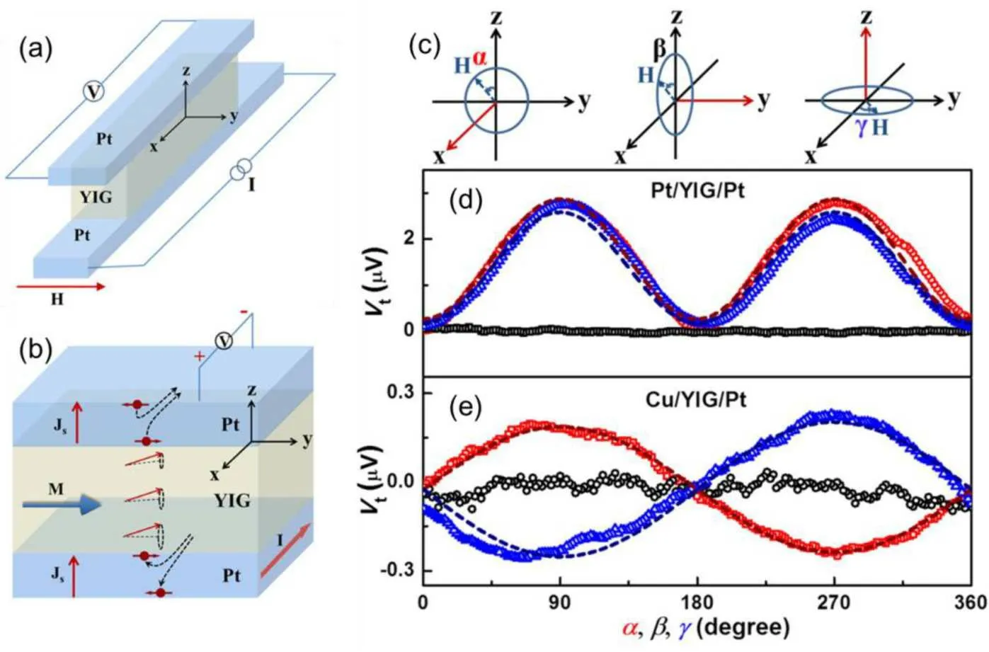
Fig.3. (a)Measurement setup for the MECD effect. (b)Schematics for the MECD effect: a current in the bottom Pt drags a voltage signal in the top Pt with the external field or the magnetization of YIG collinear with the polarization of current-induced spin current. In the YIG,there exists a magnon current which mediates the current drag effect. (c)Angle scanning definitions with current along the x axis. (d)Two-fold symmetry for the MECD in the Pt/YIG/Pt sample,and(e)360° symmetry for the spin Seebeck effect in the Cu/YIG/Pt control sample.[50]
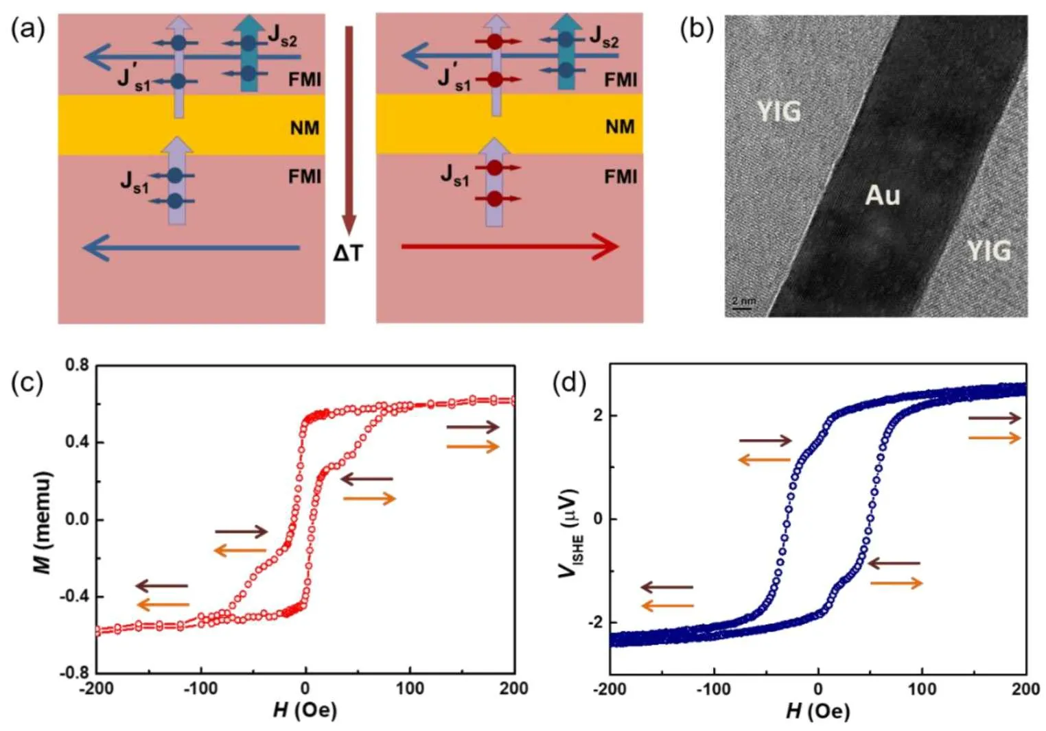
Fig. 4. (a) Schematic diagram of magnon valve effect in FMI/S/FMI heterostructures, where a temperature gradient is applied to generate the magnon current by spin Seebeck effect. (b)High-resolution transmission electron microscopy image of YIG/Au/YIG heterostructures. Panels (c)and (d) show the magnetization and inverse spin Hall voltage as a function of magnetic field, respectively, which demonstrates the magnon valve properties.[60] The unit 1 Oe=79.5775 A·m-1.
While the MECD effect and SSE can produce magnon current,another issue,how to manipulate magnons or magnon currents,arises. In order to regulate magnon currents,Wu[60]and Guo[61]et al.invented magnon valves and magnon junctions, respectively, as shown in Figs. 4 and 5. These devices share a common structure that consists of an MI/spacer/MI(MI/S/MI) sandwich. For the magnon valves (junctions),the spacer layer is served by a nonmagnetic metal (antiferromagnetic insulator) layer. Analog to the spin valves whose resistance is high or low depending on their antiparallel or parallel magnetization states,respectively,these magnon valves/junctions can also output high or low magnon current in the SSE when magnetizations of the two magnetic insulators are aligned in parallel or antiparallel manner. This phenomenon is named as the magnon valve effect (MVE)[60,62]and magnon junction effect(MJE).[61,63]The involved physics is simple: the detected magnon current on the top MI is not only determined by the SSE of itself but also depends on the transmitted magnon current from the bottom MI. Thus, the measured voltage is proportional to the sum or difference of the magnon currents produced in the top and bottom MI layers in the SSE, depending on the magnetization state of the two MI layers.
Especially, for the magnon junction consisting of MI/antiferromagnetic insulator (AFI)/MI, the magnon junction effect (MJE) observed in it manifests that the SSE is essentially a bulk effect which cannot only be explained by physics at the interface with the top MI layer and the AFI can also function as a magnon-current channel and the magnon relaxation length of the typical AFI materials NiO and CoO are about 3.5 nm–4.5 nm at 100 K–200 K and 3.4 nm at 300 K,respectively, as shown in Fig. 5. Especially, bulk CoO has a closer N´eel temperature to room temperature than NiO,which probably makes the CoO-based MJE has a better performance than the NiO-based one around 300 K.[64]

Fig. 5. The magnon junction and magnon junction effect (MJE) in YIG/NiO/YIG/Pt (a) and YIG/CoO/YIG/Pt (b) structures. The corresponding field-dependence of the magnetization states(c)and the output spin Seebeck voltage for the magnon junction(d).[61,63]
Meanwhile, some other elementary magnon devices are also invented. For example, Cramer invented the magnonspin valve using a YIG/CoO/Co heterostructure.[64]Here a spin current is pumped out from YIG into CoO/Co by ferromagnetic resonance and spin pumping effect of YIG and the detected ISHE voltage in Co depends on relative orientation between YIG and Co. The signal is attributed to different spin Hall angles of majority and minority spins in Co. Another style of magnon transistors,the lateral YIG/Pt structure is demonstrated.[65]On top of a YIG substrate, three Pt electrodes are deposited and function as source, drain and gate,accordingly. The MECD effect between the source and the drain can be controlled by a DC current applied in the gate.The above works have been summarized by Wright.[66]
In order to better understand the mechanism of magnon transmission and magnon junction effect (MJE) in magnon junction from the micro scale,Yanet al.studied magnon transmission and magnon blocking effect (MBE) in the sandwich structure of ferromagnetic insulators(FMI),antiferromagnetic insulators(AFI),and ferromagnetic insulators(FMI)by atomistic spin-model simulations,[67]as shown in Fig. 6. It is shown that both MVE and MJE can be reproduced in this work, demonstrating the magnetization-dependent magnon transmission. The MVE is stemmed from the polarization of the spin wave. In general, the spin-up (spin-down) lattices can only accommodate right-(left-)handed circularly polarized magnons. While only right-handed circularly polarized magnons are favored in FMI with upward magnetization,both left- and right-handed circular polarizations are permitted in AFI owing to two spin-opposite lattices.[68]This selection rule thus makes the total reflection of spin wave occur when magnons try to diffuse into a spin lattice,which does not support their polarization. For instance, when right-handed circular magnons excited in spin-up region are injected into the spin-down region, the selection rule would result in low magnon transmission across the interface. This phenomenon called magnon blocking effect(MBE).[67]

Fig.6. Simulated magnon transmission in magnon junction. (a)Illustration of the introduced temperature distribution and magnon potential.(b)Magnon potential (δ|Mz|) as a function of layer of P state, AP state, and FMI1|AFI system. (c) Separated channel-dependent δ|Mz|. (d) and (e) Schematics of spin-dependent magnon blocking of P and AP states respectively.[67]
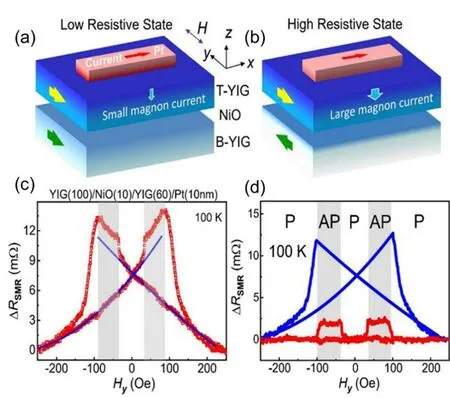
Fig.7. Schematics for the magnon-mediate nonlocal SMR effect for(a)parallel and (b) antiparallel states. (c) Field-dependence of the resistance of a YIG/NiO/YIG/Pt magnon junction. (d)Decomposition of the field dependence of resistance into an ordinary SMR effect(blue)and magnon-mediated nonlocal SMR(red).[63]
Besides of the MVE and MJE driven by the thermal SSE,the magnetic states of a magnon junction can also be read out by an electrical method via the so-called magnon-mediated nonlocal spin Hall magnetoresistance (MNSMR) effect,[69]as shown in Fig. 7. The classic SMR effect is usually observed in a MI/HM bilayer, for example, the typical YIG/Pt system.[70]The spin current produced in the Pt is absorbed via spin-transfer torque by YIG or transits into a magnon current inside YIG when polarization of the spin current is vertical or parallel to the YIG magnetization, respectively. The two physical processes result in different reflecting spin current back into the Pt layer, which then influences the resistance of Pt via the ISHE.For the MNSMR,instead,the resistance of Pt is diverse when a magnon junction below is in the parallel or antiparallel states and spin polarization is collinear with magnetization. This means the magnon junction has different magnon-sink performances when configured as parallel or antiparallel. Worth of noting, distinguished from the MVE in which magnon-current generation and transport are both involved, only magnon-current transport is involved for the MNSMR effect, manifesting magnon-transport controllability of a magnetic junction by its magnetic states.
Furthermore, recent progress has shown that one can use current-induced spin current or magnon current to transfer spin torque (spin-transfer torque/STT or magnon-transfer torque/MTT) to manipulate or even switch magnetization of magnetic insulators.[71,72]For example, Avicet al.[73]and Guoet al.[74]have switched magnetizations of TmIG and YIG using current-induced spin–orbit torques, respectively.Wanget al.designed a Bi2Se3/NiO/NiFe structure in which spin current produced in Bi2Se3can be converted into magnon current in the thick NiO spacer and finally switch in-plane magnetization of NiFe.[71]Meanwhile, Guoet al.designed a p-YIG/NiO/Pt heterostructure in which the YIG is not only insulating but also has perpendicular magnetic anisotropy,[72]as shown in Fig. 8. The magnon current in NiO converted from a spin current produced in Pt can switch perpendicular magnetization of YIG with help of an in-plane magnetic field. And the switching chirality, the clockwise or counterclockwise feature of the current dependence of perpendicular magnetization, depends on the direction of the in-plane field,which is a typical characteristic for thez-type SOT switching and rules out the entanglement from the in-plane Oersted field. Besides, the YIG is insulating, ruling out the possibility of electron tunnelling between a spin-current source and a magnetic layer. These experiments solidate the physics of the MTT effect. The above electrical writing and reading methods make the magnetic insulators and magnon valves/junctions a promising candidate for magnonic memory applications in a magnonics way.

Fig.8. (a)Measurement geometry for SOT and MTT-induced magnetization switching experiment. An external field parallel to current is necessary.(b)Measured current-dependence of anomalous Hall resistance Rxy for a YSGG//YIG/Pt sample. (c)Schematics for the MTT effect: A spin current in Pt transforms into a magnon current in NiO and is then absorbed by YIG with perpendicular magnetic anisotropy. (d)The current-dependence of Rxy for the YSGG//YIG/NiO/Pt heterostructure. Opposite external field results in opposite switching directions,which is a feature of the z-type SOT switching.[74]
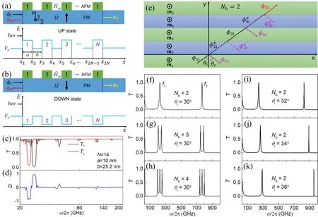
Fig.9. Magnon resonant transmission(MRT)effect and magnon resonant tunneling(MRT)effect in magnonic crystals(MCs). Panels(a)–(d)show the magnon resonant transmission effect in a one-dimensional MC. Panels (a) and (b) are the schematic diagrams of the MC in UP and DOWN states,respectively. (c)Calculated magnon transmission spectra in UP(T↑)and DOWN(T↓)states. (d)Difference between T↑and T↓. Panels(e)–(k) show the magnon resonant tunneling effect in an MC constructed by the periodic heterojunction when the incident angle exceeds the critical angle(θi >θc). (e)The magnon transmission in YIG(m1)/GdIG(m2)/YIG(m3)/GdIG(m4)/YIG(m5)with the P configuration. Nb represents the number of GdIG barriers. Panels(f)–(h)are the transmission spectra at θi=30° with Nb=2,3,and 4. Panels(i)–(k)are the transmission spectra at Nb=2 with θi=32°,34°,and 36°.[84,85]
In magnonics, the magnonic crystal (MC) is one of the most important structures and can be used to manipulate magnon transmission. MCs are the artificial media with periodic lateral variations in magnetic properties,[75–78]being analogous to the photonic and sonic crystals. The magnon spectra in MCs have the band structures containing band gaps, significantly different from those in uniform media. Magnons are scattered by multiple interfaces in MC and some of magnons with certain frequencies can completely pass through the MC when the resonance condition is satisfied, called the magnon resonant transmission (MRT)effect[79–81]or magnon resonant tunneling(MRT)effect.[82,83]Here, the similarity between the two effects is that the transmittance is equal to 1 (T=1) when the resonance effect occurs. The difference is that the evanescent waves exist in the resonant tunneling effect, while the there is no evanescent waves in the resonant transmission effect. Xinget al.have designed a one-dimensional MC constructed by the ferromagnet and periodic antiferromagnets as shown in Figs.9(a)–9(d), and found the magnon resonant transmission effect.[84]In Fig. 9(c), the peaks whereT↑= 1 (orT↓= 1) represent that the magnon resonant transmission occurs. The position and number of resonant peaks depend on period numberN, AFM widtha, and the distancebbetween two adjacent AFMs. Figures 9(e)–9(k) show the magnon resonant tunneling effect in an MC constructed by the periodic heterojunction YIG/GdIG.[85]Figure 9(e) illustrates the heterostructure YIG(m1)/GdIG(m2)/YIG(m3)/GdIG(m4)/YIG(m5), corresponding toNb=2,whereNbrepresents the number of GdIG barriers. Spin waves are in the form of plane waves in all the YIG layers, however, spin waves are evanescent waves in all the GdIG layers. In Figs. 9(f)–9(h), asNbis increased, the number of resonant tunneling peaks increases. In Figs. 9(i)–9(k),asθiis increased,the resonant tunneling peaks are moved to higher frequency.
Furthermore, Yanet al.theoretically studied the scattering behavior of spin waves at the interface of an antiferromagnetically coupled heterojunction.[86]It is shown that the SWs passing through the interface are evanescent waves and the incident waves are all reflected,demonstrating a magnetizationdependent magnon blocking effect(MBE)in this structure,as shown in Fig. 10. The theoretical result indicates that with the increase of the spin-wave frequency, the decay length decreases and the evanescent wave are more concentrated at the interface,showing a magnon skin effect(MSE)which is similar to the skin effect of electromagnetic waves.[87]

Fig.10. Magnon skin effect(MSE)in an antiferromagnetically coupled heterojunction. (a)Illustration of the spin-wave scattering at the interface of bilayer.Decay length of evanescent spin-wave beam under various frequency and incident angles for (b) spin waves injected from YIG into GdIG (YIG →GdIG)and (c) GdIG into YIG (GdIG →YIG). (d) Intensity map obtained from micromagnetic simulation of spin-wave scattering at the interface of FMI bilayer.Panel(e)is the partial enlarged detail of the interface as marked by the black square in panel(d). The evanescent spin-wave beam is marked by the red square.(f)–(i)Analytical and simulated evanescent waves.[86]
3. Conclusion and perspective
In this review, we give a comprehensive summary for the research areas from microelectronics, spintronics and magnonics.We mainly focus on the recent research progresses for the novel electrically-driven magnonic devices based on the magnon heterojunctions with vertically stacked layers in China: magnon-mediated current drag effect (MCDE),magnon valve effect (MVE), magnon junction effect (MJE),magnon blocking effect (MBE), magnon-mediated nonlocal spin Hall magnetoresistance (MNSMR), magnon-transfer torque (MTT) effect, and magnon resonant tunneling (MRT)effect, magnon skin effect(MSE),etc., laying the foundation for the future magnon-based logic,memory,and circuits.

Fig.11. Number of publications of magnon and magnonics-related research works from 1930 to 2022(not include all).
If we compare the emerging of spintronics and magnonics with the sophisticated microelectronics (Fig. 1), we think the spintronics and magnonics are still in a premature status. Figure 11 shows the number of publications of magnon,magnonics,and magnon spintronics-related research works from 1930 to 2022: for a long time before 2000,the research of magnonics keeps a stationary state and has a rapid increase especially after 2010, indicating the research hotspot and abundant opportunities for the magnonics. Prospectively, an era for spintronics and magnonics is blooming on the way. However,there are still many challenges remaining for uncovering novel magnon related quantum effects and inventing new magnon devices to read/write/process/control the spin/magnon current:firstly, the phase degree of freedom of magnons is still to be explored for magnonic devices,which is promising for the future quantum computing;secondly,the integration of magnon devices with CMOS for micro/nano electronic applications;thirdly,the new material and structures with ultralow damping for low-power magnon devices;and so on.
Acknowledgments
Project supported by the National Key Research and Development Program of China(Grants No.2017YFA0206200),the National Natural Science Foundation of China (Grant Nos. 51831012 and 12134107), and the Beijing Natural Science Foundation(Grant No.Z201100004220006).
猜你喜欢
中国典型病例大全(2022年13期)2022-05-10
小学生优秀作文(中年级)(2021年9期)2021-11-23
故事大王(2021年2期)2021-02-04
当代工人(2020年17期)2020-10-09
华人时刊(2019年21期)2019-05-21
艺术评论(2019年9期)2019-01-26
——献给新的一年
中国火炬(2016年1期)2016-11-28
民间故事选刊·上(2016年6期)2016-06-17
民间文学(2015年11期)2015-12-08
- Chinese Physics B的其它文章
- A design of resonant cavity with an improved coupling-adjusting mechanism for the W-band EPR spectrometer
- Photoreflectance system based on vacuum ultraviolet laser at 177.3 nm
- Topological photonic states in gyromagnetic photonic crystals:Physics,properties,and applications
- Structure of continuous matrix product operator for transverse field Ising model: An analytic and numerical study
- Riemann–Hilbert approach and N double-pole solutions for a nonlinear Schr¨odinger-type equation
- Diffusion dynamics in branched spherical structure