
Negative magnetoresistance in Dirac semimetal Cd3As2 with in-plane magnetic field perpendicular to current
2023-09-05 08:48HaoNanCui崔浩楠GuangYuZhu祝光宇JianKunWang王建坤JiaJieYang杨佳洁WenZhuangZheng郑文壮BenChuanLin林本川ZhiMinLiao廖志敏ShuoWang王硕andDaPengYu俞大鹏
Chinese Physics B 2023年7期
Hao-Nan Cui(崔浩楠), Guang-Yu Zhu(祝光宇), Jian-Kun Wang(王建坤), Jia-Jie Yang(杨佳洁),Wen-Zhuang Zheng(郑文壮), Ben-Chuan Lin(林本川),4,†, Zhi-Min Liao(廖志敏),‡,Shuo Wang(王硕),4,§, and Da-Peng Yu(俞大鹏),4
1State Key Laboratory for Mesoscopic Physics and Frontiers Science Center for Nano-optoelectronics,School of Physics,Peking University,Beijing 100871,China
2Shenzhen Institute for Quantum Science and Engineering,Southern University of Science and Technology,Shenzhen 518055,China
3International Quantum Academy,Shenzhen 518048,China
4Guangdong Provincial Key Laboratory of Quantum Science and Engineering,Southern University of Science and Technology,Shenzhen 518055,China
Keywords: negative magnetoresistance,chiral anomaly,topological semimetals,quantum transport
1.Introduction
The classical Drude model gives a magnetic fieldindependent conductivity formulanq2τ/m, which only considers carriers’collective drift and collision.Actually,a magnetic field could bend the motion paths of charged particles by Lorentz force and tend to localize the carriers in cyclotron orbits, corresponding to ordinary positive magnetoresistance(positive MR) with, hereσ0contributes to the zero-field conductivity.[1]When it comes to quantum well or topological system, unusual MR occurs and is generally considered as a signature of peculiar mechanism within quantum transport background,[2]such as linear MR and negative MR.Both of them are not limited to magnetic materials in view of moment scattering or transmission.As an instance,except for the negative MR source of quenching the Kondo effect[3,4]or magnetic phase transition,[5]nontrivial Berry curvature could revise relativistic particles’motion equation and contribute giant negative MR in topological semimetals or insulators.[6,7]
The topological semimetal is an analogue to graphene in three-dimensional situation, e.g.,A3Bi (A=Na, K, Rb)[8]and Cd3As2.[9–12]Band crossing formed by atom orbit’s hybridization could be regarded as sources and drains of Berry curvature with higher degeneracy.Especially,Dirac semimetals are located at the center of phase transition to Weyl semimetals or strong/weak topological insulators.[13]Extra magnetic fields could break the time reversal symmetry and lift Dirac points to two-fold Weyl points.Considering the rectification of dynamic equation with Berry curvature,an extra axial current is induced by balancing charge pumping and intervalley relaxation, namely, chiral anomaly.[6,14]The negative MR induced by chiral anomaly is expected to be observed only in the longitudinal configuration with parallel electromagnetic fields, i.e., parallelBandI.Most angle-dependence experiments focus on out-of-plane magnetic fields, demonstrating positive MR transition with vanishing chiral anomaly.[15,16]For a sample above the substrate, out-of-plane and in-plane measurements own unequal symmetry or geometric configurations with collision paths of circling.Carriers’motion is related to the dimension and in-plane measurements could also provide additional insights,e.g.,planar Hall effect.[17,18]
In this article, we report a considerable negative MR response by applying in-plane orthogonal electromagnetic fields in the Dirac semimetal Cd3As2.The amplitude of negative MR reaches−16% at 1.5 K and persists with−1% at room temperature.Such robust negative MR surviving to 300 K rules out the possible mechanisms such as quantum interference and alignment of random moments.Percolating current paths induced by charge puddles and disorder due to the inhomogeneous nanostructure and lattice disorder of Cd3As2might be involved to produce such considerable negative MR.Our results indicate that the negative MR effect in topological semimetals involves synergistic effects of many mechanisms despite the chiral anomaly, even when the magnetic field is parallel to the current.
2.Experiment and method
The Cd3As2nanowire is synthesized by chemical vapor deposition(CVD)method and transferred to silicon wafer with 285 nm SiO2oxide layer.Typical electron beam lithography technique is adopted to evaporate metal electrodes of Ti/Au with 10/200 nm.It is worth to note that the electrode regions are etched by Ar+before evaporation to reduce Schottky barrier and form Ohmic contact.Figure 1(a) shows an image of Cd3As2nanowire growing along[112]crystal direction by scanning electron microscope (SEM).The quantum transport measurements are conducted by Oxford cryogenic refrigerator with the lowest temperature of 1.5 K.Traditional four-terminal configuration is used for measurement and lockin amplifier SR830 provides alternating current with the amplitude∼100 nA and frequency∼17.777 Hz.
3.Results and discussion
Due to gapless energy bands around high degeneracy points and low density of relativistic Dirac fermions, thermal activation dominates the high temperature dependence of resistance.Metallic behavior appears after thermal energy is insufficient,[16]demonstrating a semiconductor-likeR–Tin Fig.1(b).By tuning the carrier’s density with backgate voltageVgat 1.7 K, a flat resistance kink is observed around−30 V, corresponding to the Dirac point in Fig.1(c).The asymmetry feature indicates different carrier mobility and Fermi velocity in our Cd3As2sample.Then,we focus on the main findings about negative MR under in-plane orthogonal electromagnetic fields as shown in Fig.1(d).MR is calculated by[R(B)−R(0)]/R(0)×100%.Either electron(Vg=0 V)or hole (Vg=−40 V) side reveals negative MR feature, achieving maximum of−10% around 2–3 T.In addition, the value of negative MR is−16% when the Fermi level is closed to the Dirac point(Vg=−30 V),which means surface states and compensation of charges might dominate transport channels since bulk states are almost gapped with a lack of free particles.This novel negative MR is unlikely ascribed to the chiral anomaly, since here the magnetic field is in-plane orthogonal to the current.Besides, current jetting[19]with uneven density distribution along with the sample could also be excluded by considering the sample spanned by electrodes,i.e.,uniform current injection.

Fig.1.(a) Image of Cd3As2 nanowire captured by SEM.(b) Temperature dependence of resistance probed by typical four-terminal configuration.(c)Back-gate voltage dependence of resistance at 1.7 K.Dirac point is marked around −30 V with a flat kink.(d)MR tuned by gate voltage with the magnetic field in-plane orthogonal to the current at 1.7 K.
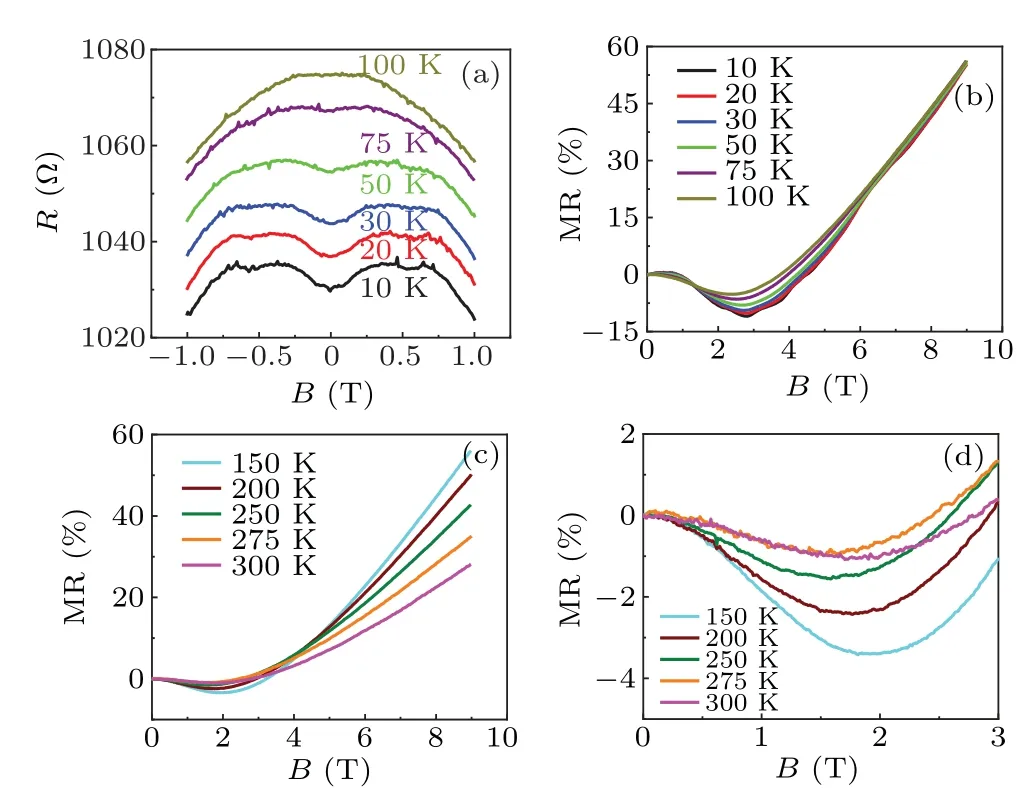
Fig.2.(a)Magnetic field dependence of resistance from 10 K to 100 K under 1 T at the gate voltage Vg =−30 V,showing possible WAL feature with resistance dips around 0 T at lower temperature.(b) and (c)MR curves from 10 K to 300 K.(d)The enlarged area of(c)in order to observe the MR value and kink position clearly.All the measurements are taken at Vg=−30 V.
Subsequently, the temperature dependence of the negative MR with perpendicular in-plane magnetic field and current is measured from 10 K to 300 K atVg=−30 V.A resistance dip is obviously observed around 0 T at 10 K, and gradually vanishes with increasing temperature to 75 K in Fig.2(a).This low temperature behavior might be relevant to weak anti-localization (WAL) with nontrivial extra Berry phase suppressing of backscattering in semimetals.[20]All the amplitudes of negative MR achieve the extrema under 3 T,with−11% at 10 K and decreases gradually by approaching room temperature, as shown in Figs.2(b)–2(d).The negative MR unlikely comes from weak localization (WL) since the value is considerable at all the selected temperatures,even persisting to 300 K with−1%.Quantum interference, such as WAL and WL,[21,22]is very sensitive to phase coherence length,which diminishes quickly with increasing temperature and could hardly exist at 300 K.[20]The reason is that the dephasing process is usually dominated by inelastic collisions,i.e.,electron–electron and electron–phonon scatterings,which implies higher temperature could enhance the relevant collisions and smear the quantum interference.
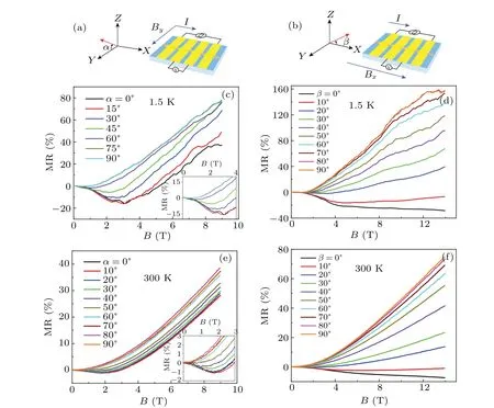
Fig.3.(a),(c),(e)Angle dependence of MR at 1.5 K and 300 K with orthogonal configuration of the magnetic field and the current.The insets reveal the MR at small magnetic fields.(b),(d),(f)Angle dependence of MR at 1.5 K and 300 K with parallel configuration of the magnetic field and the current,corresponding to the typical chiral anomaly in topological semimetals.All the measurements are taken at Vg=−30 V.
Angle-dependence experiments are further conducted by applying the magnetic field alongy–zplane andx–zplane respectively, corresponding toByvertical toIwithα=0◦andBxparallel toIwithβ=0◦, as shown in Figs.3(a)and 3(b).Similar with earlier negative MR reports in semimetals,[15,16]Figs.3(b), 3(d), 3(f) indicate a series of negative MR-topositive MR transition with rotation contrasts from in-plane to out-of-plane at 1.5 K and 300 K, demonstrating a significant result of chiral anomaly in our Cd3As2device.The maximum ofβ=0◦negative MR could reach−28%(1.5 K)and−7%(300 K) at 14 T, respectively.It is worth to note that negative MR curves have no trend to positive MR by increasing the magnetic field,distinguishing from breakdown ofC4rotation symmetry in Cd3As2.[16,21,23]This might be attributed to different energy band’s stability by CVD growth method, or sufficient orbital-dependent parth1compared with the mass term.[8]The key finding of negative MR with orthogonal electromagnetic fields also indicates a process of gradual disappearance by rotatingByto out-of-plane according to Figs.3(a),3(c), and 3(e).The insets amplify small field regions of the MR curves.It is interesting that the critical angles of negative MR-to-positive MR transition in orthogonal configuration are larger than he parallel ones, with 60◦(1.5 K),50◦(300 K)in former and 20◦(both 1.5 K and 300 K) in later.In addition,small angle misalignment of magnetic fields induced by measurement errors could be excluded as an origin of the negative MR in vertical in-plane magnetic fields by considering comparable values of the negative MR with parallel counterparts.Specifically,the negative MR ofα=0◦(−16%)is even larger than the normal chiral anomaly ofβ=0◦(−12%)in 3 T according to Figs.3(c)and 3(d).
We could conclude that the novel negative MR with orthogonal electromagnetic fields is insusceptible to carrier types and still survives at room temperature.Metallic behavior in low temperature phase of Fig.1(b)excludes strong localization or variable range hopping[24]as the origin of negative MR in the Anderson localized system.[25]The fact of lower intrinsic carriers around Dirac points is contradicted with skippingorbit effect observed in InSb films,[26]which claims classical surface boundary scattering brings to negative MR.Our results also rule out the conventional chiral anomaly with parallel configuration of fields in semimetals.Next,we discuss the possible mechanism of the observed MR in this work.Topological surface states provide spin–momentum locking for Fermi loops under time reversal symmetry of two-dimensional surface Hamiltonian.Extra fields could shift loops and cause a net spin-moment polarization, either through current density or Zeeman fields.[27]Earlier works[28,29]have proven that ion milling such as Ga+or Ar+could induce local magnetic moments by introducing disorder and lead to spin-dependent scattering process between surface and bulk states.Indeed,our Cd3As2nanowire is fabricated by Ar+to form Ohmic contact as well, but only in electrode regions.It might not be possible that moment polarization-related scattering with disorder in such small areas covered by electrodes is able to cause an appreciable negative MR,[27]especially compared with the whole sample surface area.Besides, if net current brings spin polarization by spin–momentum locking,it seems that the relative direction of current and magnetic field should significantly influence the value of negative MR,[30,31]which is contradictory to our results.
In fact, such orthogonal configuration of negative MR is detected by an out-of-plane magnetic field in topological semimetals or insulators by several groups.[32–35]Percolating current path[32]induced by Zeeman energy is studied in theory and formed in abundant disorder bulk states.This perspective provides a possible mechanism for our negative MR results in the situation of vertical in-plane magnetic field and current.According to Fig.1(c), we could roughly estimate electron’s mobility withµ=×,[16]whereG,l,Care the conductance, sample’s length and the capacitance of SiO2.The mobility is only around 5040 cm2·V−1·s−1at electron side, which is relatively small.[10]Thus the disorder due to intrinsic Cd vacancies or anisotropy of lattice should be considered.[9]Such defects might cause the Coulomb potential fluctuation among charge positions.Besides,the cross section of Cd3As2nanowire is inhomogeneous due to its threedimensional tetragonal crystal structure and might be tapered around tips.[36,37]Carriers’ motion is restricted with varying dimension and might cause discrete energy level such as quantum confinement.Due to large Land´e factorg ∼40 in Cd3As2,[38]the Zeeman energy could provide an extra shift of electron clouds and bend current paths, causing the unexpected negative MR.
Although our negative MR is not detected by the out-ofplane magnetic field,it is related to specific simulation parameters of crystals, like different orientations of unit cells and Land´e factors.The competition with orbit-related positive MR might also smear the mechanism.Nevertheless,the spatial disorder and distorted current paths exist in our sample, which would necessarily involve conductivity fluctuation[39–41]or carrier puddles.[32]In the meantime,microscopic disorder islands,anisotropy of lattice and Fermi velocity need to be carefully investigated in further research.
4.Conclusion
In summary,we display a distinct negative MR result with in-plane magnetic field orthogonal to the current in the Dirac semimetal Cd3As2.The amplitude of negative MR could reach−16% around 1.5 K and persist to room temperature.Moreover, such a phenomenon is different from the conventional chiral anomaly induced negative MR,demonstrating the complexity of the origins of negative MR in quantum transport.Here the extra conductance channels may play important roles due to percolating current paths,charge puddles and large Zeeman energy in disordered samples.Our results indicate the synergistic effects of chiral anomaly and other possible mechanisms such as disorders or percolating current path,Berry curvature, etc.in the negative MR effect observed in topological semimetals.
Acknowledgements
This work was supported by the National Natural Science Foundation of China (Grant Nos.12004158, 12074162,and 91964201), the National Key Research and Development Program of China (Grant Nos.2022YFA1403700 and 2020YFA0309300), the Key-Area Research and Development Program of Guangdong Province, China (Grant No.2018B030327001), Guangdong Provincial Key Laboratory (Grant No.2019B121203002), and Guangdong Basic and Applied Basic Research Foundation (Grant No.2022B1515130005).
猜你喜欢
华人时刊(2022年7期)2022-06-05
中学生学习报(2021年15期)2021-10-20
Chinese Physics B(2021年5期)2021-05-24
当代工人(2019年20期)2019-12-13
都市生活(2019年6期)2019-08-07
福建中学数学(2018年1期)2018-11-29
美与时代·美术学刊(2018年4期)2018-06-21
水动力学研究与进展 B辑(2018年2期)2018-05-14
中国公路(2017年14期)2017-09-26
校园英语·下旬(2014年12期)2014-10-21

- Chinese Physics B的其它文章
- Interaction solutions and localized waves to the(2+1)-dimensional Hirota–Satsuma–Ito equation with variable coefficient
- Soliton propagation for a coupled Schr¨odinger equation describing Rossby waves
- Angle robust transmitted plasmonic colors with different surroundings utilizing localized surface plasmon resonance
- Rapid stabilization of stochastic quantum systems in a unified framework
- An improved ISR-WV rumor propagation model based on multichannels with time delay and pulse vaccination
- Quantum homomorphic broadcast multi-signature based on homomorphic aggregation