
High-performance vertical GaN field-effect transistor with an integrated self-adapted channel diode for reverse conduction
2023-09-05 08:48SiyuDeng邓思宇DezunLiao廖德尊JieWei魏杰ChengZhang张成TaoSun孙涛andXiaorongLuo罗小蓉
Chinese Physics B 2023年7期
Siyu Deng(邓思宇), Dezun Liao(廖德尊), Jie Wei(魏杰), Cheng Zhang(张成),Tao Sun(孙涛), and Xiaorong Luo(罗小蓉)
University of Electronic Science and Technology of China,Chengdu 611731,China
Keywords: GaN field effect transistor,reverse conduction,integrated diode,turn-on voltage
1.Introduction
GaN power devices perform at high frequency, high efficiency and high power density in power conversion systems.[1–3]At present, GaN horizontal high electron mobility transistors (HEMTs)[4–6]have been successfully commercialized because the two-dimensional electron gas(2DEG)causes low on-resistance and low loss,but it is difficult to obtain a breakdown voltage (BV) higher than 1.2 kV.Vertical GaN devices could improve BV by increasing the thickness of the vertical drift region without increasing the chip area,and thus an improved power density and a reduced power loss can be achieved.Moreover, the peak electric field (Efield) of a vertical GaN device is far from the surface, and is less affected by traps or defects in the surface,thus achieving better reliability.Several vertical GaN devices have been reported,such as the current aperture vertical electronic transistor(CAVET),[7–9]the metal–oxide–semiconductor field-effect transistor(MOSFET)with a trench gate[10–12]and GaN vertical fin transistors.[13–15]
In practical power electronics applications, a freewheeling diode(FWD)is necessary to provide a reverse current flow path.[16]The inherent p–i–n diode in a vertical GaN MOSFET as a FWD has a high turn-on voltage(typicallyVF≈3 V),[17]and its bipolar effect also degrades the reverse conduction performance.Generally, a Schottky barrier diode (SBD) antiparalleled externally with a conventional MOSFET[18]can address the issue, but it increases the area and introduces extra parasitic inductance and capacitance, leading to increased power loss.To solve the above problems,vertical GaN transistors with an integrated unipolar diode are a better choice.[19,20]However,there are few reports on the related structures.
In this paper,a novel vertical GaN MOSFET with an integrated channel diode(CD-FET)is proposed to improve the reverse conduction performance,maintaining high performance in the on-state,blocking state and switching state.The reverse turn-on voltage(VF)of the proposed device is significantly reduced compared with that of a conventional MOSFET with an inherent body diode as a FWD.In addition, the integrated channel diode(CD)does not add an extra parasitic parameter.
2.Device structure and mechanism
Figure 1(a) shows a schematic section of the proposed CD-FET.Its main feature is the integrated CD under the trench source to realize reverse conduction.The vertical extended side of the trench source contacts with N-drift as the anode of the CD,and the other surface side is embedded in the P-base to avoid latch-up.Both the P-type barrier layer(PBL)and the P-shield layer are shorted with the source.The body diode(BD)acts as a FWD in a conventional MOSFET,as marked in Fig.1(b).

Fig.1.Schematic cross section of(a)the CD-FET and(b)a conventional MOSFET.

Fig.2.(a)States of the CD-FET and CD.Operation mechanism at(b)forward conduction and(c)reverse conduction for the CD-FET.(d)Blocking state for the CD-FET and conventional MOSFET.(e)CGD and CGS for the CD-FET.
ThetCHis the channel thickness of the CD andWJEFTis the distance between the PBL and the P-shield layer.The thickness of the AlGaN, PBL and P-shield layers is 80 nm,800 nm and 800 nm, respectively.The thickness of the Ndrift and P-base for the CD-FET and conventional MOSFET is 10 µm and 400 nm, respectively.Simulations have been carried out in Sentaurus TCAD,[21]and physics models are used to make the simulation accurate, for example, the doping dependence model,the Auger model,the Shockley–Read–Hall recombination model, the high-field saturation model,the piezoelectric polarization(strain)model and the avalanche(van Overstraeten) model.The effective electron mobility in the GaN N-drift region is set as 900 cm2·V−1·s−1[22]and the effective electron mobility on the sidewalls of the gate is set as 50 cm2·V−1·s−1,owing to the etch damage.[22]
Figure 2(a) illustrates the states of the CD-FET and CD.The trench source metal/Al2O3/GaN forms the metal–insulator–semiconductor(MIS)structure.Owing to the work function difference between the metal and GaN in the MIS,depletion region-1(DR1)is formed.Depletion region-2(DR2)is formed by the PN junction composed of the N-drift region and the PBL.AtVDS>0 andVGS>VTH,the CD-FET is in the forward conduction state,and DR1 and DR2 overlap to pinch-off the CD channel.In this case,the forward current flows via the inversion layer along the sidewall of the gate,as denoted by the red arrow in Fig.2(b).In the reverse conduction state, when|VDS|>VF,the depletion region narrows and the CD turns on in Fig.2(a).Thus, the CD provides a reverse current path as denoted in Fig.2(c).It is worth noting thatVFof the CD is much smaller than that of the body diode,because the on-state voltage of the PN junction is high for a wideband semiconductor.Figure 2(d) shows that the P-shield layer in the CD-FET alleviates E-field crowding at the corner of gate(O)in the offstate, compared with the conventional MOSFET.Moreover,the PBL and P-shield layer modulate the E-field distribution in the drift region,and the electric field between the PBL and P-shield weakens these so as to further improve BV.Furthermore,the P-shield layer also effectively transforms part ofCGDintoCGS,as shown is Fig.2(e),which effectively reduces the switching loss of the device.The 2DEG in the AlGaN/N-drift GaN interface acts as a current distribution layer to decrease the on-resistance.

Fig.3.(a)Electron concentration contours at different VDS.(b)Electron concentration distribution at the line AA′.(c)Conduction band energy along the CD lateral channel at different VDS.
3.Results and discussion
Figure 3(a) shows the electron concentration contour of the CD region at differentVDS.AtVDS=0 and−1 V,the depletion regions are merged and the CD is in the off-state as illustrated by I and II in Fig.3(a).The electron concentration in the CD channel is much less than the N-drift doping,Nd, of 1×1016cm−3as shown in Fig.3(b).The depletion regions narrow with decreasingVDS, and the current path is turned on as shown in III in Fig.3(a),with the highest electron concentration in the CD up toNd.VFis defined as the|VDS|atIDS=−100 A·cm−2, soVF=1.65 V.It is worth mentioning that the CD channel is pinched off at CD-FET forward conduction (VDS>0), as shown by IV in Fig.3(a).Figure 3(c)shows the extracted conduction band energy curves along the CD lateral channel.The barrier height (qϕB) along the CD channel increases with increasingVDS, which is affected by the depletion effect.WhenVDS>−1.65 V, the barrier prevents electrons from flowing toward the anode of the CD.AtVDS=−1.65 V, the electronic barrier disappears and the CD turns on.
Figure 4 shows the reverse conduction characteristic and the corresponding equivalent circuits for the CD-FET and conventional MOSFET.The non-junction CD as a FWD in the CD-FET turns on prior to the body diode, as shown in Fig.4(b), achieving a very lowVF.Therefore,VFof the CDFET is significantly reduced to 1.65 V from 3.24 V in the conventional MOSFET with a body diode as the FWD.

Fig.4.Reverse conduction characteristics of a CD-FET and a conventional MOSFET: (a) I–V curves and (b) equivalent circuit and current density distribution(@|VDS|=VF).
Figure 5 shows the gate charge characteristics of the two devices.The gate charge (QGD) of the CD-FET is 519 nC·cm−2, which is far less than the 1160 nC·cm−2of the conventional MOSFET.The reason is that the overlap area between the gate and drain is reduced by the P-shield layer(shorted to the source),and thus part of theCGDtransforms to theCGS,leading to a reducedQGDfor the CD-FET.QGDwill determine the switching loss.
Figure 6(a) shows the test circuit for simulation of the switching characteristic.The load inductance and load current used in the simulation are 10 nH and 100 A·cm−2, respectively.Figures 6(b)and 6(c)show the turn-on waveforms atRG=5 Ω and turn-off waveforms under differentRGvalues, respectively.Owing to the ultralowQGDfor the CDFET, much higher dV/dtvalues are obtained during switching.Therefore, the CD-FET contributes to a reduction in turn-on loss (Eon) and turn-off loss (Eoff) of 82% and 78%,respectively, compared with those of a conventional MOSFET.Meanwhile,the current and voltage oscillations decrease while the switching time increases with increasingRG.Figures 6(d) and 6(e) show the dependence of switching loss(Eswitch=Eon+Eoff) onRG, respectively.Compared with a conventional MOSFET,the CD-FET exhibits a low switching loss under differentRGvalues,and reduces the switching loss by 80% atRG=5 Ω.AsRGincreases, the difference in the switching loss between the two devices increases.

Fig.5.Gate charge characteristics and the test circuit for simulation.
Figures 7(a)and 7(b)compare the E-field distribution of the two devices at breakdown.The breakdown criterion is defined as whenIdreaches 0.1 A·cm−2.[23,24]For the CD-FET,the P-shield layer and PBL introduce new E-field peaks (atP1 andP2) and enhance the E-field strength in the drift region.Meanwhile, the P-shield layer alleviates E-field crowding at the bottom corner of the gate(O),leading to a reduced E-field at the gate corner, withEO=1.28 MV·cm−1even atVDS=1446 V,as illustrated in Fig.7(b).For the conventional MOSFET, E-field crowding results inEO=3.49 MV·cm−1,and premature breakdown occurs at BV=833 V in Fig.7(c).Table 1 summarizes the comprehensive performances of the two devices.Compared with the conventional MOSFET, the CD-FET exhibits high performance,including a high value for Baliga’s figure of merit(FOM=BV2/Ron,sp),lowVF,high BV and ultralowQGDand switching loss.
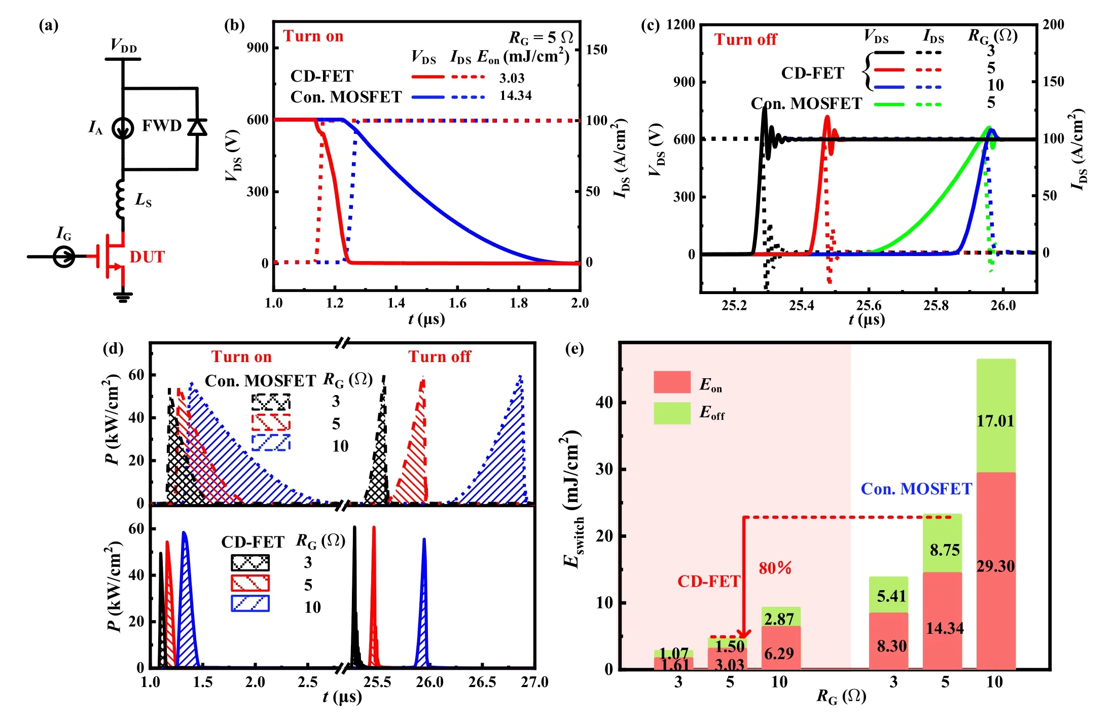
Fig.6.(a) Test circuit for simulation of the switching characteristic.(b) Turn-on waveforms at RG =5 Ω and (c) turn-off waveforms under different RG values for the two devices.Panels(d)and(e)compare switching losses of the two devices at different RG.
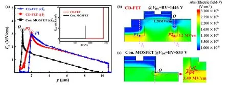
Fig.7.(a)The I–V curves,and Ey along l1,l2 andl3 at breakdown.E-field distribution at breakdown for(b)a CD-FET and(c)a conventional MOSFET.
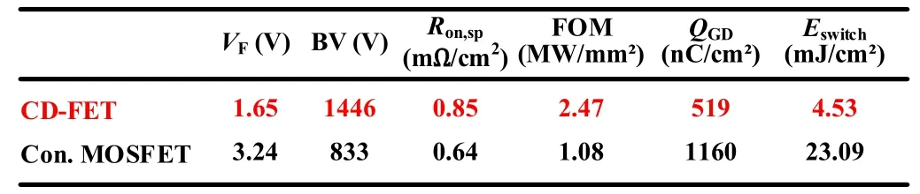
Table 1.Performance comparison of the two devices.
Fig.8.(a)Conduction band energy along the CD channel at different tCH.(b)Reverse conduction characteristics at different tCH.(c)Dependence of VF and BV on tCH.
Figures 8(a)and 8(b)show the influence oftCHon the reverse conduction characteristics.The increase intCHweakens the pinch-off effect, and thusqϕBandVFdecrease.Unfortunately, the leakage current in the CD channel is increased,and thus BV decreases, as shown in Fig.8(c).The device withtCH≤500 nm has a high BV which is less sensitive to change intCHbecause of the strong pinch-off effect.FortCH=600 nm,the CD channel fails to be pinched-off and the excessive leakage current leads to premature breakdown at 6 V withId=0.1 A·cm−2.It is worth mentioning thatRon,spis insensitive to the change intCHbecause the forward current of the CD-FET does not flow through the CD channel.
Figure 9 demonstrates the influences ofNPandWJFETonRon,sp, BV andVFfor the CD-FET.With increasingNP, the E-fields ofP1 andP2 increase (see Figs.7(b) and 7(c)), and the leakage current decreases owing to the enhancement of the pinch-off effect by the PBL,and thus BV increases.However,whenNP>5×1017cm−3,the high E-field ofP2 causes premature breakdown, and BV decreases asNPincreases.Ron,sphardly changes because the variation ofNPhas little influence on the long current path in the drift region.VFis constant because the pinch-off effect is strong enough and the CD is always in the off-state whenNP≥1×1017cm−3.The opening of the CD mainly depends on DR1 narrowing, as shown in Fig.3(a).With decreasingWJFET, the depletion effect for the junction field-effect transistor region is enhanced,the leakage current decreases in the off-state and thus BV increases.Meanwhile,the current path is narrowed in the on-state,leading to an increase inRon,sp.The opening of the CD channel is limited by the narrowertCH,soVFis constant.

Fig.9.Influences of WJFET and NP on BV and Ron,sp.
4.Conclusion
A vertical GaN FET with an integrated self-adapted CD is proposed to realize reverse conduction with a lowerVF.At forward conduction of the CD-FET,the CD is turned off without affecting the on-state characteristic.At reverse conduction,the CD turns on prior to the body diode, achieving a lowVF.Meanwhile, the PBL and P-shield layer modulate the E-field distribution to realize a high BV.The introduced P-shield also results in a much lowerQGD.Therefore,VF,QGDandEswitchof the CD-FET are decreased by 49%,55%and 80%,respectively,compared with the values for a conventional MOSFET.In addition, the CD-FET is beneficial for reducing parasitic inductance and the total chip area compared with the conventional method of using an externally connected SBD.
Acknowledgments
Project supported by the National Natural Science Foundation of China(Grant Nos.61874149 and U20A20208)and the Outstanding Youth Science and Technology Foundation of China(Grant No.2018-JCJQ-ZQ-060).
猜你喜欢
阅读(低年级)(2021年4期)2021-06-15
艺术品鉴(2020年9期)2020-10-28
爱你·阳光少年(2019年10期)2019-11-22
金山(2019年4期)2019-06-12
智富时代(2018年4期)2018-07-10
智富时代(2018年4期)2018-07-10
故事会(2016年4期)2016-02-19
女士(2015年6期)2015-05-30
37°女人(2014年4期)2014-03-13

- Chinese Physics B的其它文章
- Interaction solutions and localized waves to the(2+1)-dimensional Hirota–Satsuma–Ito equation with variable coefficient
- Soliton propagation for a coupled Schr¨odinger equation describing Rossby waves
- Angle robust transmitted plasmonic colors with different surroundings utilizing localized surface plasmon resonance
- Rapid stabilization of stochastic quantum systems in a unified framework
- An improved ISR-WV rumor propagation model based on multichannels with time delay and pulse vaccination
- Quantum homomorphic broadcast multi-signature based on homomorphic aggregation