
Optical anapole modes in hybrid metal–dielectric nanoantenna for near-field enhancement and optical sensing
2023-12-02 09:22DebaoWang王德宝JingweiLv吕靖薇WeiLiu刘伟YanruRen任艳茹WeiLi李薇XinchenXu许鑫辰ChaoLiu刘超andPaulChu朱剑豪
Chinese Physics B 2023年11期
Debao Wang(王德宝), Jingwei Lv(吕靖薇),†, Wei Liu(刘伟), Yanru Ren(任艳茹), Wei Li(李薇),Xinchen Xu(许鑫辰), Chao Liu(刘超), and Paul K Chu(朱剑豪)
1School of Physics and Electronic Engineering,Northeast Petroleum University,Daqing 163318,China
2Department of Physics,Department of Materials Science and Engineering,and Department of Biomedical Engineering,City University of Hong Kong,Hong Kong 999077,China
Keywords: light–matter interaction,metal–dielectric nanoantenna,anapole mode,electric field enhancement,optical sensing
1.Introduction
High-refractive-index dielectric nanostructures with low material loss and large mode volume[1,2]have attracted extensive attention and play crucial roles in enhancing local fields.By manipulating the interactions between light and matter,interesting optical phenomena such as Fano resonances,[3,4]radiation-free anapole mode,[5–7]and quasi-bound states in the continuum (BIC)[8]have been explored for the development of nonlinear optics,[9–11]sensors,[12–14]and surface-enhanced Raman scattering.[15]Current research activities are focusing on the generation of radiation-free optical states by promoting the interference between the different multipolar resonance modes in dielectric systems.At present, the excitation of radiation-free optical states can be summarized in two forms: the quasi-bound states in the continuum(BIC)[16]and the anapole mode.[5]Although both phenomena can be analyzed by the multilevel expansion theory,their underlying excitation mechanisms are inherently different as shown in three points below.Firstly, BIC is an intrinsic state of the system and does not subside with the disappearance of the incident light, whereas the anapole mode requires a specific structure to be designed as well as illumination by incident light to be excited.[17]Secondly,the BIC perfectly confines the energy to the boundaries without radiating it to the far field.[18]While the anapole mode can radiate energy into the far field and the destructive interference can occur in the far field.Thirdly,BIC can be used in biosensing applications due to their concentrated energy and hence higher quality factor and sensitivity.While the sensitivity obtained by the anapole mode is not comparable to that of BIC,but it can still be utilized as a sensor and offers the advantage of effectively addressing the limitation of BIC, especially the relatively low near-field electric field.Hence,the anapole mode is the primary option when explores the effects of the incident light on the scattering properties of nanoantennas.
The most representative multipolar interference is the electric dipole state induced by the combination of electric dipole moment (ED) and toroidal dipole moment (TD).Lvet al.had observed the electric dipole state in gallium phosphide nanodisks with forked slits and observed an electric field enhancement factor of 33.6.[19]Wuet al.had improved the near-field electric field inφ-shaped dielectric nanostructures based on the anapole mode giving rise to a field enhancement factor of 45.[20]In addition,similar studies had been carried out on complex structures such as meta-surface.Tianet al.had observed an electric field enhancement factor of 468 by offsetting the central disk at the disk-ring meta-surface.[7]Heet al.had studied silicon nanodisks with slots on the Ag substrate and the electric field enhancement was improved to 125.[21]Compared to similar dielectric nanostructures, the near-field enhancement of metal nanostructures comprising precious metals such as Au and Ag is significantly higher.[22]The collective oscillations of conducting electrons in the metal nanostructures upon excitation by an electromagnetic field can generate a high electric field attributable to localized surface plasmon resonance(LSPR).[23,24]In fact,metal nanostructures possessing LSPR properties also produce many interesting optical phenomena that are dependent on the shape,arrangement,and materials.[25]However, the high intrinsic loss leads to an increase in local temperature and energy absorption thereby limiting practical applications.
In order to overcome the drawbacks of metals and dielectrics,hybrid metal–dielectric nanostructures have emerged as an attractive platform to reduce ohmic losses and improve field enhancement.[26]Hybrid nanoantennas show the anapole mode in the dielectrics which can compensate for the material loss of metals.The LSPR properties of metals can be exploited to confine the strong electromagnetic field at the sharp metal tip.[26]However,despite recent progress,the field enhancement of hybrid metal–dielectric nanoantennas in the near-infrared region is only about tens or hundreds[20,27]thus requiring further improvement.Although excitation of the anapole mode can be realized in dielectric systems,[28,29]the physical mechanism of the anapole mode and coupling between the metal and dielectric are still not well understood.
Herein,a hybrid metal–dielectric nanoantenna consisting of six wedge-shaped gold (Au) nanoblocks as well as silica(SiO2) and silicon (Si) nanodisks is designed to excite the anapole mode and improve the near-field enhancement.The physical mechanism of the anapole mode is investigated by analyzing the characteristics of scattering and field distributions of the SiO2and Si nanodiscs.Based on the LSPR properties,the electric field enhancement is further improved by introducing an Au nanodisk to the dielectric surface.After conducting a comparative analysis of the scattering properties of the Au nanodisk splitting into different parts, it is observed that the structure with the gold nanodisk splitting into six wedgeshaped Au nanoblocks is capable of exciting and manipulating the anapole mode at multiple wavelengths.Furthermore,the electric fields at these operating wavelengths (AM1 and AM2) are enhanced.By optimizing the different parameters,the electric field enhancements at AM2 and AM2 are 518 and 1482,which are about 235 and 674 times than that of the original dielectric structure,respectively.Additionally,the nanoantenna is an excellent refractive index sensor with a sensitivity of 550 nm/RIU at AM2.Our results provide new fundamental knowledge about the excitation and manipulation of multiwavelength optical anapole modes and guidance to improve the local electric field.
2.Theory and model
2.1.Optical anapole mode
A simple doughnut-shaped model depicted in Fig.1 is adopted.The electric dipole moment (ED) is interpreted as a pair of charges with opposite polarity as shown in Fig.1(a).According to Fig.1(b),the toroidal dipole moment(TD)along the symmetry axis of the ring surface outward is related to the distribution of the polar electric field.The static magnetic field generated at the ring surface is concentrated in the coil in the form of circulating magnetic currents.As shown by Fig.1(c),the anapole mode consists of scattering of ED and TD with the same radiation pattern (equal in magnitude but opposite in phase) canceling each other in the far-field region, which manifests in the electric field profile as two circulating current loops.[17,30]The destructive interference in the far-field region improves the local field enhancement factor.The local field enhancement factor(LFEF)is defined as follows:
whereErepresents the local electric field andE0denotes the electric field of the incident light.

Fig.1.Schematic diagram showing excitation of the optical anapole mode.
2.2.Multipole decomposition
As a result of the polarized charge–current in the scattering medium, the process of light scattering can be considered re-emission of light.[31]The distributions of the polarized charge–current can be divided into three dynamic multipoles within the context of classical electrodynamics: electric multipoles, magnetic multipoles, and toroidal multipoles.[32]Therefore, the method of multipole decompositions including the electric dipole momentPα(ED), magnetic dipole momentMα(MD), toroidal dipole momentTα(TD), electric quadrupole momentQeαβ(EQ),and magnetic quadrupole momentQmαβ(MQ) can be utilized to analyze the scattering cross-section (SCS) and near-field characteristics of the nanosystem.The general expressions are described as follows:[31,33]
wherer,J, and the subscriptsα,β=x,y,zdenote the position vector, polarization current density excited in the antenna,and components of EQ and MQ,respectively.The term,D=P+(ik0εd)/cT, which is the total electric dipole moment (TED), is employed to characterize the interference of the electric dipole momentP(ED) and toroidal dipole momentT(TD)in the far-field region.[20]The radiation powerIconsisting of these multipoles can be determined by
whereω,candε0are the angular frequency, speed of light,and vacuum dielectric constant, respectively.The scattering cross-sectionCscais described as follows:[34]
whereIincis the radiation power of the incident light wave.
2.3.Structure and modeling
In the near-infrared region, Fig.2(a)presents the metal–dielectric nanoantenna consisting of six wedge-shaped gold(Au)nanoblocks as well as silica(SiO2)and silicon(Si)nanodisks.The three parts are arranged without gaps from top to bottom and the silica nanodisk which serves as a gain medium facilitates the near-field interactions by enhancing the coupling of both the metal and dielectric layers.[35,36]The hybrid nanoantenna is analyzed by the finite method(FEM).The plane wave is linearly polarized along thex-axis and propagates parallel to thez-axis(red symbols).The nanoantenna is placed in the air with a permittivity of 1.0.The refractive indexes of Au and SiO2are obtained from Palik’s handbook[37]and the refractive index of Si substrate is 3.5.The front view(X–Z)and top view(X–Y)of the nanoantenna are depicted in Figs.2(b) and 2(c) and the symbols, quantities, and units of the structural parameters are listed in Table 1.
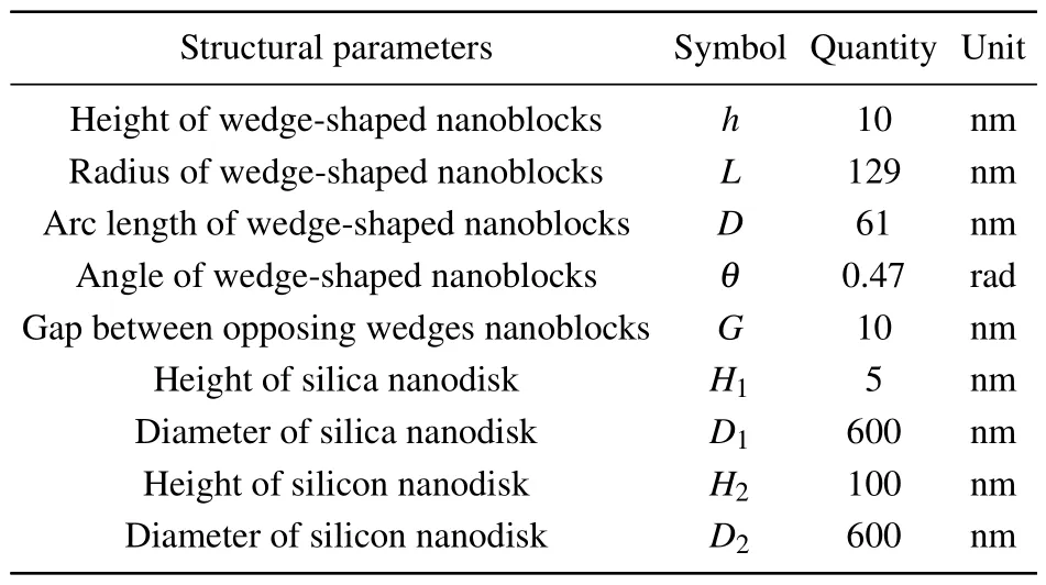
Table 1.Structural parameters of the nanoantenna.
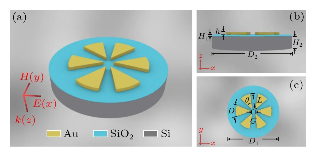
Fig.2.(a)Three-dimensional(3D)view,(b)front view,and(c)top view of the nanoantenna.
3.Results and discussion
3.1.Assembly of silica and silicon
To study the physical mechanism of the anapole mode,the combination of silica (SiO2) and silicon (Si) nanodisks is adopted in the initial configuration, which is the typical form for activating the anapole modes in practice, as shown in Fig.3.Silica and silicon nanodisks have the same diameterD1=D2= 600 nm and their heights are set toH1=5 nm andH2= 100 nm, respectively.Figure 3(b) shows the contributions of various multipoles to the scattering crosssection(SCS)for wavelengths between 1000 nm and 1800 nm.The SCS is dominated by the electric dipole moment (ED)and toroidal dipole moment (TD), while the other multipoles are negligible in comparison with these two moments.A clear dip at 1165 nm and corresponding dipole moments ED,TD, and TED are illustrated in Fig.3(c), which shows destructive interference between ED and TD and indicates the anapole arrangement.Owing to the anapole mode, SCS shows a minimum value of 0.15 µm2, while the local field enhancement factor (LFEF) shows a maximum of 2.2, as shown in Fig.3(d) (gradient color bar).Our analysis of the anapole mode is corroborated by the electric and magnetic field profiles in Figs.3(e) and 3(f).The hot-spot distribution is distinct for the electric and magnetic fields.That is, the electric hot spot is mainly in the center,whereas the magnetic hot spot is located on both sides.As shown by the dotted arrow, the main electric current at the resonance of the anapole mode is positioned at the center of the nanodisk and the weak currents are distributed on both sides thus producing two current loops.In particular, the current in the dielectrics stems from the oscillation of bound electrons due to field penetration and phase delay effects,which are fundamentally distinguishable from the conduction current produced by free electrons in metals.[19,38]
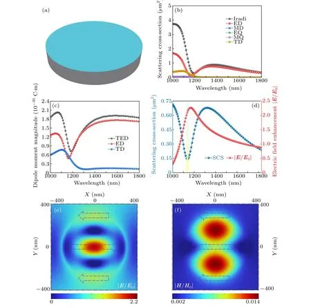
Fig.3.(a) Schematic diagram of the combination of silica and silicon nanodisks.(b) Contributions of different multipoles to the scattering cross-sections.(c) Dipole moments of ED, TD, and TED.(d) Electric field enhancement factors |E/E0| and scattering cross-sections versus wavelength.(e)Electric and(f)magnetic field distributions at 1165 nm.
3.2.Gold nanodisk
To obtain more near-field improvement,a gold(Au)nanodisk with a radiusL=129 nm and heighth=10 nm is added to the dielectrics to form a hybrid metal–dielectric nanostructure.The Au nanodisk is split on the dielectrics and the corresponding scattering cross-section (SCS) and local field enhancement factor (LFEF) are plotted in Fig.4.As shown in Figs.4(a)–4(d), the metal improves the field enhancement compared to the individual dielectrics due to LSPR.[39,40]The Au nanodisk in Fig.4(a) disrupts the anapole mode of the SiO2and Si assembly resulting in incomplete radiation cancellation in the far-field region for ED and TD.Consequently,the highest LFEF (wavelength of 1811 nm) does not coincide with the position of the minimum SCS (wavelength of 1706 nm).Moreover, the Au nanodisk shows a uniform division into two parts separated by a 10 nm gap, as shown in Fig.4(b).The SCS at 1247 nm shows a minimum value of 0.17 µm2, while the LFEF has a maximum value of 77.54 in agreement with the anapole mode characteristics.Figure 4(c)shows that the optical properties of the Au nanodisk are further divided into four parts.Compared with the Au wedge-shaped nanoblocks, the SCS and LFEF curves do not change significantly, but the LFEF weakens.This phenomenon can be ascribed to that the larger contact area of the nanoblocks results from further splitting.Therefore, electrons move to different regions to decrease the localized surface plasmonic effect in the central region.Particularly, in addition to the occurrence of the dips in the anapole mode,multiple scattering dips do not satisfy the feature of the anapole mode in which the LFEF acquires a maximum and the SCS acquires a minimum, while they result from the coupling of different resonance modes between the metal and the dielectric as well as the different interactions between light and matter in Figs.4(a)–4(c).Figure 4(d) presents the calculated results for splitting into six uniform wedge-shaped nanoblocks.A new anapole mode(named AM1)occurs at 1080 nm from the strong coupling between metals as well as metals and dielectrics.The original anapole mode(AM2)shown in Figs.4(b)and 4(c)blue-shifts to 1353 nm.In comparison with Figs.4(a)–4(c),the structure divided into six wedge-shaped nanoblocks show greater field enhancements in AM1 and AM2 of 170 and 680,respectively.The phenomenon can be explained by the accumulation of free electrons in the metal at the tip position of the wedge-shaped structure during light excitation, consequently improving the electric field.[41]Therefore,the nanostructure composed of the six wedge-shaped Au nanoblocks together with the SiO2and Si nanodisks is analyzed and optimized.
Fig.4.Schematic illustration on the right in panels (a)–(d) of the structure of the Au nanodisk splitting the dielectric assemblage and the corresponding curves of SCS and LFEF.
3.3.Optimization of structural parameters
Aside from the aforementioned structural configuration effects, the structural parameters play a crucial role in the properties of the nanoantenna.In our analysis, by fixing the other parameters, the two parameters, angleθ, and gapG,that have a large effect on the scattering cross-section (SCS)and local field enhancement factor (LFEF) are studied.Figures 5(a)–5(f) present the optimization process for different structural parameters of the wedge-shaped Au nanoblocks(θ,G).Exploration of the angular variation involves the control of a unique variable by maintaining a constant volume of 37500 nm3for each wedge-shaped nanoblock.According to Figs.5(a)–5(c), the SCS at AM1 tends to move in the direction of short wavelengths and decreases in value as the angleθchanges from 0.47 rad to 1.05 rad.As for AM2,the SCS shows a blue shift followed by a redshift, while the corresponding LFEF decreases and then increases due to the difference in the degree of aggregation of the tip polarization charge density caused by variation of the angle.[41]Figures 5(d)–5(f)describe the effect of the variation of the gap on the SCS and the LFEF.The SCS at AM1 blue-shifts,while at AM2,it blue-shifts first and then red-shifts because of the different degrees of interference of ED and TD.For both AM1 and AM2, the LFEF increases and then decreases.The reason is that the small gaps have limited effectiveness in inducing more electrons to move toward the tip,while large gaps hinder the excitation of free electrons.Considering the effects of the wedge-shaped structural parameters on the field enhancement and sensing properties, the optimal values areθ= 0.47 rad (arc lengthD=61 nm)andG=10 nm.
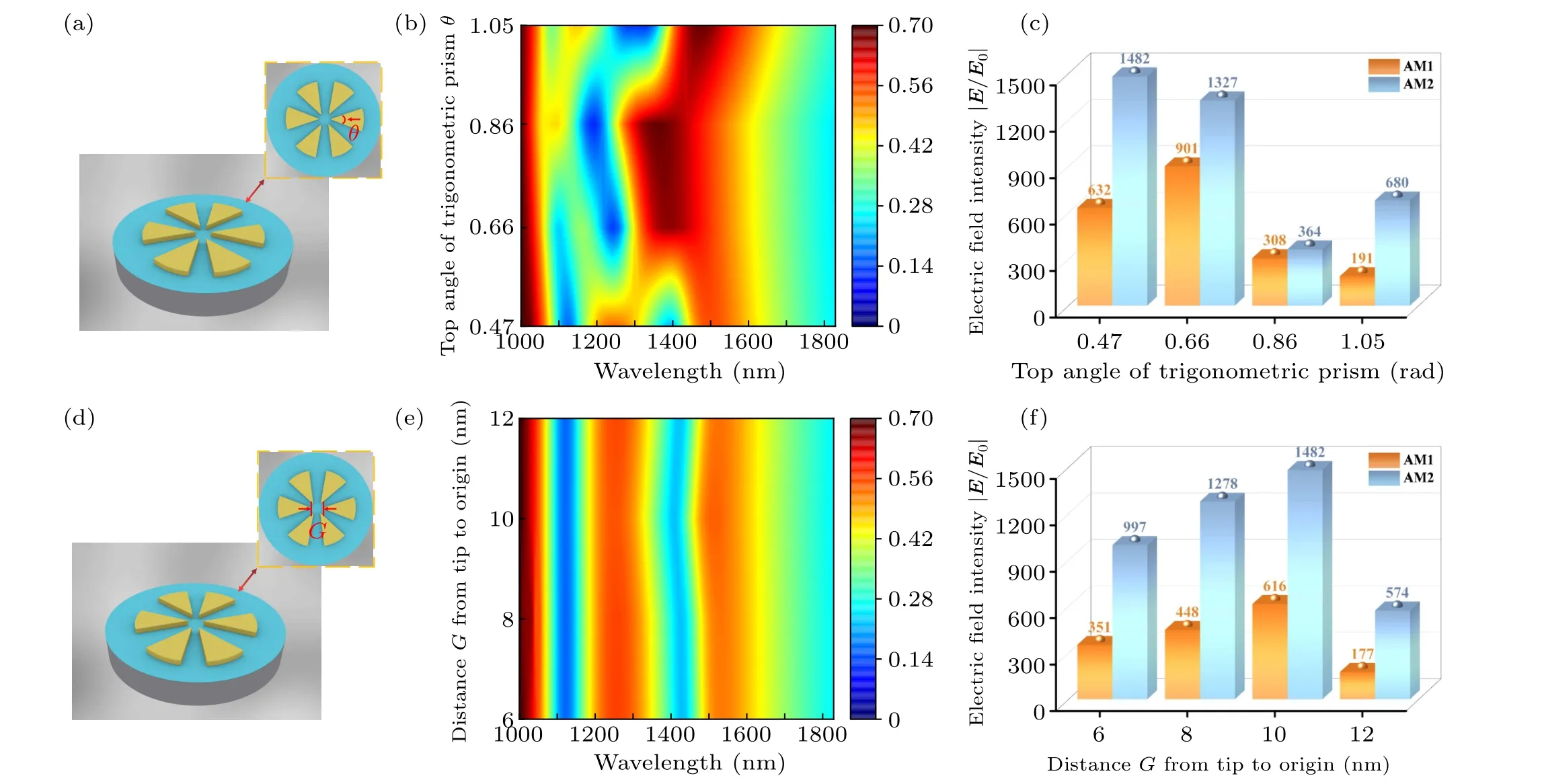
Fig.5.(a)and(d)Cross-sections of the wedge-shaped nanostructure for different θ and G.(b)and(e)Effects of parameter changes on SCS.(c)and(f)Effects of different gaps on LFEF expressed by 3D histograms.
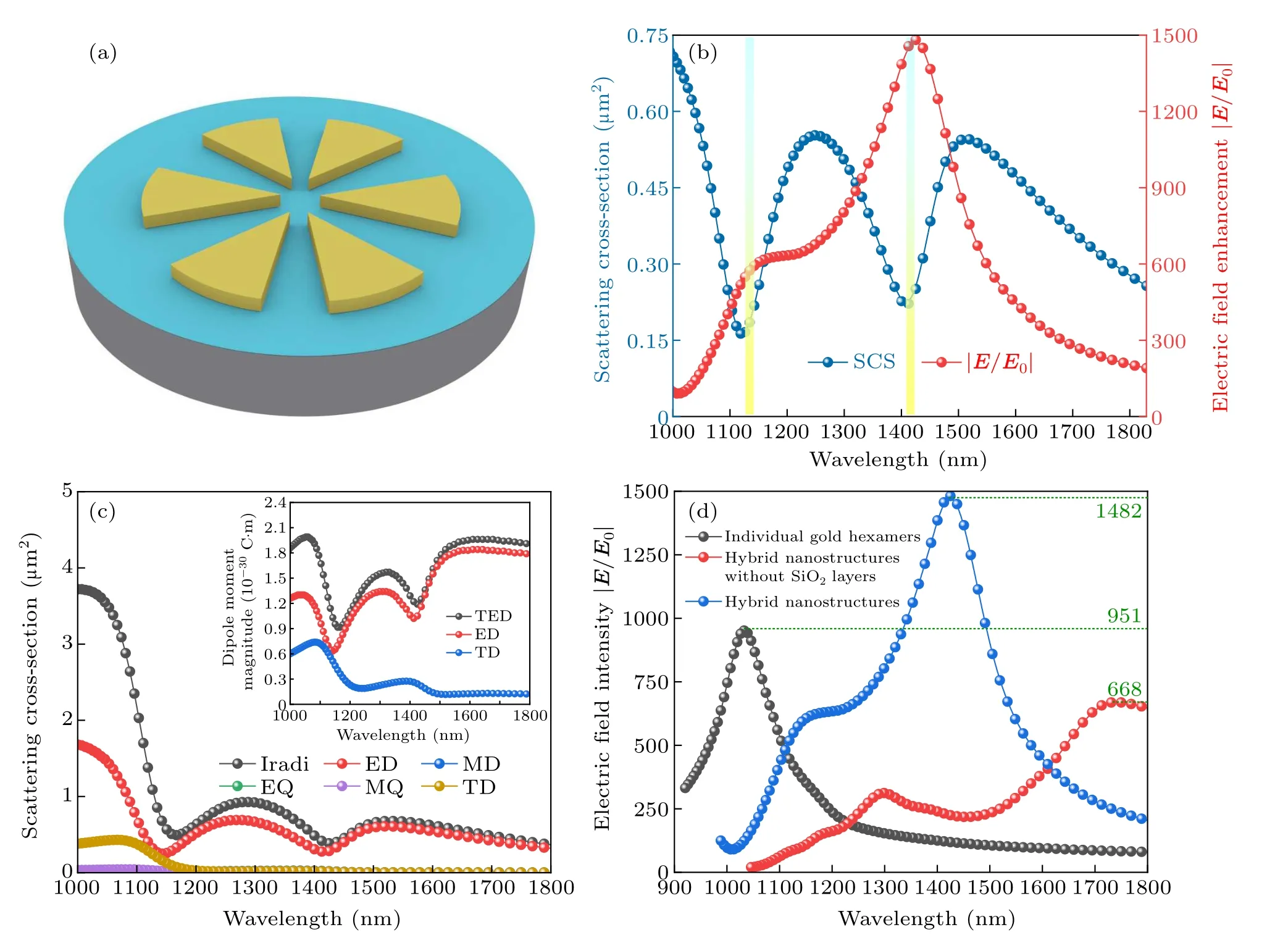
Fig.6.(a) Schematic diagram of the wedge-shaped hybrid nanoantenna.(b) Electric field enhancement factors |E/E0| and scattering crosssections as a function of the wavelength.(c)Cartesian multipole decompositions of the scattering spectra of the nanoantenna.(d)Comparison of electric field intensity|E/E0|of individual gold hexamer,hybrid nanostructure with or without SiO2 layer.And the inset in panel(c)represents the dipole moments of ED,TD,and TED.
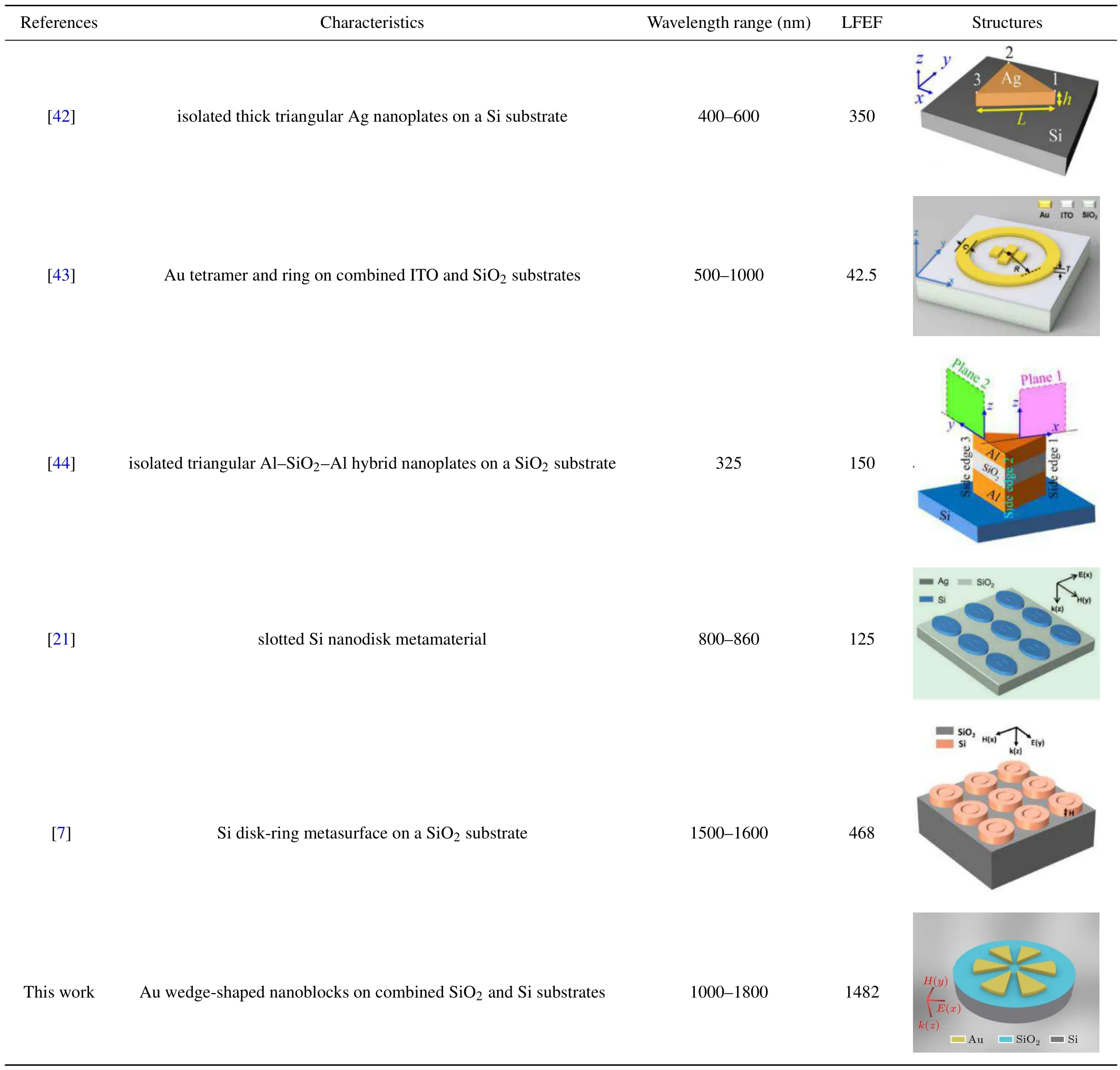
Table 2.Comparison of the electric field enhancement factor(LFEF)characteristics.
3.4.Anapole modes of the hybrid nanosystem
To elucidate the origin of the substantial increase in the electric field, the scattering characteristics are investigated(Fig.6).As shown in Fig.6(c), the scattering spectra are primarily dominated by the electric (ED) and toroidal (TD)dipole moments,while the contribution of the other multipoles is small and negligible.The ED dips(AM1 and AM2)occur atλ=1159 nm and 1425 nm on account of the destructive interference and spatial overlap of the ED and TD.[27]Hence, the strong coupling of metals and dielectrics can excite interesting optical modes for the specific structural configurations.The electric field enhancement factor(LFEF)and scattering crosssection (SCS) as a function of the wavelength are shown in Fig.6(b).The gradient color bars denote the wavelength positions of AM1 and AM2,and their characteristics are consistent with the principle of the anapole mode(Fig.1).At AM1,there is scattering transparency, and the corresponding SCS diminishes to approximately 0.15 µm2.The LFEF values at AM1 and AM2 are about 518 and 1,482,respectively,which are significantly higher than those of the original dielectric structure.Additionally,in order to illustrate the essential significance of the SiO2layer in metal–dielectric coupling,Fig.6(d)exhibits the electric field intensity|E/E0|of individual gold hexamer,hybrid nanostructures without SiO2layers as well as hybrid nanostructures.Obviously,the proposed nanostructure is significantly superior to the other two structures(the LFEF of 951 and 668).This result indicates the SiO2nanodisk which serves as a gain medium facilitates the near-field interactions by enhancing the coupling of both the metal and dielectric layers.
3.5.Electromagnetic field distribution
In order to provide a more visual representation of the optical characteristics of the anapole mode, theE-field andHfield distributions at AM1 and AM2(wavelengths of 1159 nm and 1425 nm) are presented in Fig.7.Under the effect of the boundary conditions and scattering field, the charge density in the middle gap region is obviously stronger,resulting in great near-field enhancement.Furthermore,the essence of the anapole mode is illustrated by the two symmetric circulating currents in the displacement current distribution (red marks)presented by the electric field, and the two typical hot spots are shown by the magnetic field.In order to confirm the superiority of our nanoantenna,Table 2 compares the properties of different nanoantennas.
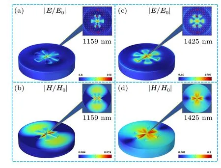
Fig.7.(a)and(c)Electric and(b)and(d)magnetic field distributions at AM1 and AM2(1159 nm and 1425 nm)with the red curves with arrows indicating the direction of the displacement current.
3.6.Refractive index sensing
The sensitivity (S) which is an important property of sensors[45]is described by[46,47]
where ∆λand ∆nrepresent the variation of the wavelength and change of adjacent refractive indexes,respectively.The comparison structure(single gold wedge nanoblocks deposited on dielectric substrates) and hybrid nanostructure are analyzed based on the variation at these dips as a function of the refractive indexes of the external environment between 1.0 and 1.5.The wavelength change has a great impact on the sensitivity.For comparison structure, as depicted in Fig.8(a)and Table 3, the AM1 and AM2 all move in the direction of long waves with the external refractive index increasing.The maximum sensitivity at AM2 is approximately 470 nm/RIU.But for hybrid nanostructure, as shown in Fig.8(b) and Table 3,both AM1 and AM2 show the increased variance of the wavelength by red-shifting(dark green arrow),but the effect is more pronounced at AM2.The maximum sensitivity at AM2 is about 550 nm/RIU, which is significantly higher than that of the comparison structure.This result indicates that our proposed structure has a higher sensitivity.A comparative analysis of representative optical sensors is presented in Table 4 and our sensor indeed delivers excellent performance.

Table 3.Sensitivity analysis of comparison structure and hybrid nanostructure.
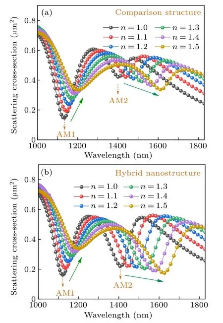
Fig.8.(a)Scattering spectrum of the comparison structure and(b)hybrid nanostructure at different refractive indexes.

Table 4.Comparison of the properties of our sensor with those of representative sensors recently reported.
4.Conclusion
A metal–dielectric nanoantenna composed of six wedgeshaped gold(Au)nanoblocks in conjunction with silica(SiO2)and silicon (Si) nanodisks is designed and investigated.The dielectric combination of SiO2and Si nanodisks is adopted to study the nature of the optical anapole mode.Excitation of multi-wavelength anapole modes and the local field enhancement factor(LFEF)is improved by introducing the split gold (Au) nanodisk to the dielectric surface.By performing optimization, the LFEF of the metal–dielectric nanoantenna increases to 518 and 1482 at AM1 and AM2, respectively,which are approximately 235 and 674 times higher than those of the initial dielectric structure.The nanoantenna can also be employed as a refractive index sensor with a sensitivity of 550 nm/RIU at AM2.The hybrid nanoantenna exhibits excellent enhancement in the near-field electric field and has excellent optical sensing properties,thereby providing the theoretical guidance for future applications pertaining to surfaceenhancement Raman scattering as well as optical sensing.
Acknowledgments
Project supported by the Outstanding young and middleaged research and innovation team of Northeast Petroleum University (Grant No.KYCXTD201801), the Natural Science Foundation Projects of Heilongjiang Province of China(Grant No.LH2021F007), the China Postdoctoral Science Foundation(Grant No.2020M670881),the Study Abroad returnees merit-based Aid Foundation of Heilongjiang Province of China (Grant No.070-719900103), the Northeastern University scientific research projects (Grant No.2019KQ74),the City University of Hong Kong Donation Research(Grant Nos.9220061 and DON-RMG 9229021), and the City University of Hong Kong Strategic Research (Grant No.SRG 7005505).
猜你喜欢
思维与智慧·下半月(2022年5期)2022-05-17
Chinese Physics B(2022年2期)2022-02-24
Chinese Physics B(2022年1期)2022-01-23
雷锋(2021年12期)2021-04-12
语数外学习·高中版中旬(2021年12期)2021-03-09
摄影与摄像(2020年11期)2020-09-10
小天使·五年级语数英综合(2019年8期)2019-08-27
艺术品鉴(见今)(2017年3期)2017-05-15
水动力学研究与进展 B辑(2017年6期)2017-03-14
当代音乐(下旬刊)(2016年5期)2016-05-30

- Chinese Physics B的其它文章
- Optimal zero-crossing group selection method of the absolute gravimeter based on improved auto-regressive moving average model
- Deterministic remote preparation of multi-qubit equatorial states through dissipative channels
- Direct measurement of nonlocal quantum states without approximation
- Fast and perfect state transfer in superconducting circuit with tunable coupler
- A discrete Boltzmann model with symmetric velocity discretization for compressible flow
- Dynamic modelling and chaos control for a thin plate oscillator using Bubnov–Galerkin integral method