
Low-damage photolithography for magnetically doped(Bi,Sb)2Te3 quantum anomalous Hall thin films
2023-12-02 09:22ZhitingGao高志廷MinghuaGuo郭明华ZichenLian连梓臣YaoxinLi李耀鑫YunheBai白云鹤XiaoFeng冯硝KeHe何珂YayuWang王亚愚ChangLiu刘畅andJinsongZhang张金松
Chinese Physics B 2023年11期
Zhiting Gao(高志廷), Minghua Guo(郭明华), Zichen Lian(连梓臣),Yaoxin Li(李耀鑫), Yunhe Bai(白云鹤), Xiao Feng(冯硝),2,4,5, Ke He(何珂),2,4,5,Yayu Wang(王亚愚),4,5, Chang Liu(刘畅), and Jinsong Zhang(张金松),4,5,§
1State Key Laboratory of Low Dimensional Quantum Physics,Department of Physics,Tsinghua University,Beijing 100084,China
2Beijing Academy of Quantum Information Sciences,Beijing 100193,China
3School of Integrated Circuits,Tsinghua University,Beijing 100084,China
4Frontier Science Center for Quantum Information,Beijing 100084,China
5Hefei National Laboratory,Hefei 230088,China
6Beijing Key Laboratory of Opto-electronic Functional Materials&Micro-Nano Devices,Department of Physics,
Renmin University of China,Beijing 100872,China
7Key Laboratory of Quantum State Construction and Manipulation(Ministry of Education),Renmin University of China,Beijing 100872,China
Keywords: topological insulator,quantum anomalous Hall effect,fabrication techniques
1.Introduction
Magnetic topological insulators(TIs)have attracted wide attention in condensed matter physics in the past decade.The intricate interplay between magnetic order and band topology gives rise to a variety of exotic topological quantum phenomena.[1,2]A prominent example is the QAH effect[3]that was first realized in Cr-doped (Bi,Sb)2Te3magnetic TI thin films grown by molecular beam epitaxy (MBE).As a contemporary version of the integer quantum Hall(QH)effect without magnetic field,[4,5]the QAH effect is characterized by a quantized Hall resistanceRyx ∼h/e2and a zero longitudinal resistanceRxx ∼0 at zero magnetic field, wherehrepresents the Plank constant andedenotes the elementary charge.Distinct from the integer QH effect that originates from the formation of Landau levels in strong magnetic field,[6]the QAH effect arises from the interplay between magnetic order and spin–orbit coupling,which opens an exchange gap at the Dirac point of the surface state.[7,8]When the Fermi level (EF) is tuned within the band gap, the QAH effect appears and the transport is carried by 1D dissipationless chiral edge state.[9,10]The realization of the QAH effect not only opens a new avenue for exploring exotic topological quantum physics,[11–20]but also holds great potential for practical applications, such as the low power consumption electronic devices,[9]topological quantum computation,[21,22]and metrology for quantum resistance.[23,24]
Since the first experimental observation of the QAH effect in Cr-doped (Bi,Sb)2Te3magnetic TIs,[3,11,12]the optimization of the QAH effect has become an important target in both condensed matter physics and material science.On the one hand,the adjustment of the sample growth conditions,such as by changing the magnetic dopant from Cr to V[25,26]or developing the magnetic modulation doping method instead of single doping,[26]can significantly enhance the observable temperature from 50 mK to 1 K.On the other hand,the continuously being discovered new materials such as MnBi2Te4intrinsic magnetic TI,[27,28]twisted bilayer graphene,[29,30]and AB-stacked MoTe2/WSe2heterobilayers[31]provide alternative routes to realize the QAH effect.In addition to the progress in searching for new materials, developing effective sample protection scheme represents another important direction in the study of the QAH effect.[32,33]However, in real experiment,even starting with the optimized materials,it does not guarantee that the fabricated device would retain its electronic properties as the original materials.The protective layer may also react with the chemical reagents during the fabrication process.In order to control and manipulate the dissipationless chiral edge states in functional electronic devices,artificially fabricating micro-structures by lithography are unavoidable.Therefore, considering the sensitivity of the electronic properties of TI films,[34,35]it is of great importance to develop a low-damage lithography method for magnetically doped(Bi,Sb)2Te3QAH films.
Previous researches on magnetic TIs along this direction mainly focused on the electron-beam-lithography (EBL), by which nanostructures down to tens of nm can be easily patterned.By developing low-damage EBL for nanostructures on Bi2Te3family TIs,various interesting quantum transport phenomena have been observed in experiment.[36–38]However,for another lithography method, the photolithography, which is more compatible with modern integrated circuit manufacture, its influence on the QAH behaviors has not been thoroughly explored.It is unclear whether the chemical reagents in photolithography would shift theEFposition or affect the magnetism.Therefore, it is highly desirable to develop lowdamage photolithography methods and perform control experiments on the influence of different fabrication methods on the properties of QAH thin films.Here, we have developed a low-damage photolithography method for magnetically doped (Bi,Sb)2Te3QAH thin films incorporating two resist layers of PMMA and AR-P 3740 (manufactured by AllResist),two commonly used positive resists in conventional EBL and photolithography, respectively.By measuring the transport behaviors of five QAH thin films fabricated by mechanical scratching,conventional photolithography with single resist, and modified photolithography scheme with two resists,we found that the new photolithography method enables the fabrication of QAH thin films with the transport and magnetic properties almost identical to those of the films fabricated by mechanical scratching.Our result represents a key step towards the production of novel micro-structured devices based on the dissipationless QAH chiral edge states.
2.Experimental details
The three QAH samples used in this study were 5-QL thick Cr/V doped (Bi,Sb)2Te3thin films grown by MBE on three SrTiO3(111)substrates following the recipes in our previous work.[19,25]Samples #1 and #2 were deposited with a 2-nm thick Al layerin-situin the MBE chamber at room temperature, which was then oxidized naturally into highly insulating AlOxwhen the samples were taken out of the MBE chamber [Fig.1(a)].The deposition of AlOxcan protect the QAH thin films from aging effect and is one of the most efficient methods for QAH sample protection.To explore the influences of photolithography on the transport properties,both samples#1 and#2 were cut into two pieces(#1-A,#1-B,#2-A,and#2-B).For samples#1-A and#2-A,Hall bar structures were mechanically scratched by hand using a sharp needle.For samples#1-B and#2-B,we adopted the conventional photolithography with single resist(AR-P 3740)and the modified photolithography method with two resists(PMMA and AR-P 3740),along with the etching method to pattern Hall bar structures(see the following paragraph for details).For sample#3,no capping layer was covered on the surface,which was used to determine the effect of heating on the transport properties.For transport measurements, a standard low-frequency fourprobe lock-in method was adopted with an excitation current of 200 nA at the frequency of 13 Hz.The SiTiO3substrate served as the gate dielectric due to its large dielectric constant at low temperature.The magnetic field was applied perpendicular to the film plane in a commercial He4refrigerator with the base temperature of 1.5 K.To eliminate the pick-up signals from geometrical misalignments,all the collectedRyxdata were antisymmetrized with respect to the magnetic field.
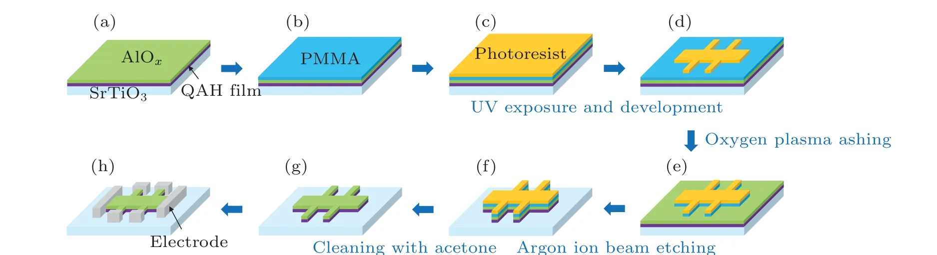
Figure 1 illustrates the schematic process of the modified photolithography method with two resists of PMMA and ARP 3740.We started by spin-coating the QAH thin films with a layer of 120 nm thick PMMA(marked by blue color)in an argon-filled glovebox with the O2and H2O levels lower than 0.1 PPM [Fig.1(b)].The sample was then transferred to a low-pressure environment pumped down to 5 Pa for 20 min to drive off excess resist solvent.Next,another 700 nm thick resist AR-P 3740(marked by yellow color)was coated on top of the PMMA layer [Fig.1(c)].Then the film was baked at 85◦C for 5 min to solidify the resists.After baking, the device was first exposed to a pattern of intense ultraviolet(UV)light with the dose of 55 mJ/cm2.In the next,the exposed area of AR-P 3740 was then dissolved by the sodium hydroxide developer for 20 s and rinsed with deionized water, leaving a Hall-shaped photoresist layer on the top of the PMMA layer[Fig.1(d)].Subsequently, oxygen plasma was employed to etch the PMMA layer [Fig.1(e)], with the Hall-shaped photoresist layer serving as a mask.The oxygen flow rate and pressure were controlled at 15 SCCM and 200 Pa, and the frequency and power of the radio-frequency field were set to be 13.56 MHz and 60 W.Although the AR-P 3740 layer also became slightly thinner during the oxygen plasma ashing process,the remaining layer was sufficient to serve as a mask during the etching of the PMMA layer.For the AlOxprotective layer and the QAH thin film, argon ion beam etching (IBE)with a beam current of 70 mA was employed at the rate of 15 SCCM and pressure of 2.2×10⁻²Pa[Fig.1(f)].After that,the sample was cleaned with acetone,rinsed with isopropanol and deionized water, and dried with nitrogen to remove the PMMA and AR-P 3740 resists completely[Fig.1(g)].Finally,electrical contacts were made by pressing indium pieces onto the films[Fig.1(h)].Commonly adopted deposition methods such as evaporation or sputtering can also be used for making electrodes.Compared to conventional photolithography, the modified method contains two additional steps of spin-coating PMMA and oxygen plasma ashing for the PMMA layer.
3.Results and discussion
To study the effect of standard photolithography on the properties of the QAH thin films, we first explored the magnetic field dependentRyxandRxxat various gate voltages(Vgs) for samples #1-A and #1-B, which were fabricated by mechanical scratching and conventional photolithography,respectively.Figure 2(a) displays the magnetic field dependentRyxandRxxfor sample#1-A.All the transport data shown in this work were taken at 1.5 K.The Hall traces exhibit wellsquared hysteresis loops, indicating the formation of longrange ferromagnetic order.AtVg=50 V,Ryxreaches the maximum value of 21.8 kΩ at zero magnetic field.Such high value ofRyxsuggests that the sample has already entered the incipient QAH state.[3]AsVgis moved away from 50 V,electronand hole-like carriers are injected into the sample.As a result, the zero-magnetic-fieldRyxis progressively reduced to 16.0 kΩ and 17.9 kΩ at-200 V and 200 V.The magnetoresistance curves exhibit the typical shape for a ferromagnet with two symmetric peaks at the coercive field.AtVg=50 V,Rxxreaches the minimum value of 20.1 kΩ at zero magnetic field,and increases to 41.6 kΩ at the plateau transition.To check if the conventional photolithography affects the transport properties of QAH thin films, we measured the transport properties on sample#1-B at the same conditions,with the data displayed in Fig.2(b).For sample #1-B, the shape of the Hall hysteresis is much less-squared than that of the sample #1-A.And the maximum value ofRyxis only as low as 3.3 kΩat 150 V,significantly reduced by nearly one order of magnitude.Meanwhile,the overall value ofRxxalso increases significantly,along with two broad and gentle peaks.These results clearly indicate the severe degradation of QAH sample quality during the conventional photolithography process.
In previous studies, people have already found that the QAH thin films are fragile and very sensitive to ambient conditions.[32–35]Therefore, a layer of AlOxis usually deposited on the surface to protect the sample from degradation.However, during the developing process of photolithography,the sodium hydroxide developer could react with the AlOxlayer and is also detrimental to the QAH films.To figure out this issue, we came up with the idea of adding an additional capping layer to isolate the AlOxlayer from directly contacting with the developer.In this case,the transport properties of the QAH films can be largely retained after fabrication.In order to verify our conjecture,we performed another control experiment on two QAH devices(samples#2-A and#2-B)obtained from one film, which were fabricated by mechanical scratching and modified photolithography,respectively.As shown in Figs.2(c) and 2(d), the Hall and magnetoresistance traces of the film by the modified photolithography(#2-B)show similar transport behaviors to those of the film fabricated by mechanical scratching (#2-A).The maximumRyxat zero magnetic field of sample#2-B reaches as high as 18.9 kΩ,only slightly lower than that of sample #2-A, which is 20.1 kΩ.The values ofRxxand their variation in magnetic field for negativeVgs of sample#2-B are very close to those of sample#2-A.Only a small decrease is observed inRxxfor positiveVgs, which is far away from the charge neutrality point.These observations strongly suggest that the modified photolithography with two resists is of low damage to the sample quality.

To amplify the different transport behaviors between the three fabrication methods, we extracted the values ofRyxat zero magnetic field and summarized its variation as a function ofVg.As shown in Fig.3(a),the conventional photolithography process not only reduces the value ofRyx, but also shifts the position ofEF.For sample #1-A,Ryxreaches the maximum at the charge neutrality point of around 50 V.However,for sample #1-B, theVgof the maximumRyxshifts to 150 V,indicating that the sample is p-doped during the photolithography.In contrast,for samples#2-A and#2-B,we found that theVgdependent transport data are almost overlapped.There is no obvious doping effect after the modified photolithography process.In Figs.3(c)and 3(d), we summarized the values of coercive field(Hc)as a function ofVgfor the two sets of data.The sharp contrast between the two curves in Fig.3(c)clearly demonstrates that the conventional photolithography scheme is detrimental to the properties of the QAH thin films.In contrast, the PMMA-protected photolithography method can largely keep the magnetism less affected by fabrication,as displayed in Fig.3(d).
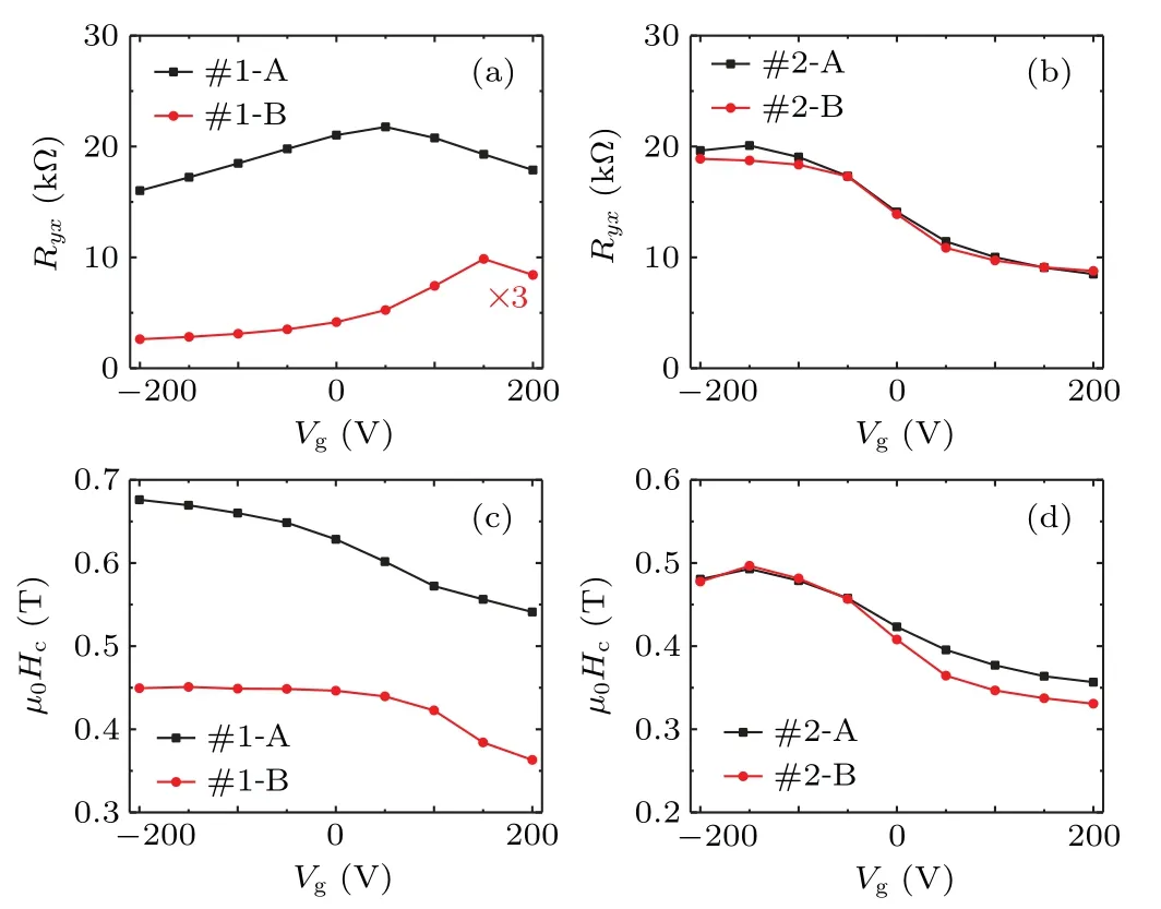
Fig.3.Comparison of transport and magnetic behaviors of the samples fabricated by different methods.(a)Vg dependent Ryx at zero magnetic field for samples #1-A and #1-B.The data for #1-B are multiplied by 3 for clarity.(b)Ryx at zero magnetic field as a function of Vg for samples#2-A and#2-B.(c)Vg dependent coercive field(µ0Hc)for samples#1-A and#1-B.(d)µ0Hc as a function of Vg for samples#2-A and#2-B.
Finally, we discuss a heating issue in the baking process during the lithography.In both EBL and photolithography,after the spin coating of the resist, a baking process is required to solidify the resist.The typical heating temperature for photoresist and e-beam resist ranges from 90◦C to 180◦C, and the baking time depends on the temperature and the thickness of resist,usually from 5 to 20 minutes.However,as displayed in Fig.4(a)for sample#3,Ryxdecreases from 18 kΩ to 11 kΩwhen the sample is heated at 90◦C in vacuum for 5 min, indicating that the properties of the QAH thin film are sensitive to heating and can be damaged at high temperature.Therefore,the up limits of baking temperature and time throughout our experiment are controlled to be 85◦C and 5 minutes.To make sure that both resists can be tempered enough at such a low temperature and a short total time,we conducted only one baking process after the spin coating of both resists.However,it brings in another issue that micrometer size holes appeared in the PMMA layer after the development of the photoresist.Figures 4(b) and 4(c) display the typical optical image of a fabricated device after the photoresist development and the atomic force microscopy (AFM) measurement result for the holes, respectively.We found that the depth of the holes is exactly the thickness of the PMMA layer, indicating that the holes run through the PMMA layer.Such result indicates that the sodium hydroxide developer can touch the film through these holes,making the protection ineffective.The appearance of the holes is attributed to the mutual dissolving of PMMA and AR-P 3740 due to the lack of baking of the PMMA layer before spin-coating AR-P 3740 photoresist.Exposure and development of the AR-P 3740 droplets in the PMMA layer give rise to the formation of holes in the PMMA layer,as illustrated in Figs.4(f)–4(h).To address this issue,we introduced a vacuuming process before spin coating of AR-P 3740, in which the pressure was reduced to 5 Pa for 20 min to solidify the PMMA layer.As shown in Figs.4(d) and 4(e), no obvious holes are observed in the optical image after the vacuuming process,and the AFM result displays a step edge with a height of 700 nm,which corresponds to the thickness of the photoresist.The schematic illustration of a device without holes is depicted in Fig.4(i).
4.Conclusion
In summary,we found that the conventional photolithography scheme with single resist cannot retain the properties of the original QAH thin film.Compared to the device fabricated by mechanical scratching,photolithography process reduces the Hall resistance and weakens the magnetic coercive field.By covering a layer of PMMA to isolate the protective layer of AlOxfrom the photoresist, we demonstrated that the PMMA-protected photolithography method enables the fabrication of QAH devices with the transport and magnetic properties almost identical to those of the pristine films.Our result represents a key step towards the production of microstructured electronic devices based on the dissipationless QAH chiral edge states.Additionally,this method could also be effectively applied to other sensitive two-dimensional thin film materials.
Acknowledgements
This work was supported by the National Key Research and Development Program of China (Grant No.2018YFA0307100), the Basic Science Center Project of the National Natural Science Foundation of China (Grant No.52388201), the National Natural Science Foundation of China (Grant Nos.12274453 and 92065206), and the Innovation Program for Quantum Science and Technology(Grant No.2021ZD0302502).Chang Liu was also supported by Open Research Fund Program of the State Key Laboratory of Low-Dimensional Quantum Physics (Grant No.KF202204).Yayu Wang was also supported by the New Cornerstone Science Foundation through the New Cornerstone Investigator Program and the XPLORER PRIZE.
猜你喜欢
交响-西安音乐学院学报(2021年1期)2021-05-29
开发研究(2020年2期)2020-07-30
水动力学研究与进展 B辑(2018年5期)2018-10-27
天津诗人(2017年2期)2017-11-29
红蜻蜓·低年级(2017年3期)2017-03-30
水动力学研究与进展 B辑(2015年5期)2015-11-25
小学生·多元智能大王(2015年5期)2015-05-25
新作文(小学中高年级版)(2015年5期)2015-04-12
红蜻蜓·低年级(2014年7期)2014-10-20
红蜻蜓·低年级(2014年3期)2014-07-09

- Chinese Physics B的其它文章
- Optimal zero-crossing group selection method of the absolute gravimeter based on improved auto-regressive moving average model
- Deterministic remote preparation of multi-qubit equatorial states through dissipative channels
- Direct measurement of nonlocal quantum states without approximation
- Fast and perfect state transfer in superconducting circuit with tunable coupler
- A discrete Boltzmann model with symmetric velocity discretization for compressible flow
- Dynamic modelling and chaos control for a thin plate oscillator using Bubnov–Galerkin integral method