
Electrical characterization of an individual nanowire using flexible nanoprobes fabricated by atomic force microscopy-based manipulation
2024-01-08 13:04YilinWangEnxiuWuJiruiLiuMengkeJiaRuiZhangandSenWu
纳米技术与精密工程 2023年4期
Yilin Wang,Enxiu Wu,Jirui Liu,Mengke Jia,Rui Zhang, and Sen Wu
AFFILIATIONS
State Key Laboratory of Precision Measuring Technology and Instruments,Tianjin University,Tianjin 300072,China
ABSTRACT Nanowires have emerged as promising one-dimensional materials with which to construct various nanocircuits and nanosensors.However,measuring the electrical properties of individual nanowires directly remains challenging because of their small size,thereby hindering the comprehensive understanding of nanowire-based device performance.A crucial factor in achieving reliable electrical characterization is establishing well-determined contact conditions between the nanowire sample and the electrodes,which becomes particularly difficul for soft nanowires.Introduced here is a novel technique for measuring the conductivity of an individual nanowire with the aid of automated nanomanipulation using an atomic force microscope.In this method,two nanowire segments cut from the same silver nanowire are positioned onto a pair of gold electrodes,serving as flexibl nanoprobes to establish controllable contact with the sample.By changing the contact points along the nanowire sample,conductivity measurements can be performed on different regions,thereby eliminating the influenc of contact resistance by analyzing multiple current–voltage curves.Using this approach,the resistivity of a 100-nm-diameter silver nanowire is determined to be 3.49×10⁻⁸ Ω m.
KEYWORDS Electrical characterization,Nanowire,Flexible nanoprobe,Nanomanipulation,AFM
I.INTRODUCTION
Over the past two decades,the fiel of nanodevices has surged,providing a new platform for studying diverse physical phenomena that are scientificall intriguing and technologically relevant.As ideal components for constructing nanodevices,1D materials in the form of nanowires have demonstrated many applications in nanoscale optoelectronic devices such as memristors,waveguides,and various sensors.1–4Therefore,a thorough understanding of the electrical properties of nanowires is critical for designing such devices,but precise characterization of the properties of individual nanowires is technically challenging because of their small size.
The typical way to measure the electrical properties of an individual nanowire is to connect it to two or four nanoelectrodes and obtain theIVcurves using an external electronic analyzer.The nanoelectrodes can be tungsten probes of nanomanipulators integrated into an SEM5or fabricated by electron beam lithography(EBL).6,7Because the former requires sophisticated equipment and operation skills,the EBL method is more commonly used.With EBL,the electrodes can be fabricated directly at any specifie position on the sample with well-controlled shape and size.However,a drawback of this method is that the exposure to chemical agents can introduce some defects or contamination into the sample,which in turn can cause ambiguous electrical measurements.8–11
To avoid chemical damage to the sample,the electrodes can be fabricated on another substrate by EBL firs and then transferred mechanically onto the measured material by PMMA.12–14However,this scheme requires high-precision alignment,which is sometimes tricky.Besides,after the transfer,the electrodes cannot be moved away,and so the sample cannot be reused or remeasured differently.
AFM is a powerful tool for manipulating samples with nanoscale precision,and a few groups have demonstrated the possibility of using AFM-based manipulation to move carbon nanotubes onto a pair of pre-produced electrodes for electrical measurement.15,16However,the contact resistances between the sample and the electrodes were not determined experimentally,thereby increasing the uncertainty of the measurement results.Moreover,the previous manipulation strategy was not designed for soft 1D materials and hence afforded poor control of the orientation and position of the flexibl nanotubes or nanowires,which also reduced the reliability of the measurement.
Recently,our group has developed an automated manipulation technique based on AFM,which is particularly suitable for manipulating flexibl nanowires.17–20Herein,we introduce this technique to improve the electrical measurement of silver nanowires.In our study,two silver nanowires were moved onto electrodes fabricated by PVD and used as a pair of flexibl nanoprobes to contact the sample.By adjusting the contact point along the nanowire sample,we obtained multipleIVcurves,whereupon the conductivity of the sample could be determined mathematically without knowing the contact resistance.The method and the experiment are described in detail in the remainder of this paper.
II.METHOD
A.Manipulation of a nanowire
Compared with rigid nanoparticles,flexibl nanowires are more difficul to manipulate because they may become severely deformed as they move.The in-plane deflectio of a nanowire under a lateral push forceFat its midpoint can be described by Euler’s beam model:17
whereEandIare the elastic modulus and sectional area moment of inertia of the nanowire,respectively,lis the initial length of the curved segment,qis the dynamic frictional force per unit length,and(x,y)are the coordinates of each point on the curved segment.Because the nanowire moves slowly and steadily,the pushing forceFis approximately balanced by the dynamic friction,i.e.,F≈ql.Therefore,Eq.(1)can be simplifie as
The controlled parameter in the AFM-based manipulation is the effective length of the push vector,i.e.,theycoordinate forx=0.Therefore,Eq.(2)can be converted to
which shows that the length of the curved segment is related to the deflectio at the push point,the mechanical properties of the nanowire,and the friction.
Herein,we propose manipulation strategies based on parallel push vectors(PPVs)to keep the nanowire straight after translation or rotation.As shown in Fig.1(a),a single push vector will cause part of the nanowire with lengthlto bend.The push point—which is the symmetric center of the bending part—has the maximum displacement equal to the length of the push vector.Two push vectors with an interval smaller thanlmay result in less curvature of the nanowire in between them.This is because the bending effects of the two vectors overlap,and the displacement at each point of the nanowire between the two push points is closer to the vector length.Therefore,if a group of PPVs with sufficientl small intervals as well as vector length are applied,the whole nanowire can be moved with an approximately straight shape.
Figure 1(b) shows the translation strategy.Assuming that the total length of the nanowire isL,the coordinates of its two ends are(0,0)and(L,0).For thenth push vector,the coordinates of the start point(Sn[X],Sn[Y])and the end point(En[X],En[Y])can be define as
where Δxis the distance between adjacent push vectors,Δyis the effective length of each vector,i.e.,the displacement(deflection of the sample at the push point,nis the vector number,which must be an integer ranging from 1 to 1+[L/Δx],Randrare the radii of the nanowire and the probe tip,respectively,andtis the recession distance,which is usually 10 nm or 20 nm.
The linearity of the nanowire after manipulation is essentially determined by Δxand Δy.Because the maximum linear errorelinalways happens at the midpoint between two adjacent push vectors,we can obtain the value of Δxby takingy(Δx/2)=Δy-elinin Eq.(3),and then the number of PPVs required to translate this nanowire by a distanceDcan be calculated with the round-up function,i.e.,
Figures 1(c) and 1(d) show the rotation strategy and the bending strategy,respectively,the latter of which can be considered as a special case of the former.In the rotation strategy,the middle point of the nanowire is set as the pivot,and the PPVs are central symmetric to this pivot.The length of each vector is proportional to the distance between the push point and the pivot.For a slight angle rotation,the coordinates of the start point and the end point of thenth vector are determined by the following equations:
For either half of the nanowire,the push vectors located farther from the pivot are executed with higher priority,because it is easier to rotate the nanowire from the ends.A more significan angular rotation can be realized by accumulating various slight angular rotations.As in the translation process,the nanowire is expected to reach the target direction and be re-straightened when all the PPVs are completed.
Given that in the translation strategy,the nanowire is always moved along the direction perpendicular to its major axis,we decompose the manipulation of moving a nanowire in any direction into three steps as shown in Fig.1(e).First,the nanowire is rotatedin situto the direction perpendicular to the line that connects its midpoint of the current position and the midpoint of the target position.Second,the nanowire is translated to the target position.Finally,the nanowire is rotated again to the target direction.
Apart from the strategies mentioned above,proper force and pushing speed are also critical for successful manipulation.A simplifie mechanical analysis of the contact between the AFM tip and the nanowire is shown in Fig.2.In Fig.2(a),FTP-NWandFNW-TPare the interaction forces between the tip and the nanowire,θis the angle betweenFNW-TPand the substrate,FNWadh,FNWsp,andfNWare the adhesion,support,and friction forces on the nanowire from the substrate,respectively,FTPadh,FTPsp,andfTPare the adhesion,support,and friction forces on the tip from the substrate,respectively,andFdefandFtorare the vertical and lateral forces on the tip due to the deflectio and torsion of the cantilever,respectively.IfFTP-NW⋅cosθ≤fNW,then the nanowire cannot be moved.Meanwhile,ifFNW-TP⋅sinθ>Fdef+FTPadh,then the tip will be jacked up and flippe over the nanowire.Therefore,to ensure reliable manipulation of the nanowire,the following conditions must be satisfied
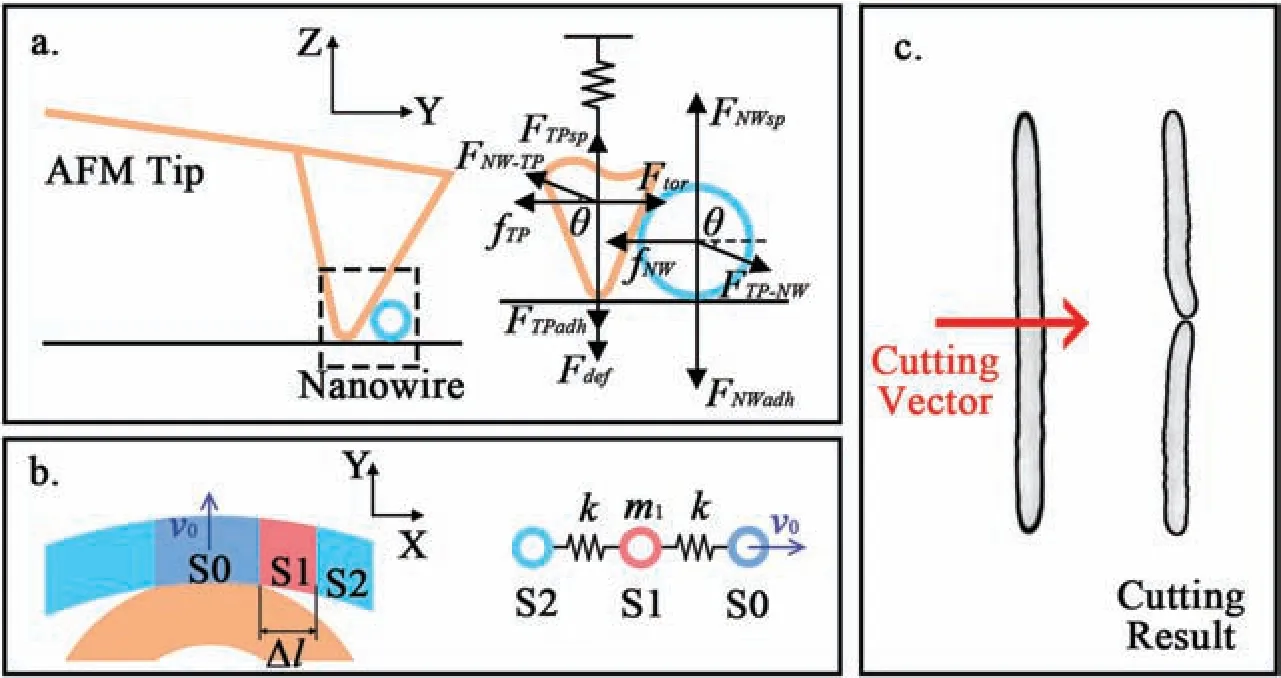
FIG.2.Schematics of manipulating a nanowire using a single push vector:(a)force analysis of probe tip and nanowire in YZ plane;(b)spring model of nanowire;(c)strategy for cutting a long nanowire into two nanowire segments.
Because the values ofFTP-NWandFNW-TPare equal andFdef≫FTPadh,the above conditions are simplifie as
which indicates that the nanowire can always be moved by lowering the probe’s height to provide a sufficien vertical pressure on the tip.
Figure 2(b) shows the local deformation of the nanowire around the push point.When segment S0—which directly contacts the tip—moves in theYdirection with speedv0,one side of its adjacent segment S1 is pulled by S0,and the other side of S1 is held by segment S2.To simplify the analysis,the nanowire segments S0–S2 are modelled as three rigid spheres connected by two springs with spring constantk.Setting the moment when S1 just starts moving ast=0,we have
wherem1andy1are the mass and displacement of S1,respectively,y0is the displacement of S0,andf1dandf1sare the dynamic friction force and the maximum static friction force between S1 and the substrate,respectively.Here,we suppose thatf1d≈f1s=f1.Given that the speed and displacement of S1 are both zero att=0,the solution of Eq.(9)is
The relative displacement between S0 and S1 is always larger than that between S1 and S2,with a maximum att=π/ω,i.e.,
Equation(12)only exists if no fracture occurs between S0 and S1,but asv0increases,Δymay exceed the yield limit of the nanowire.This result indicates that a nanowire can be cut by high-speed pushing as demonstrated in Fig.2(c).
So far,we have presented complete manipulation strategies for the translation,rotation,and cutting of nanowires,and by combining these strategies,we can manipulate nanowires freely and precisely.All the experiments presented in Sec.III were carried out using these strategies.Note that these manipulations included thousands of push vectors,which were generated by the Automan software developed by our group.By using this software,all the manipulation steps were implemented automatically and continuously without intermediate scanning,which significantl improved the experimental efficiency
B.Electrical measurement
Figure 3 shows schematically the electrical measurement principle.In Fig.3(a),W1 is the nanowire being tested,and P1 and P2 are two nanowires regarded as flexibl nanoprobes for contacting different areas of W1.Through P1 and P2,W1 is connected to a pair of gold pads fabricated by EBL,and the gold pads are connected to an external commercial electrical analyzer.The total resistance of the gold pads,the probe nanowires,and the contact resistance between them is considered as the internal resistanceRinof the electrodes.Therefore,the directly measured resistance from theIVcurves obtained by the electrical analyzer is
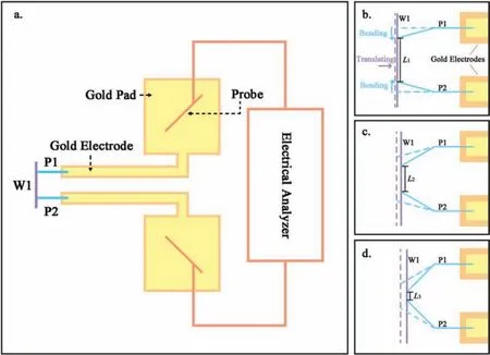
FIG.3.Schematics of measurement principle:(a)measurement schematic;(b)–(d)changing the contact positions of P1 and P2 with W1 by bending P1 and P2 and translating W1,where the length of W1 into the circuit is L1,L2,and L3,respectively.
whereRL1is the resistance of the nanowire W1 of lengthL1,andRC-Agis the contact resistance of P1 and P2 with W1.AlthoughRinandRC-Agare difficul to determine,they can be considered as constant if the contact condition is stable.
As seen in Figs.3(b)–3(d),the position and orientation of the nanowires can be changed by using the bending and translation strategies,thus changing the contact points on the nanowires.Then theIVcurve can be measured as the effective length of W1 is changed,and hence we haveR2andR3:
whereRL2andRL3are the resistances of W1 of lengthL2andL3,respectively.In this circuit,the contacts between the probe nanowires and the sample nanowire are always in the head-toside manner.21Therefore,RC-Agcan be considered as equal in Eqs.(13)–(15).By subtracting these equations in pairs,the change of measuring resistance ΔRcaused by the change of W1’s effective length ΔLcan be obtained.Suppose that the radius of W1 isr,then the resistivity of W1 can be calculated as
III.EXPERIMENTS
A.Sample preparation
The silver nanowires used in these experiments were produced by Nanjing XFNANO.They were dispersed in ethanol with a concentration of 40 μg/ml,and after 20 s of ultrasound,a solution droplet was deposited on the pre-processed wafer and allowed to dry naturally in the air.The silver nanowires on the substrate had a diameter of 100 nm and a length of 30–60 μm.
Figure 4(a) shows an optical view of the substrate with gold pads.The PVD method deposited a 220-nm-thick gold fil with arrays of square patterns on the silica surface.The gold patterns with a side length of 200 μm are the parts connected to the probes of the electrical analyzer during the following electrical measurement.Figure 4(b)shows an AFM image of the red box in Fig.4(a),which includes a long silver nanowire with a diameter of 100 nm.This long nanowire was cut into three segments and separated by the translation strategy as seen in Figs.4(c) and 4(d).Table I presents the parameters used in the manipulation process.The length of the two rightmost segments in Fig.4(d)was ∼13.5 μm,and they were chosen as the two probe nanowires,i.e.,P1 and P2.

TABLE I.Parameters of nanomanipulation.

FIG.4.Sample preparation process:(a)optical microscope image of substrate captured using a 5×objective;(b)AFM image showing a long silver nanowire with two cutting vectors executed to produce nanowire segments of specifi lengths;(c)result of cutting process,with the red arrows indicating the translation of each nanowire segment by a small distance to assess the outcome of the cutting experiment;(d)two nanowire segments were produced.
B.Construction of nanoprobes
Figure 5 shows the process of moving P1 and P2 onto the gold pads.These two probe nanowires were parallel to each other and aligned to the left to facilitate subsequent connection to the test nanowire.The 3D and section views confir that the probe nanowires were moved successfully onto the gold pads with good contact.
C.Connecting test nanowire in series with nanoprobes
Figure 6(a)shows the silver nanowire W1 moved near P1 and P2,where W1 was cut from another long silver nanowire ∼50 μm away and moved using the developed strategies.Figure 6(b)shows W1 connected to P1 and P2,while Figs.6(d)and 6(e)show close-ups of the connections.Then,as shown in Fig.6(c),parts of P1 and P2 were bent,and the three wires were reconnected in series by translating W1 to form a new circuit.Figures 6(f)and 6(g)show close-ups of the junctions of the nanowires after bending.In these two circuits,only the length of W1 has changed,so the resistivity of W1 can be calculated using Eq.(16).Note that the above discussion is considered to be valid on the premise that in the circuits shown in Figs.6(b) and 6(c),all the resistances remains constant except that of W1.
When synthesizing silver nanowires,the organic solvent poly(vinylpyrrolidone) (PVP) is used to facilitate their anisotropic growth,so their surfaces may contain residual PVP.22–26To ensure accurate resistance measurement,establishing reliable electrical contact with the nanowires is crucial,and typically the junctions are treated using one of three different methods:27–29(i) furnace annealing in an oxygen-free environment;(ii) hot-plate annealing under ambient conditions;(iii)electroforming,which involves electrical activation under ambient conditions via current-induced local heating of the junction.In this study,electroforming was used for processing the junctions.
At the beginning of an electrical test,the insulating PVP layer prevents current flo up to a thresholdVform,beyond which the current rises sharply to a predefine current compliance levelIcc[Fig.7(a)].This process is directly analogous to the electroforming process used to generate the initial conductive state in resistive switching materials.This is because the insulating PVP layer makes the contact resistance between the silver nanowires very high,producing significan local Joule heating at the junction when current passes through and thus breaking the insulating PVP layer and allowing a better connection between the silver nanowires.Previous investigations have shown that continuous energization leads to a further decrease in junction resistance,24and in most cases the latter remains at a small value and does not decrease further after additional thermal or point treatment over time.In this case,the contact junction is define as the optimal junction.Studies have shown thatIcc=10 μA is sufficient while higher currents are more likely to produce the optimal junction.Therefore,in these experiments,it was crucial to ensure that each junction in the circuit was optimal,which meant that the junction resistance (RC-Ag)did not change during the electrical characterization.At the same time,it was also important to avoid thermal damage to the silver nanowires caused by the excessive current.Therefore,we setIcc=1 mA in the measurement [Fig.7(b)],and the correspondingIVcurves show fairly good linearity and repeatability.Therefore,it can be considered that all the junctions in the circuit were optimal.
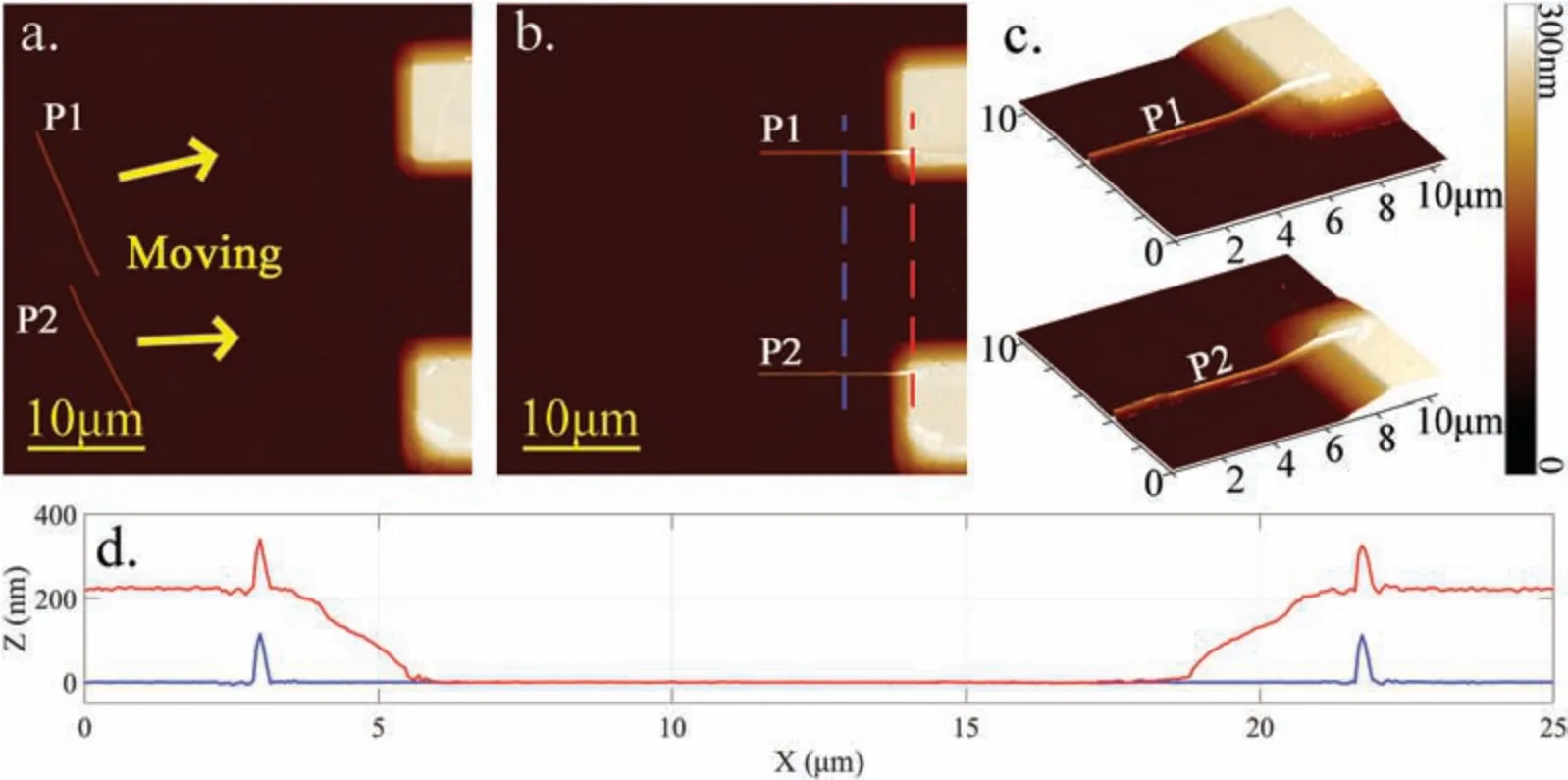
FIG.5.Process of constructing nanoprobes:(a)moving the probe nanowires onto the gold pads by AFM nanomanipulation;(b)the two probe nanowires on the gold pads;(c)close-up 3D views of the electrodes and nanowires;(d)section views of the gold pads and probe nanowires.The red and blue curves show the profile of the respective dashed lines in(b).
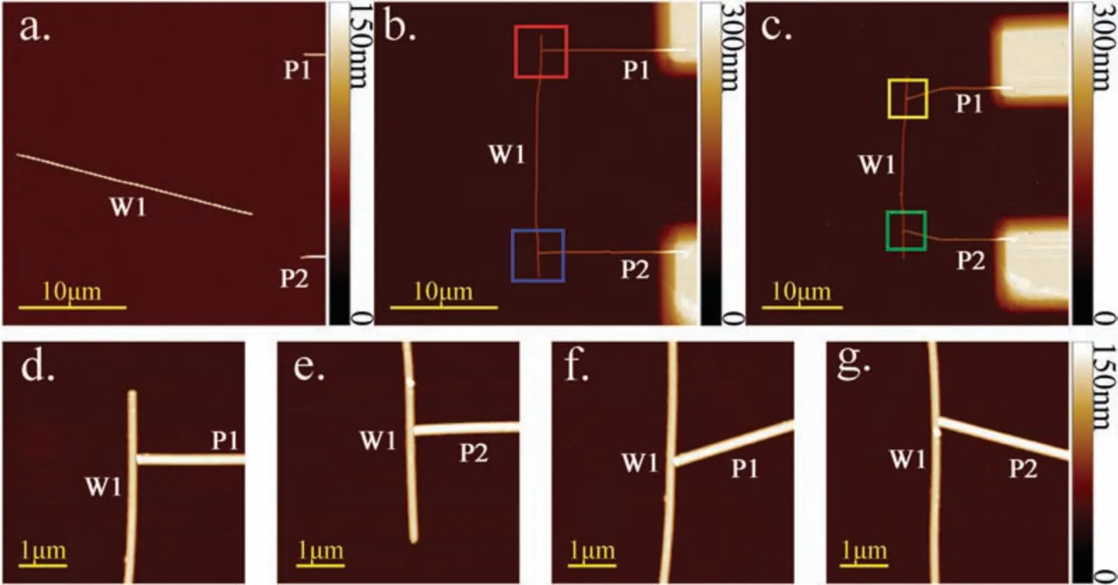
FIG.6.Process of connecting the test nanowire and nanoprobes:(a)a silver nanowire(W1)was moved near the nanoprobes(P1 and P2);(b)W1 was connected with P1 and P2;(c)W1 was connected with P1 and P2 again after bending P1 and P2;(d)and(e)close-ups of the junctions of W1 with P1 and P2 in(b);(f)and(g)close-ups of the junctions of W1 with P1 and P2 in(c).
By changing the distance between the left end points of the nanoprobes,three sets ofIVcurves of the circuit with optimal junctions were measured.In Fig.8(a),the distance is 16.24 μm and the angle of the bent part of the nanoprobes to the horizontal is 15○,so 15○is used to refer to this circuit and itsIVcurve.Similarly,30○and 45○are used to refer to the circuits andIVcurves in Figs.8(b)and 8(c),respectively,where the distance between the endpoints of probe nanowires is 13.97 μm and 9.40 μm,respectively.
IV.RESULTS AND DISCUSSION
For the three sets of data in Fig.8(the 15○,30○,and 45○sets),the backward curves always show better stability than the forward curves.In fact,the forward process can also be considered as a type of electroforming,so the junctions are more optimized during the backward process.Therefore,the backward values were chosen for the calculation.

FIG.7.IV curves of the circuit(a)before and(b)after electroforming.
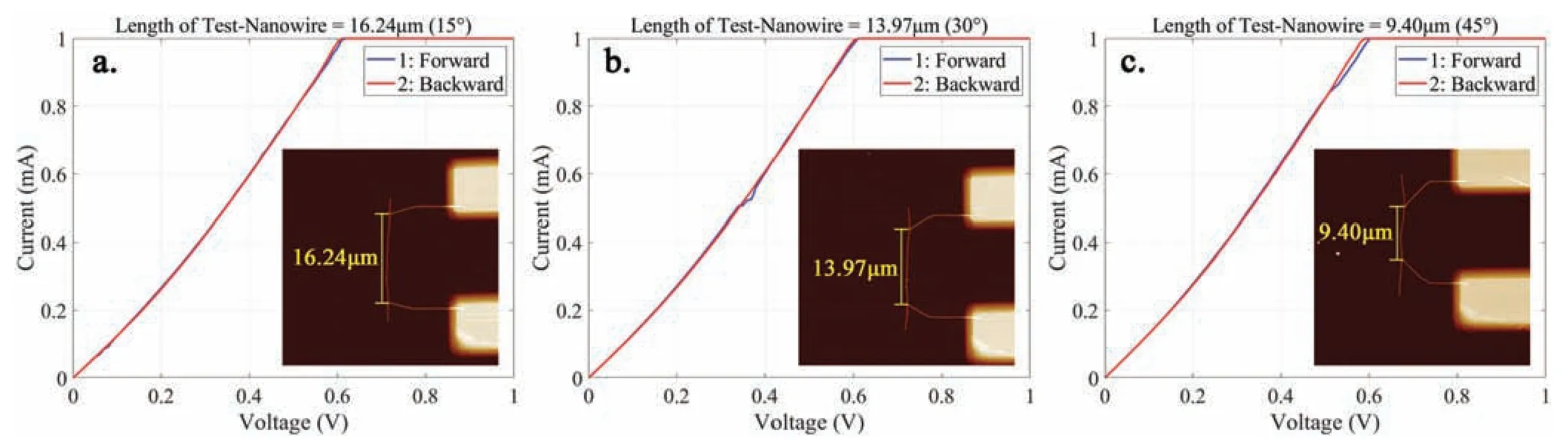
FIG.8.IV curves with different lengths of nanowire after electroforming.The saturation current was set to 1 mA to avoid heat loss in the nanowire caused by a high current.The blue curve corresponds to the voltage increasing from zero to 1 V,while the red curve corresponds to the opposite process.Measurements were made using a test step size of 0.01 V.Nanowire length:(a)16.24 μm(15○);(b)13.97 μm(30○);(c)9.40 μm(45○).
For better comparison,we selected the data in the voltage range of 0.05–0.55 V in the three backward curves for analysis.By dividing the voltage values by the current values,the total resistance of the circuit was obtained as shown in Fig.9(a).The resistance curves show that the total resistance of the circuit did not decrease over time,i.e.,theIVcurves obtained during repeated measurements are highly overlapping (as shown by the forward and backward curves in Fig.8).However,the circuit still had different resistance values at different voltages,as indicated by the nonlinearity of theIVcurves.
Because the measured W1 nanowire for the 45○set was the shortest,its corresponding resistance was the smallest.Therefore,the ΔRcurves in Fig.9(b)were obtained by subtracting the 45○resistance values from the 15○and 30○ones.The blue circles represent the differences in resistance values between the 15○and 45○sets,and the average value is(ΔR15-45)mean=33.13 Ω.The red circles represent the differences in resistance values between the 30○and 45○sets,and the average value is(ΔR30-45)mean=20.32 Ω.
As can be seen,compared with the ΔR30-45curve,the ΔR15-45curve has a more apparent decreasing trend with increasing voltage.A possible reason for this is that the 15○set was the firs set of measurements to be made,and some junctions in the circuit may not have been optimal at that time.Consequently,theIVcurve of the 15○set has a more significan nonlinearity,which means that theR15curve is more inclined compared withR30andR45curves.By contrast,for the 30○and 45○characterizations,the junctions were much closer to optimal and so contributed more similarly during the characterizations.Therefore,it is reasoned that the values of ΔR30-45are more suitable for calculating the resistivity of W1.The standard deviation of ΔR30-45and the resistivity of the silver nanowire are calculated as
where std(X)is a function that returns the standard deviation of the elements ofX,andris the radius of W1,which is 50 nm.
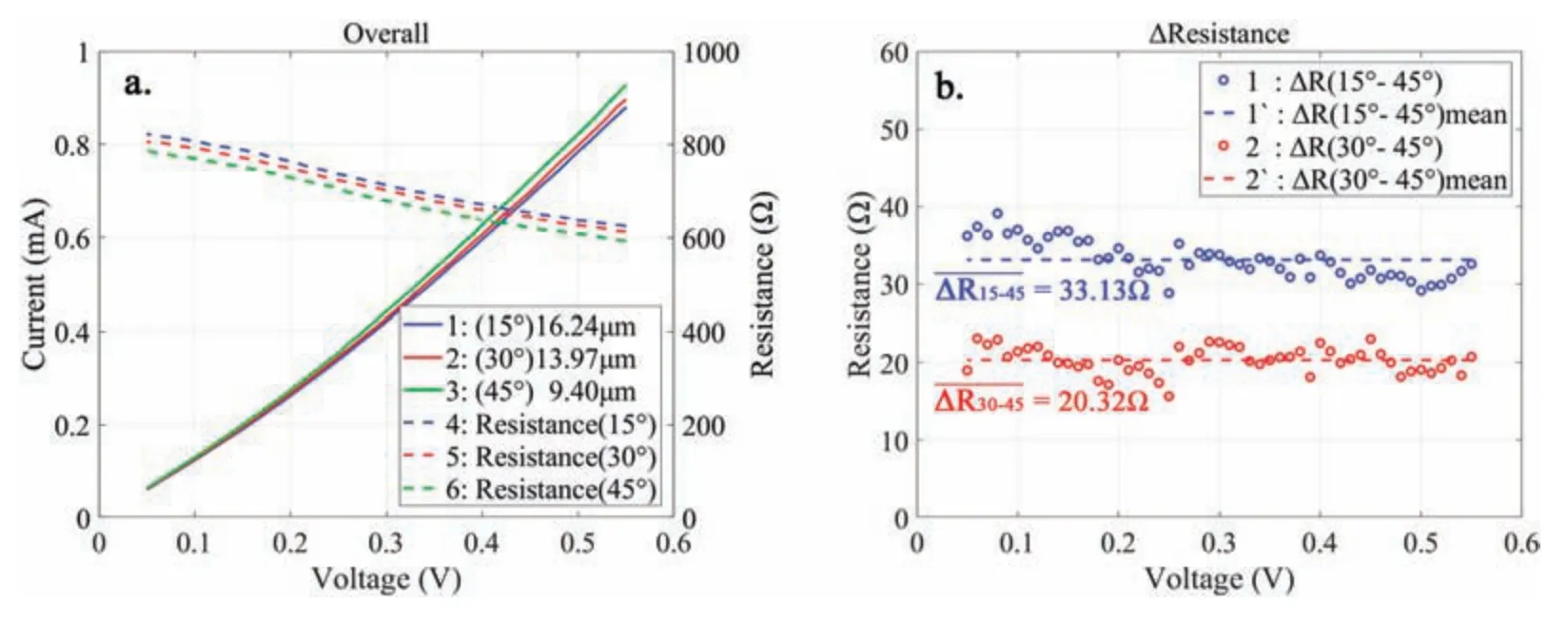
FIG.9.Results for electrical characteristics:(a)IV and resistance curves;(b)ΔR.
The results show that the resistivity of an individual silver nanowire with a diameter of 100 nm is (3.49 ± 0.28) × 10-8Ω m,which aligns well with previous measurements of from 2.03× 10⁻⁸Ω m to 4.60 × 10⁻⁸Ω m.5,25,26,30The reason for the difference in results may be the different ways in which the silver nanowires were produced.Besides,some of the tests were carried out in an SEM,and so the electrons adsorbed on the samples could also have affected the conductivity.Moreover,previous studies have shown that the resistivity of metallic nanowires—including silver ones—tends to increase with decreasing cross section.The commonly accepted reason for this is that surface and grain-boundary scattering contributes to the electrical resistivity of nano-objects whose critical dimensions are more than tens of nanometers.These theories are generally thought to explain the experimentally observed phenomenon of increasing nanowire resistivity with decreasing wire size.25They also explain why the resistivity values for silver nanowires are higher than that of bulk silver,which is 1.62×10⁻⁸Ω m.
V.CONCLUSIONS
Presented herein was a method for characterizing the electrical properties of individual silver nanowires utilizing AFM-based nanomanipulation technology.A pair of flexibl nanoprobes in the form of silver nanowires was fabricated to enable flexibl adjustment of the contact points on the silver nanowire sample.MultipleIVmeasurements were performed to mitigate the influenc of contact resistance across different areas of the sample.Ultimately,the resistivity of an individual silver nanowire with a diameter of 100 nm was determined to be(3.49±0.28)×10-8Ω m.The proposed method can be applied to the measurement of not only silver nanowires but also other 1D materials.Also,because of the high efficienc and accuracy of nanomanipulation in rearranging the positions and orientations of nanowires,this technique holds promise for constructing and modifying diverse prototype circuits based on low-dimensional nanomaterials.
ACKNOWLEDGMENTS
This work was supported by the National Natural Science Foundation of China(Grant No.61973233).
AUTHOR DECLARATIONS
Conflict of Interest
The authors have no conflict to disclose.
Author Contributions
R.Z.and S.W.contributed equally to this work.
DATA AVAILABILITY
The data that support the finding of this study are available from the corresponding authors upon reasonable request.
- 纳米技术与精密工程的其它文章
- Stress distribution variations during nanoindentation failure of hard coatings on silicon substrates
- Electrode design for multimode suppression of aluminum nitride tuning fork resonators
- Effects of simulated zero gravity on adhesion,cell structure,proliferation,and growth behavior,in glioblastoma multiforme
- Design and analysis of longitudinal–flexuralhybrid transducer for ultrasonic peen forming
- An advanced cost-efficient IoT method for stroke rehabilitation using smart gloves
- An image mosaic technique with non-overlapping regions based on microscopic vision in precision assembly