
A low-noise,high-gain,and large-dynamic-range photodetector based on a JFET and a charge amplifier*
2024-03-01 04:06JinrongWANGShuangWUChengdongMIYanerQIUXinaiBAI
Jinrong WANG ,Shuang’e WU ,Chengdong MI ,Yaner QIU ,Xin’ai BAI
1Department of Physics, Lyuliang University, Lvliang 033001, China
2Guangdong Provincial Key Laboratory of Fiber Laser Materials and Applied Techniques, South China University of Technology,Guangzhou 510640, China
Abstract: We demonstrate a low-noise,high-gain,and large-dynamic-range photodetector (PD) based on a junction field-effect transistor (JFET) and a charge amplifier for the measurement of quantum noise in Bell-state detection (BSD).Particular photodiode junction capacitance allows the silicon N-channel JFET 2sk152 to be matched to the noise requirement for charge amplifier A250.The electronic noise of the PD is effectively suppressed and the signal-to-noise ratio (SNR) is up to 15 dB at the analysis frequency of 2.75 MHz for a coherent laser power of 50.08 μW.By combining of the inductor and capacitance,the alternating current (AC) and direct current (DC) branches of the PD can operate linearly in a dynamic range from 25.06 μW to 17.50 mW.The PD can completely meet the requirements of SNR and dynamic range for BSD in quantum optics experiments.
Key words: Quantum noise;Bell-state detection (BSD);Photodetector (PD);Junction field-effect transistor (JFET);Charge amplifier
1 Introduction
The task of precisely detecting the optical noise at the quantum noise limit is ubiquitous across quantum optics experiments,such as continuous variable quantum optical measurement (Breitenbach et al.,1997;Vahlbruch et al.,2016;Shi et al.,2020;Tian L et al.,2021;Lin et al.,2022),quantum key distribution(Wang XB,2018;Pirandola et al.,2020;Lim et al.,2021;Tian Y et al.,2022;Zhang X et al.,2022;Ma et al.,2023),and quantum information (Liu MM et al.,2017;Liu SS et al.,2020;Langenfeld et al.,2021;Yu and Bai,2021;Li XW et al.,2022;Weigang L et al.,2022;Palmer,2023;Shi et al.,2023).It is generally accomplished using the balanced homodyne detection (BHD) or Bell-state detection (BSD) (Yuen and Chan,1983;Zhang J and Peng,2000).Compared with BHD,BSD can acquire signal beam information through a 50/50 splitter without the local oscillator,greatly simplifying the experimental setup (Wang JR et al.,2019).However,the signal beam is rather weak in such applications,typically 50 μW.It is desirable that the measured signal-to-noise ratio (SNR) is limited by the quantum noise presented on the signal beam rather than the electronic noise introduced by the photodetector (PD).Therefore,one challenge,which is the particular focus of this study,is the design and characterization of a PD that can accurately measure the quantum noise of a signal beam at the power level of 50 μW.
One popular approach for suppressing the electronic noise and improving the SNR is to adopt transimpedance-amplification-circuit architecture (Gray et al.,1998;Okubo et al.,2008;Kumar et al.,2012;Jin et al.,2015;Qin et al.,2016;Masalov et al.,2017;Bowden et al.,2019),in which the special considerations in a high-frequency range are the input-voltage noise of the operational amplifier (OA) and the total input capacitance (Yang X et al.,2019),including the junction capacitance of the photodiode,the input capacitance of the OA,and the parasitic capacitance of the developed printed-circuit board (PCB).As such,Zhou et al.(2014) suppressed the electronic noise by reducing the junction capacitance of the photodiode based on the bootstrap structure,where the SNR reached 13 dB at an analysis frequency of 2 MHz for a 50-μW laser.Subsequently,by adopting a junction field-effect transistor (JFET) buffering input on the basis of the bootstrap structure,the SNR at 2 MHz was 0.5 dB smaller,but it increased from 6.0 to 9.8 dB at 4 MHz(Zhou et al.,2015).Appel et al.(2007) showed an explicit relationship between the SNR and equivalent optical efficiency.A PD with a high SNR is urgently needed to enable the accurate detection of high-level squeezed light in a high-frequency range.In the case of squeezed light of 15 dB with power of 50 μW,the measurable squeezing level was only 10.96 dB for a PD with an SNR of 13 dB (Wang JR et al.,2020).
In this study,we have developed a low-noise,high-gain,and large-dynamic-range PD based on a JFET and a charge amplifier.By suppressing the input-voltage noise based on a JFET and a charge amplifier and reducing the total input capacitance using a photodiode with low junction capacitance,the electronic noise of the alternating current (AC) branch is significantly decreased.Simultaneously,the direct current (DC)branch provides a monitoring signal for laser beam alignment.As a result,when the laser power is about 50.08 μW,the maximum SNR of the AC branch reaches 15 dB in the range of 2–5 MHz.In addition,the AC and DC branches show excellent linearities in the dynamic range from 25.06 μW to 17.50 mW.It is extremely appropriate for weak optical signal detection,which will facilitate quantum optics experiments as well as relevant research.
2 Photodetector design
2.1 Design principles
The optical noise at the quantum noise limit,also called quantum noise,is the main and the most significant noise in an optical system;it is at the lower bound of the classical noise.As we know,optical losses and phase fluctuations can reduce the level of squeezing;the quantum efficiency of a photodiode and the SNR of a PD further deteriorate the level of measured squeezing.The transimpedance amplifier (TIA) provides the most successful approach for providing high SNR in a high-frequency regime (Graeme,1995;Bickman and DeMille,2005).A typical transimpedancebased PD circuit and the equivalent circuit with noise sources are given in Fig.1.The bias voltageVoof the photodiode reduces the inherent junction capacitance to increase the amplification bandwidth.The feedback capacitanceCfis used to prevent self-induced oscillation by compensating for the transfer phase delay.The electronic noise of the TIA,obtained in the absence of an input-laser beam,originates from the feedback resistanceRfand the OA.The thermal noise ofRfis the Nyquist noise.The noise contribution of the OAis modeled by current and voltage supplies with the values ofinoiandenoi,respectively.The noise associated with the dark currentIdkand the shunt resistanceRdof the photodiode is negligibly small.According to Masalov et al.(2017),we shall calculate the noise contributions of each noise source separately and combine their squared values.
The noise contribution produced by the thermal noiseof the feedback resistanceRfis given by
whereG(f) is the OA gain,Kis Boltzmann’s constant,Tis the absolute temperature,and Δfis the unity measured bandwidth.
The noise contribution of the OA current noiseinoican be expressed as
The noise contribution of the OA voltage noiseenoiat a given frequencyfhas the form
wherefis the analysis frequency,andCdandCinare the inherent capacitances of the photodiode and the OA,respectively.
Since all of the electronic noise terms mentioned above are uncorrelated,the total electronic noise can be deduced as
We can see that the noise contributions generated byRfandinoiare white,while the noise contribution ofenoiis linearly related to the square of the frequency.This is because the OA voltage noise,imposed on the capacitive impedance,gives rise to the current noise that is proportional to the frequency.Hence,the noise contribution of the voltage noise is dominant for the low electronic noise and good SNR in the high-frequency domain,which demands attention to both photodiode and OA selection and the PCB layout.The choice of photodiode is effortless for high quantum efficiency and small junction capacitance.Additionally,the PCB layout is designed on the basis of the high-frequency PCB design principle(Kumar et al.,2012).Careful positioning of the photodiode and OA can minimize the stray capacitance.Conventionally,an OA with ultra-low input-voltage noise,small input capacitance,and large gain bandwidth product (GBP) is preferred for TIAs with a high SNR in a high-frequency regime.However,there is a contradiction between the input-voltage noise and GBP;how to carry out a compromise design is a key aspect of the technology in the PD design process.An alternative approach is the combination of a JFET and an OA,where the JFET is followed by the OA.Since the JFET input stage does not have enough gain to achieve the desired transimpedance gain,it can provide a lower noise amplification stage so that the inputvoltage noise of the OA is negligible;meanwhile,the GBP remains unchanged (Bickman and DeMille,2005;Huang et al.,2013;Zhou et al.,2014;Bowden et al.,2019).
2.2 Implementation
According to the theoretical analysis,a schematic of the PD is given in Fig.2.To reduce loss and obtain the maximum possible SNR,a specially made InGaAs-PIN photodiode (from Laser Components,Germany) is selected with more than 99% quantum efficiency at 1064 nm and 1.0 pF of junction capacitance (Yang WH et al.,2017).Inductor L1 and capacitance C1 are combined to separate the shot noise current (AC current) and mean photocurrent (DC current),which characterize the vacuum fluctuation and optical power of the measured laser,respectively.

Fig.2 Circuit diagram of the photodetector (Filtering and bypassing of power supply are performed in advance)
The choice of a TIA is critical to realizing a good SNR and a large dynamic range.Here we use a charge amplifier A250 for the TIA.A250 is a hybrid state-ofthe-art charge-sensitive amplifier for use with a wide range of detectors with capacitance from <1 pF to several thousand picofarads,such as photomultiplier tubes,piezoelectric devices,and photodiodes.Such applications allow the field-effect transistor (FET) to be matched to the particular detector capacitance as well as to the noise requirement.The noise performance of A250 is such that its contribution to FET and detector noise is negligible.Note that A250 is used not only as a charge amplifier but also as a high-performance voltage amplifier by choosing a resistance as the feedback component.Based on the used photodiode junction capacitance and A250 noise characteristics,the silicon N-channel JFET 2sk152 is a perfect option for low electronic noise.In addition,capacitances C2 and C4 are added to further suppress the electronic noise.To obtain the highest SNR,we combine a feedback resistance R5 of 200 kΩ and a compensation capacitance C5 of 0.5 pF,which prevents selfoscillation by compensating for the transfer phase delay.
In the DC amplification branch,the OP27 precision OA with low offset and noise allows accurate highgain amplification of DC and low-frequency signals.The voltage generated across resistance R4 by the DC photocurrent is amplified without self-oscillation for laser alignment.The adjustment of DC voltage gain by P1 is necessary to make the AC and DC branches have the same saturated optical power.
The PCB layout for the circuit diagram shown in Fig.3 is the last step,but it is quite critical throughout the design process.Wang SF et al.(2017) verified that the stray capacitance on the developed PCB has a non-negligible influence on the PD’s performances by establishing a theoretical simulation model.Hence,it needs to be seriously considered to reduce the unwanted stray capacitance and inductance.First,the tracks on the PCB are kept as short as possible to reduce the stay inductance.Second,a ground plane with the fewest possible discontinuities is designed on the back side of the PCB,which can minimize the stray capacitance between the tracks and the ground plane.Finally,the PCB is shielded by a machined metal box to prevent any external electromagnetic noise on the PD circuit.
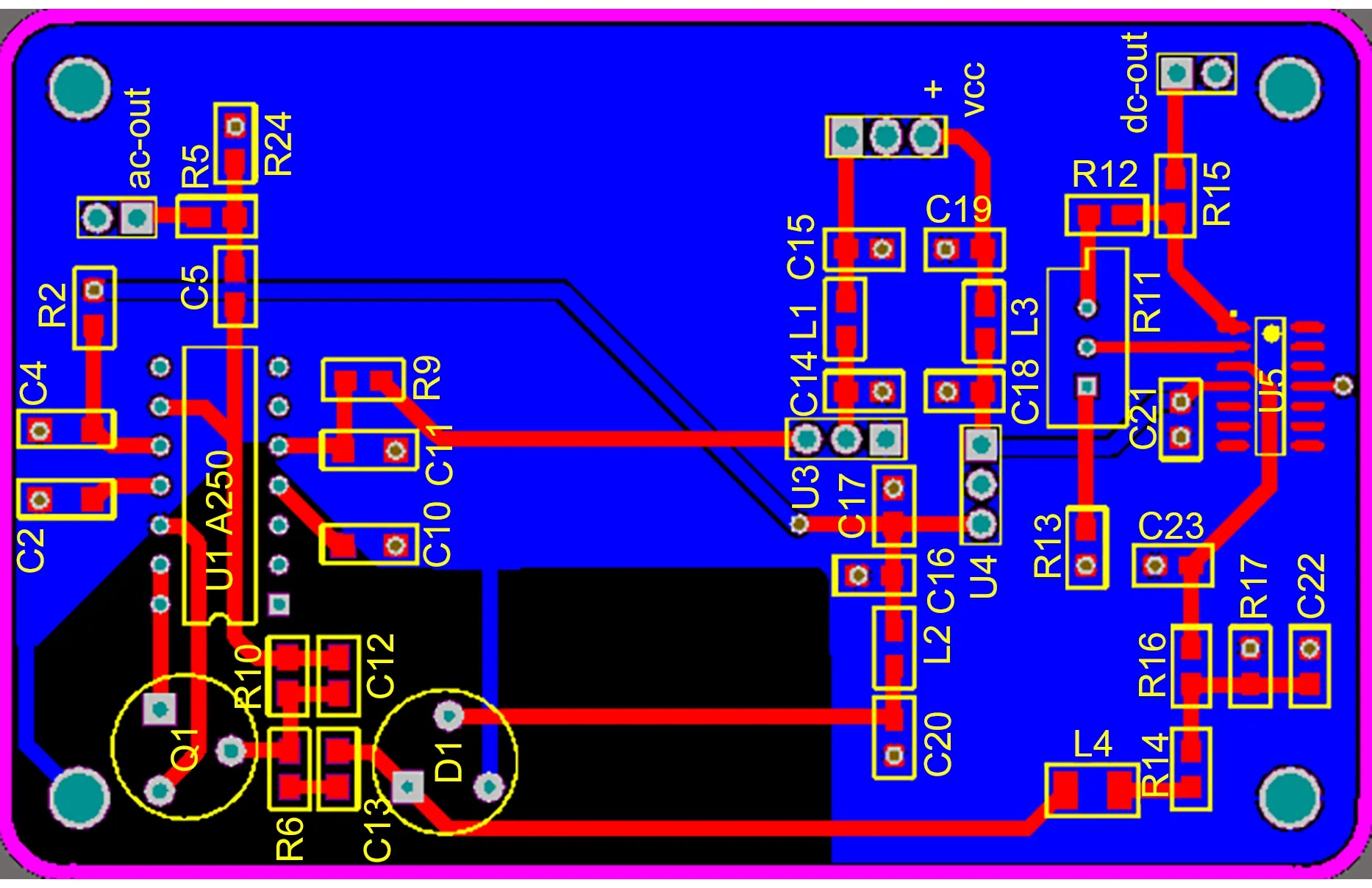
Fig.3 Printed-circuit board layout of the photodetector
3 Experimental results and analysis
We designed and built the high-performance PD with a focus on measuring the level of squeezing and entanglement on a large scale at high frequencies.The experimental setup was constructed to evaluate the performance of the PD,as shown in Fig.4.
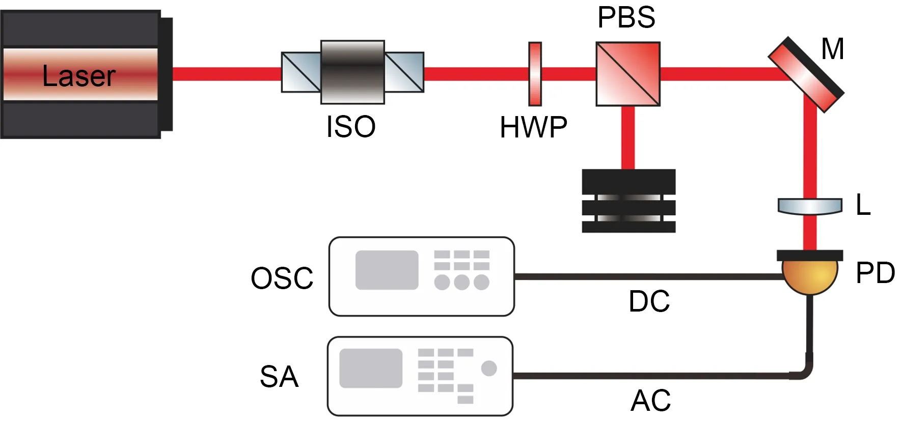
Fig.4 Experimental setup for measuring the performance of the photodetector
The laser source was a single-frequency Nd:YVO4laser at 1064 nm with the maximum output power of 300 mW;its output power can be conveniently adjusted by a power adjustment system consisting of a halfwave plate (HWP) and a polarization beam splitter(PBS).An optical isolator (ISO) in front of the laser was used to minimize the back reflections.The output beam of the PBS was injected into the PD after being focused with the focusing lens L.The DC output of PD was connected with a digitizing oscilloscope (OSC)to verify whether the laser was thoroughly received by the photodiode while providing a monitoring signal for the input-laser power measurement.The AC output was connected with a spectrum analyzer N9010A to read the noise power.
First,the noise power of the AC branch and the corresponding DC voltage of the DC branch were simultaneously achieved at several incident powers.As shown in Fig.5a,the noise power increased with the increasing incident power.However,when the incident power exceeded the PD saturation power of 17.50 mW,the noise-power curve dropped rapidly due to the OA saturation.In particular,the maximum SNR reached 15 dB in the range from 2 to 5 MHz for the incident laser power of 50.08 μW.Additionally,as shown in Fig.5b,the noise power and the DC voltage were fitted based on the experimental data in Fig.5a.Theoretically,when the incident laser was at the shot noise limit,the shot noise power showed a 3-dB difference with the double variation of the incident laser power.The noise power of the AC branch in Fig.5b entailed a 3-dB shift of the corresponding noise trace in the range from 2 to 5 MHz when changing the laser power from 25.06 μW to 12.81 mW by a factor of two,which was in agreement with the theoretical result.It indicated that the incident laser was at the shot noise limit at 2 MHz and the AC branch operated linearly in the analysis frequency regime,which are essential for accurately measuring the level of squeezing and entanglement.Furthermore,the DC branch showed good linear correlation,so the input laser power can be conveniently read without the power meter.Note that even though the scales of the input laser power and the DC voltage in Fig.5b were replaced with a logarithmic scale,they had no influence on the demonstration of the excellent linearities of the AC and DC branches.

Fig.5 Noise power of the AC branch measured by the spectrum analyzer at several incident powers (a),and linearities of the AC and DC branches fitted from 25.06 μW to 17.50 mW (b)
To investigate the dependence of the measured squeezing factorSon the SNR of the AC branch,for the SNR of the AC branch at 2.75 MHz and the measured squeezing factorSfor squeezed light of 15 dB in an incident laser power range of 25.06 μW–17.50 mW,we haveS=|10[(1-10-0.1SNR)×10-1.5+1 0-0.1SNR]|.Here,the escape efficiency of the optical parametric amplifier,the reflectivity of the reflecting mirror,and the quantum efficiency of the photodiode were assumed to be 100%.As Fig.6 shows,the SNR of the AC branch and the measured squeezing factor increased linearly and exponentially with the increasing input laser power,respectively.Obviously,the measured error of the squeezing factor decreased gradually with the doubling of the laser power.This is because,compared with the measured squeezing factor for the mW-scale laser power,the measured squeezing factor for the μW-scale laser power was strongly dependent on the SNR of the AC branch.Generally,the power of squeezed light was only tens of microwatts for the consideration of the high squeezing factor in the preparation of squeezed light.Thus,the PD with a high SNR in the μW-scale laser power can more accurately measure the squeezed light.In the case of squeezed light of 15 dB with the power of 50.08 μW,the measured squeezing factor rised from 10.96 to 12.06 dB when the SNR of the AC branch increased from 13 to 15 dB.

Fig.6 Signal-to-noise ratio (SNR) of the AC branch for the laser power from 25.06 μW to 17.50 mW and the corresponding measured squeezing factor for squeezed light of 15 dB obtained at 2.75 MHz
4 Conclusions
In conclusion,we have developed a low-noise,high-gain,and large-dynamic-range PD based on a JFET and a charge amplifier for the measurement of quantum noise in BSD.Based on the junction capacitance of 1 pF for a specially made InGaAs-PIN photodiode from Laser Components,the silicon N-channel JFET 2sk152 is preferred for satisfying the noise requirement for charge amplifier A250,and the electronic noise is effectively suppressed.By adopting the combination of an inductor and a capacitance,the AC and DC branches of the PD can operate independently and linearly in a dynamic range of 25.06 μW–17.50 mW.The maximum SNR reaches 15 dB in the range of 2–5 MHz for a coherent laser power of 50.08 μW.In addition,the DC branch provides a monitoring signal for laser beam alignment.The PD can completely meet the requirement of weak optical signal detection,quantum optics experiments,and relevant research.
Contributors
Jinrong WANG designed the research.Chengdong MI processed the data.Shuang’e WU drafted the paper.Yaner QIU helped organize the paper.Jinrong WANG and Xin’ai BAI revised and finalized the paper.
Compliance with ethics guidelines
Jinrong WANG,Shuang’e WU,Chengdong MI,Yaner QIU,and Xin’ai BAI declare that they have no conflict of interest.
Data availability
The data that support the findings of this study are available from the corresponding author upon reasonable request.
 Frontiers of Information Technology & Electronic Engineering2024年2期
- Frontiers of Information Technology & Electronic Engineering的其它文章
- Towards resilient average consensus in multi-agent systems:a detection and compensation approach∗&#
- Modified dynamic event-triggered scaled formation control for multi-agent systems via a sparrow search algorithm based co-design algorithm∗
- Event-triggered distributed optimization for model-free multi-agent systems∗#
- Event-triggered finite-time command-filtered tracking control for nonlinear time-delay cyber physical systems against cyber attacks∗
- Outlier-resistant distributed fusion filtering for nonlinear discrete-time singular systems under a dynamic event-triggered scheme∗
- Recursive filtering of multi-rate cyber-physical systems with unknown inputs under adaptive event-triggered mechanisms∗#