
Effects of Three-dimensional Ehrlich-Schwoebel Barriers on Cu(111) and Cu(100) Homoepitaxial Growth
2017-06-21 10:48DONGGuirenTANGJiyuCUIJingLIUJuanHEYouqing
材料科学与工程学报 2017年3期
DONG Guiren, TANG Jiyu, CUI Jing, LIU Juan, HE Youqing
(Department of Physics and Telecommunication Engineering, South China Normal University, Guangzhou 510006, China)
Effects of Three-dimensional Ehrlich-Schwoebel Barriers on Cu(111) and Cu(100) Homoepitaxial Growth
DONG Guiren, TANG Jiyu, CUI Jing, LIU Juan, HE Youqing
(Department of Physics and Telecommunication Engineering, South China Normal University, Guangzhou 510006, China)
The 3-dimensional Ehrlich-Schwoebel(3D ES) barriers directly affect the interlayer diffusion, and the 2D ES barrier and the 3D ES barrier are different on the Cu(111) and Cu(100) surface respectively. Based on (1+1) dimensional KMC method, we mainly focused on the homogeneous epitaxial growth of Cu films on these two special crystal surfaces in this paper. And we found that the roughness of the film decreases with the increase of temperature. The roughness on Cu(111) surface drops faster than that on Cu(100) surface, and Cu(111) surface is more conducive to the growth of film due to lower 2D ES barrier. For the application of nanorods, the growth rate declines gradually when the growth time is short, but the growth rate of Cu(100) surface is faster than that on Cu(111) surface. However, with the growth time increasing, the effects on these two surfaces are different in appearance of multi-layer steps. The growth rate of Cu(111) surface rises and eventually exceeds the Cu(100) surface. The multi-layer steps formed on Cu(111) surface is more favorable for the growth of nanorods because of the larger 3D ES barrier while the multi-layer steps are hard to form on Cu(100) surface and the growth rate of nanorods does not increase due to the lower 3D ES barrier. The existence of 3D ES barrier leads to the emergence of multi-layer steps and the larger 3D ES barrier is conducive to the growth of nanorods.
Kinetic Monte Carlo simulations; surface roughness; thin film growth; (1+1) dimensional
1 Introduction
Computational nanostructure simulations (such as nanodot, nanowire and thin film) have always been popular. With decants of theoretical and experimental researches, reliable methodology has been established, which enables individuals to have an insightful understanding of nanostructure formation mechanism[1-5]. Currently, film computational simulation methods include molecular dynamics method (MD), Monte Carlo method (MC) and Kinetic Monte Carlo method (KMC), etc. Among these computational methods, the KMC method is a powerful material modeling tool in long time scale[6]. R.Zhang[7]and S.Ruan[8]employed KMC method based on (1+1) dimensional to simulate the film growth. R.Zhang found that a larger 3D ES barrier led to higher stability and more multi-layer steps. But he only studied the Cu(111) surface, and he didn’t consider Cu(100) surface.
Flat diffusions of adatoms have been exhaustively studied[9-12]and the interlayer ones have also received great attention[13]. In 1966, Ehrlich, Schwoebel and his co-workers studied adatom interlayer transmission. They found that an additional barrier should be overcome for an adatom to migrate down the surface step[14-15]. The additional barrier is called Ehrlich-Schwoebel (ES) barrier or 2D ES barrier. A variety of computer simulations have been adopted to study the effects of ES barrier, which controls mass adatoms transport during surface deposition and has impact on thin film roughness[14-18].
Additional studies generalized the conventional concept with 3D ES barriers, which refer to the barrier needs to be conquered when adatom effectively diffuses down a multiple layer step[19]. Considerable researchers[7,20]pointed out that substantial differences exist between 2D and 3D barriers. Molecular Dynamics and Molecular Statics methods were employed to explicit the exact value of some specific materials, based on a broad area of research fields. In the study of R. Zhang et al[7], it has found that the 3D-ES barriers stabilize multi-layer steps. The stability was improved due to the presence of 3D-ES barrier which was larger than 2D ES barrier in that specific condition. However, according to the study of S. J. Liu et al[19], there is a major disparity in the 3D barriers between two facets. Sun Jie et al, prepared Cu2O thin films by experiment and studied the optical properties of them. Liang Jingshu et al, using Monte Carlo model investigated the effects of Si(100) pre structure substrate on the growth of three dimensional simulation of Si sculptured thin film. Zhu Chunzhang simulated the effects of grain boundaries on the hole expansion in nanocrystalline copper via the molecular dynamics model.
The effects of 3D-ES barriers on Cu(100) surface and Cu(111) surface of thin film growth have been studied, but the analysis is rare for 3D-ES barrier on Cu (100) and Cu (111) surface of nanorod growth. Based on H. Huang’s work[21]and (1+1) dimensional Kinetic Monte Carlo (KMC) model, this paper has studied the effects of 3D-ES barrier on Cu (100) surface and Cu (111) surface of thin films and nanorods homoepitaxial growth. According to the results, multiple-layer steps in mode surface Cu(111) benefit the growth of nanorods. This mechanism does not exist on surface Cu(100) and its growth rate decreases. The large 3D-ES barrier benefits the growth of nanorods. In addition, Cu (100) surface is suitable for the growth of nanorods while Cu (111) surface is suitable for the growth of thin films.
2 Modeling
Kinetic Monte Carlo (KMC) method based on (1+1) dimensional is employed. Atoms are deposited a
t a fixed rate on the surface of substrate which is initial flat with constant temperature and periodic boundary conditions. The particles move in the following situations in the process of the thin film growth : (1) deposition: vapor particles incident on the surface and adsorption become adsorbed species on the surface; (2) diffusion: adsorbed particles jump to another position form one position on the surface; (3) reevaporation: adsorption energy particles from the substrate will be large enough for desorption. The rates of these three processes correspond to the deposition rate, the diffusion rate and desorption rate, respectively.
Deposition process is determined by deposition rate. The deposition rate Vdgiven by Vd=FN where N is the sum of positions on the substrate and F is the deposition rate given in monolayers per second (ML/S).
The reevaporation process is determined by the reevaporation rate Vr given by
(1)

If the particles is absorbed on the substrate, the particles may stop moving or diffusing on the substrate. Deposition particles diffusion on the substrate is the key of the thin film growth, the adsorption particles diffusion on the substrate can be divided into the following forms: (1) the particle deposition to the substrate, (2) the adsorption particles diffuse on the substrate surface, (3) diffusion particles with another particle form nuclear, (4) the diffusion particles was captured by the existing island, (5) the adsorption particle deposition on the island of existing and conduct flat diffusion or interlayer diffusion. (6) deposition particles have low energy or the diffusion positions around the particles are occupied by another particle to stop movement. Figure 1 shows several cases of diffusion movement on the substrate surface: a) gas phase particle deposition, b) adsorption particles diffusion on the flat, c) adsorption particle diffusion on the mono-layer. d) adsorption particle diffusion on the multi-layer.
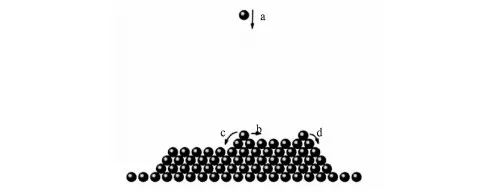
Fig.1 A schematic of growth process in our simulation, consisting four different kinds of events: a) deposition, b) flat diffusion, c) mono-layer diffusion and d) multiple-layer diffusion
Diffusion rate to potential sites determine their hop probabilities.
(2)

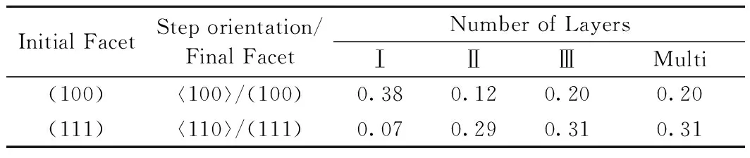
Table 1 ES barrier (eV) as a function of number of layers of each step
Deposition, diffusion and reevaporationcan be selected by using rate Vh, Vd, Vr. If reevaporation happens, a surface atom is removed to form the substrate randomly. However, due to a large energy to be overcome for reevaporation of the particles, the probability of partical reevaportion is very low. In this paper, the reevaportion process is not considered. If deposition event is selected, the atom is deposited on the substrate randomly. If diffusion takes place, the atom will diffuse from one site to another, and the diffusion direction is determined by a random number R, R is between 0 and 1,
If the event n satisfies the formula (1), the event n will happen
(3)
The full expression of the time increment isΔt,given by
(4)
In this paper, software C# language was used, with Microsoft Visual Studio 2010 as a platform for simulation, the simulation processes are as follows:
(1)To set the periodic boundary conditions, substrate size, temperature, and other parameters.
(2)To randomly generate a coordinate, if no particles in this coordinate below Z, so z become Z-1, until the deposited particles fall into the substrate. Reproject a new deposition atom on the substrate if this coordinate is higher than the present coordinate.
(3)Analyzing diffusion particles may have a hop sites around the position, if all of sites is occupied by other particles, execution (5), otherwise execution (4);
(4)The diffusion is selected, execution (6);
(5)The deposition is selected;
(6)Refresh the position of deposition particles and calculate the simulation time, if the simulation time is less than a preset time to execute (3);
(7)Terminate the program and output data to analysis.
3 Results & Discussions
In the simulation, deposition rate is a constant and temperature ranging from 200K to 700K is fixed in each running. The possibility of particles randomly depositing each position is equal and deposition position from 0 to 200, 2000 atoms were deposited. Fig.2 shows film morphology on Cu (100) surface in condition of changing temperature. The evolution trend shows that the higher the temperature is, the smoother the film will be, which can verify our simulation mode.
From the values listed in Table 1, it can be inferred that growth situation is distinctly different on surface Cu(100) from Cu(111). 2D ES barrier of Cu(100) is much larger than that of Cu(111) while it Cu(100) becomes smaller when it comes to 3D ES barrier. The prediction of growth situation on the two surfaces is hard. Therefore, the following tests are settled.

Fig.2 Morphology evolution of thin film on surface Cu(100) when the temperature ascends from 200K to 700K, F=0.1ML/S
3.1 Thin film
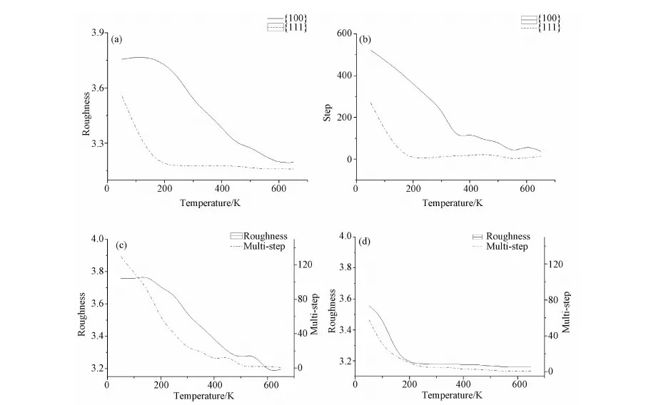
Fig.3 Image a) shows surface roughness as a function of temperature; Image b) shows step as a function of temperature; Image c) and d) respectively present the roughness and multiple-step variations with temperature on surface Cu(100) and on surface Cu(111), F=0.1ML/S
before 200K and changes little since then. From the comparison, the growth on Cu(111) surface unequivocally smoother than that on Cu(100) in conditions of equivalent temperature and deposition rate.
Variation of the number of steps is presented in Fig.3b) which resembles that of roughness, indicating less number of steps in high temperature. But step decline faster on the Cu(111) surface than that on the Cu(100). Step decreased rapidly from 0 to 200K on the Cu(111). Fig.3c), 3d) illustrates the relationship of roughness and multiple-steps in Cu(100) and Cu(111) respectively. The changed trends of roughness and multiple-steps are very similar. The vanishing of multiple-step leads to the approximate constant roughness.
3.2 Nnaorods
Based on the work of R. Zhang[7], multiple steps benefit the growth of nanorod while detrimental to that of thin film. From Fig.3c) and 3d), we can see the number of multiple steps is larger in Cu (100) than Cu(111) in the same temperature. Therefore, it can be inducted that for nanorods growth, surface Cu(100) is desirable. Due to the equity deposition probability in each site, deposition of atoms acts as compensation of the interlayer diffusion. To further test the inference above, scenarios of concentrated deposition are settled. Atoms are equally deposited in ranges from site 151 to 250 of the periodic substrate of 400, which could better reflect the growth situation of nanorods. 4000 atoms were deposited. Fig.4 reveals the evolution of nanorods on surface Cu(100) and Cu(111). In general, it is not conducive to growth for nanorods when the temperature rises.
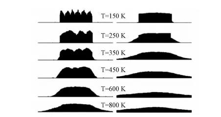
Fig.4 Nanorods evolution via temperature on surface Cu(100) and Cu(111), F=0.1ML/S
Comparing the growth on surface Cu(100) and Cu(111), substantial disparity in variation via temperature is presented. Lateral sides of nanorods on surface Cu(100) appear slow descending with the increase of temperature. However, on surface Cu(111), we can see several steps or multiple-steps. And with the disappearance of multiple-step, the nanorods corrupted. Based on the observation above, it comes to preliminary conclusions: (i) surfaces of Cu(100) are more conductive to the growth of nanorods compared with its equal temperature counterparts on surface Cu(111); (ii) the multiple-steps can facilitate nanorods growth on surface (111); (iii) on surface Cu(100), multiple-steps are not as stable as that of surface Cu(111) and a step-meandering instability phenomenon can be observed.
Further analysis is executed to verify the first inference. Here we introduce concepts of width and altitude of nanorods. Width is defined as the range of X sites which possess more than three atoms. And altitude is defined as the average of all the peaks. Fig.5a), b) shows the variation width and altitude when temperature ascends respectively. It can be figured out in Fig.5c) that the ratio of altitude to width descends with the ascending of temperature and the decrease of surface Cu(111) is faster than its counterpart on surface Cu(100). Accordingly, the surface of Cu(100) is more conducive to the growth of nanorods than on surface Cu(111).
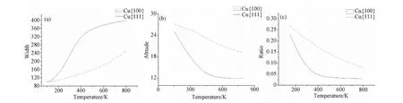
Fig.5 a) Width as a function of temperature; b) altitude as a function of temperature; c) ratio of altitude to width as a function of temperature, F=0.1ML/S
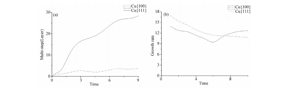
Fig.6 a) the highest layer step evolution with growth process; b) growth rate (differential of height to time) as a function of time F=2.5ML/S, time from 0 to 10.
To testify inferences ii and iii above, growth process with the extension of time at a specific temperature should be scrutinized. We focus on the temperature of 200K for surface Cu(111) and 350K for surface Cu(100) due to their proper atom migration (ratio of altitude to width is approximate 0.2). Growth time varies from one to ten normalized time scale. The lateral sides beyond deposition range are analyzed to elaborate the step changes.
Fig.6a) reveals the dramatic ascending of highest multi-layer steps on the surface Cu(111) and nearly fixed that on the surface Cu(100), which validates the stability mechanism presented by R. Zhangetal[7]. The stability mechanism is that a larger 3D ES barrier leads to higher stability and a larger number of multi-layer steps. Noting that 3D ES barrier less than 2D ES barrier in situation of (100), multiple-steps corrupt easily. Therefore, the growth rate decreased gradually on the surface Cu(100). As a result, the stability mechanism does not exist on the Cu(100) surface. Comparing the growth rate in two surface, it is larger on the surface Cu(100) than Cu(111) initially for its higher 2D ES barrier which blocks the interlayer diffusions. Ascribing to the stability mechanism, growth rate of nanorod on Cu(111) increases while that on Cu(100) decreases, as is showed in Fig.6b), and finally surpasses that on the surface Cu(100).
As is revealed in Fig.7a), growth rate declines initially while the declining tendency ceases after the appearance of multiple-steps. It accelerates the growth rate as well as strengthens the stability of nanorod. As a comparison, Fig.7b) exposes step layer and growth rate on surface (100), pointing out that the scanty of sturdy multiple-steps leads the consistent debilitation of growth rate.

Fig.7 a) the highest layer step and growth rate evolutions with growth process on Cu(111); b) growth rate and highest multiple step layer as a function of time on Cu(100) 4 Summar
We employed a full diffusion Kinetic Monte Carlo (KMC) method based on (1+1) dimensional to simulate effect of three-dimensional Ehrlich-Schwoebel barriers on Cu(111) and Cu(100) homoepitaxial growth modes. We found that the growth process on surface Cu(100) is distinctly different from that on surface Cu(111) due to the substantial disparity of ES barrier. For thin film application, surface Cu(111) is desirable because of the relatively small 2D ES barrier benefiting the migration of adatoms. For nanorods’ applications, the growth time is shorter and the deposition atoms are relatively few. The 2D ES barrier plays a leading role and the growth rate on Cu(100) is faster than that on Cu(111) surface due to larger 2D ES barrier on Cu(100) surface. With the increase of growth time the appearance of multi-layer steps, 3D ES barrier dominates in two surfaces. And the Cu(111) growth rate grows and ultimately exceeds the Cu(100) surface because of the larger 3D ES barrier. Thus, the multi-layer steps on Cu(111) surface are conducive to the growth of nanorods. In addition, the effects of multi-layer on these two surfaces are different. Cu(100) surface is hard to form a multi-layer steps and also makes little contribution to the growth rate of nanorods. From the analysis above, it can be figured out that the multiple-step on surface Cu(111) growth blocks the interlayer diffusion and facilitates the nanorod evolution, while the multiple-steps on (100) acts without the same function.
Reference
[1] A. Chatterjee, D. G. Vlachos. An Overview of Spatial Microscopic and Accelerated Kinetic Monte Carlo Methods[J]. Computer-Aided Materials Design, 2007, 14:253.
[2] A. E. Lita, J. E. Sanchez, Jr. Characterization of Surface Structure in Sputtered Al Films: Correlation to Microstructure Evolution[J].Appl. Phys., 1998, 85:876.
[3] P. B. Barna, M. Adamik. Fundamental Structure forming Phenomena of Polycrystalline Films and the Structure zone models[J].Thin Solid Films, 1998, 317(1):27.
[4] H. Huang, G. H. Gilmer. An atomistic Simulator for Thin Film Deposition in three Dimensions[J].Appl. Phys., 1998, 84: 3636.
[5] M. Kotrla, P. Smilauer.Nonuniversality in Models of Epitaxial Growth[J].Phys. Rev. B., 1996, 53: 13777.
[6] A.Chatterjee, A. F. Voter.Accurate Acceleration of Kinetic Monte Carlo Simulations through the Modification of Rate Constants[J].Chem. Phys.,2010, 132(19): 4101.
[7] R. Zhang, H. Huang. Another Kinetic Mechanism of Stabilizing Multiple-layer Surface Steps[J]. Appl. Phys. Lett., 2011, 98(22): 1903.
[8] S. Ruan, C. A. Schuh. Kinetic Monte Carlo Simulations of Nanocrystalline Film Deposition[J]. Appl. Phys., 2010, 107(7): 3512.
[9] M.I. Rojas, M.C. Gimenez, E.P.M. Leiva.Kinetic Monte Carlo Simulation of Pt Discontinuous thin Film Formation Adsorbed on Au[J]. Surf. Sci., 2005, 581(1): 109.
[10] K. A. Fichthorn, W. H. Weinberg. Theoretical Foundations of Dynamical Monte Carlo Simulations[J]. Chem. Phys., 1991, 95: 1090.
[11] J. M. Rogowska, M. Maciejewski.Kinetic Monte Carlo Study of Fractal Growth with Edge Diffusion and Reversible Aggregation on a bcc(1 1 0) surface[J].Vacuum, 2001, 63: 91.
[12] R. Q. Hwang, J. Schroder, C. Gunther et al. Fractal Growth of Two-dimensional Islands: Au on Ru(0001) [J].Phys. Rev. Lett., 1991, 67: 3279.
[13] J. E. Rubio, M. Jaraiz, I. Martin-Bragado, et al. Atomistic Monte Carlo Simulations of Three-dimensional Polycrystalline Thin Films[J]. Appl. Phys., 2003, 94: 163.
[14] G. Ehrlich, F. G. Hudda. Atomic View of Surface Self-Diffusion: Tungsten on Tungsten[J].Chem. Phys., 1966, 44: 1039.
[15] R. L. Schwoebel, E. J. Shipsey. Step Motion on Crystal Surfaces[J].Appl. Phys., 1966, 37: 3682.
[16] H. C. Huang, J. Wang. Surface kinetics: Step-facet Barriers[J].Appl. Phys. Lett., 2003, 83: 4752.
[17] K. Kyuno, G. Ehrlich.Cluster Diffusion and Dissociation in the Kinetics of Layer Growth: An Atomic View[J]. Phys. Rev. Lett., 2000, 84: 2658.
[18] Z. Zhang, M. G. Lagally.Atomistic Processes in the Early Stages of Thin-Film Growth[J].Science, 1997, 276: 377.
[19] S. J. Liu, H. C. Huang, C. H. Woo. Appl. Schwoebel-Ehrlich Barrier: From Two to Three Dimensions[J]. Phys. Lett., 2002, 80: 3295.
[20] S. K. Xiang, H. C. Huang. Ab Initio Determination of Ehrlich-Schwoebel barriers on Cu{111}[J].Appl. Phys. Lett., 2008, 92(10): 1923.
[21] H. Huang, C. H. Woo, H. L. Wei, et al. Kinetics-limited Surface Structures at the Nanoscale[J]. Appl. Phys. Lett., 2003, 82: 1272.
[22] M. Karimi, T.Tomkowski. Diffusion of Cu on Cu Surfaces[J]. Phys. Rev. B., 1995, 25: 5364.
[23] M. Basham, P. A. Mulheran, F. Montalenti. Diffusion and Stability of Small Vacancy Clusters on Cu(100)——a Simulation Study[J].Surf. Sci., 2004, 565(2): 28.
1673-2812(2017)03-0394-08
3D ES势垒对Cu(111) 和 Cu(001)晶面同质外延生长的影响
董贵仁,唐吉玉,崔 靖,刘 娟,何右青
(华南师范大学 物理与电信工程学院,广东 广州 510006)
三维3D ES势垒直接影响着层间扩散,在Cu(111) 和 Cu(100)面2D ES势垒和3D ES势垒是不同的。本文主要研究了基于(1+1)维KMC模型,在这两个特殊的晶面上Cu薄膜的同质外延生长。观察两个面的生长情况,发现随着温度的增加薄膜的粗糙度逐渐减小,由于Cu(111)表面2D ES势垒较小,所以Cu(111)面粗糙度的下降的速度比Cu(100)要快,Cu(111)表面更有利于薄膜的生长。对于纳米棒的应用,在生长时间较短时两个面的生长速率逐渐减小,但是Cu(100)面的生长速度比Cu(111)面更快,随着生长时间的增加,这两个面会出现多层台阶,Cu(111)面的生长速度会逐渐增加,最终会超过了Cu(100)面。多层台阶出现后对两个面的影响是不同的。由于Cu(111)表面3D ES势垒较大,在Cu(111)表面会形成较多的多层台阶,Cu(111) 面上多层台阶数有利于纳米棒的生长,然而在Cu(100)表面3D ES势垒较小,Cu(100)表面很难形成多层台阶,所以Cu(100)面上纳米棒的生长速度并没有增加。正是因为3D ES势垒的存在才会导致多层台阶的出现,较大的3D ES势垒有利于纳米棒的生长。
动力学蒙特卡洛模拟; 表面粗糙度; 薄膜生长; (1+1)维模型
date:2015-12-25;Modified date:2016-04-05
National Natural Science Foundation of China(61271127)
TANG Jiyu, Associate Professor, E-mail:195866901@qq.com.
O484.1 Document code:A
10.14136/j.cnki.issn 1673-2812.2017.03.010
Biography:DONG Guiren (1990-), Master Graduate. E-mail:549727972@qq.com.
猜你喜欢
火炸药学报(2022年5期)2022-11-04
大学物理(2022年1期)2022-01-13
物理实验(2019年7期)2019-08-06
航空材料学报(2019年2期)2019-04-15
物理学报(2018年22期)2018-12-18
理科考试研究·高中(2017年7期)2017-11-04
电子制作(2017年19期)2017-02-02
中国塑料(2016年11期)2016-04-16
汽车零部件(2015年1期)2015-12-05
汽车维修与保养(2015年7期)2015-04-17
