Tuning The Crystal-growth and Coverage of Perovskite Thin-films for Highly Efficient Solar Cells by Using Polyacrylonitrile Additive
2017-07-05 13:01LIJianfengLYUJieZHAOChuangPENGYichunLICaijuanXIAYangjun
发光学报 2017年7期
LI Jian-feng, LYU Jie, ZHAO Chuang, PENG Yi-chun, LI Cai-juan, XIA Yang-jun*
(1.Key Lab of Optoelectronic Technology and Intelligent Control of Education Ministry, Lanzhou Jiaotong University, Lanzhou 730070, China;2. School of Civil Engineering, Lanzhou Institute of Technology, Lanzhou 730050, China;3. School of Electrical Engineering, Lanzhou Institute of Technology, Lanzhou 730050, China)
Tuning The Crystal-growth and Coverage of Perovskite Thin-films for Highly Efficient Solar Cells by Using Polyacrylonitrile Additive
LI Jian-feng1, LYU Jie1, ZHAO Chuang1, PENG Yi-chun2, LI Cai-juan3, XIA Yang-jun1*
(1.Key Lab of Optoelectronic Technology and Intelligent Control of Education Ministry, Lanzhou Jiaotong University, Lanzhou 730070, China;2. School of Civil Engineering, Lanzhou Institute of Technology, Lanzhou 730050, China;3. School of Electrical Engineering, Lanzhou Institute of Technology, Lanzhou 730050, China)
For perovskite solar cells, the morphology control of the perovskite thin-films is one of the key questions for improving the power conversion efficiency (PCE). To solve this issue, introduction of additive is proved to be an effective and simple way. Herein, polyacrylonitrile (PAN) was used as a solvent additive in the one-step CH3NH3PbI3precursor solution, and the crystallization and surface coverage of the CH3NH3PbI3films were controlled by means of adjusting its concentration, by means of adjusting its concentration to control the crystallization and surface coverage of the CH3NH3PbI3films. Meanwhile, the film crystallinities, morphologies, and optical properties of CH3NH3PbI3perovskite layers are characterized by scanning electron microscopy (SEM) and X-ray diffraction (XRD) and UV-Vis. These experiment results show that the perovskite film properties can be optimized just by combining a small number of PAN, and PAN can strongly influence the crystallization process of forming pure CH3NH3PbI3and facilitate forming the homogenous continuous films with fewer pinholes, which leads to a strengthened crystallization of CH3NH3PbI3and remarkably improved coverage and light absorption of CH3NH3PbI3on a planar substrate. After adding 1% mass fraction of PAN, the optimized PCE of CH3NH3PbI3solar cells was increased from 1.31% to 8.13% for the planar cell structure. These results prove that PNA is an effective additive which could improve the quality of perovskite thin-films and potentially be a new candidate as an easily accessible additive during perovskite solar cells mass production.
polyacrylonitrile; additive; crystal-growth; perovskite solar cells
1 Introduction
In the last few years, organic-inorganic hybrid perovskite solar cells (PSCs) have being drawn great attention by a great number of researchers. As the light absorber layer in the PSC devices, it proves that organic-inorganic hybrid perovskites are perfect photovoltaic materials for their excellent optical properties which are tunable by controlling chemical compositions; low exciton binding energy; ambipolar charge transport and particularly long charge carrier diffusion lengths[1-6]. To further pursue PCE of the perovskite solar cells, many studies have been carried on the devices structure and on the charge transport materials choice. Most efficient perovskite solar cells used the general allocation, which has attracted mesoscopic metal oxides like TiO2[7], Al2O3[8], and ZrO2[9], demanding combustion at high temperature of 500 ℃. The inverted configuration with plane framework, for one thing, has applied organic transport layers which could be fabricated easily under low temperature for economical utility, in spite of the kind of PCE configuration was not as high as that of the regular one. Despite the importance of suitable device structures and other functional materials, preparation of smooth, consecutive and homogeneous planar perovskite films would be a primordial scenario to avoid shunting and recombination, so as to achieve high performance practically. Original one-step deposition as an easy way to prepare perovskite films was adopted widely, but those perovskite films prepared by this method suffered from relatively low coverage and consecutiveness which resulted in shunting and recombination of carriers in solar cells. Because the PCE of the devices depends greatly on the quality of the perovskite films, plenty of effort has been made on improving the smoothness and crystallinity of this photoabsorber. Just like, solvent additives have been often applied to improve the crystallinity, surface coverage and surface roughness[10-13]. Heoetal.[14]used hydrobromic acid (HBr) to grow a perovskite film with prominent increased density. Eperonetal.[15]used hydroiodic acid (HI) as an additive to develop a terse and uniform perovskite film. Liangetal.[16]employed the additive of 1% of 1,8-diiodooctance (DIO) in the CH3NH3PbI3-xClxthin film with the plane construction to promote homogeneous nucleation and perfect the perovskite film coverage. Weietal.[17]utilized a 1-chloronaphthalene (CN) as the additive in CH3NH3PbI3perovskite solar cells to develop coessential continuous perovskite films with fewer pinholes. Polyacrylonitrile (PNA) has been broadly emphasized on owing to its splendid chemical stability advantage, rich resources, low-cost, high molecular weight and viscosity, solution processibility, and be apt to develop big area, density, continuous films.
In this paper, we put forward an effective and easy way to control the perovskite growth and film-forming properties by using PAN additives to the CH3NH3PbI3precursor solution to perfect both perovskite layers crystalline quality and surface coverage, and the solar cells performance. The effects of PAN additive on the crystallinity and morphology of perovskite layers were studied by XRD and SEM. The PAN additive helped to form flawless perovskite nanocrystals and also to improve the CH3NH3PbI3coverage and absorption of light on plane substrates, leading to obvious improvement on device performance. An one-step solution-processed device with the structure of ITO/PEDOT∶PSS/CH3NH3PbI3/PC61BM/Ca/Al was researched. The device fabricated utilizing additive PAN to give a PCE around 8.13%. This study offers a simple method which produces a high efficiency perovskite solar cell with the low temperature solution process (<160 ℃), it is perfectly matched with roll-to-roll process for big area and flexible solar cells production.
2 Experiments
The methylammonium iodide (MAI) was compounded on the basis of Kim’s method[18]. The CH3NH3PbI3perovskite precursor solution was prepared with blending as-synthesized MAI powder and PbI2(99.999%, Aldrich) at 40%(mass fraction) in 1 mL DMF with appropriate mass fractions of PAN (0%, 0.5%, 1%, 3%, 5%) and mixing all night under 60 ℃ in the dark. The perovskite solar cells were producted with a construction of indium tin oxide (ITO)/PEDOT∶PSS/CH3NH3PbI3/PC61BM/Ca/Al (Fig.1). Using surfactant scrub to clean patterned indium tin oxide(ITO)-coated glass with a sheet resistance of 15-20 Ω/□, then inside an ultrasonic bath underwent a dehumidification process, starting with deionized water, followed by acetone and isopropanol. After oxygen plasma washing for 14 min, a 40 nm thick poly(3,4-ethylene- dioxythiophene)∶poly(styrene sulfonate) (PEDOT∶PSS) (Bayer Baytron 4083) anode buffer layer was spin-casted onto the ITO substrate and then being dried under 160 ℃ for 30 min. Before deposition of the CH3NH3PbI3layer, the precursor solutions containing different good deal of PAN additive at 80 ℃ for 20 min were preheated and then deposited on top of the PEDOT∶PSS coated ITO substrates by spin-coating and followed by thermal annealing in nitrogen at 100 ℃ for 20 min. PC61BM was spin-coated from a chlorobenzene solution (15 mg·mL-1).Finally, a 8 nm Ca and a 100 nm Al layer were evaporated with a shadow mask in sequence in a vacuum chamber at a pressure of 5×10⁻⁵Pa. The overlapping area between the cathode and anode defined a pixel size of 0.1 cm2. The power conversion efficiencies (PCEs) of the resulting perovskite solar cells were measured under 1 sun, AM 1.5G (Air mass 1.5 global) condition applying a solar simulator (XES-70S1, San-EI Electric Co.) with irradiation of 100 mW·cm-2. The current density-voltage (J-V) features were recorded with a Keithley 2400 source-measurement unit and with the scan rate of 10 mV/100 ms. The spectral responses of the devices were measured with a commercial EQE/incident photon to charge carrier efficiency (IPCE) setup (7-SCSpecⅢ, Bejing 7-star Opt. In. Co.).

Fig.1 Device configuration(a) and energy-level diagram of the materials(b)
3 Results and Discussion
We study the result of additives on light absorption of the CH3NH3PbI3film by UV-Vis spectra. All the films for absorption were planed under the same condition but the difference of additives mass fractions (0%, 0.5%, 1%, 3%, 5%) in the precursor solution (in DMF). As shown in Fig.2, typical absorption for the CH3NH3PbI3perovskite was shown in the former film with absorption edge atca. 770 nm. As can be concluded, the perovskite processed with PNA exhibits obviously increased light absorption across the visible range into the near-infrared wavelengths, in accordance with the increase of the IPCE curves. The increased absorption should be the result of improved surface coverage and more uniform crystallization formation in perovskite thin films[16,19].

Fig.2 UV-Vis absorption spectra of CH3NH3PbI3films processed with different mass fraction of PNA
Fig.3 XRD patterns of CH3NH3PbI3films processed with different mass fraction of PNA
The XRD patterns confirm the increase effect of PNA additive in the crystal-growth of perovskite thin-films, as shown in Fig.3. All the CH3NH3PbI3films emerge the same diffraction peaks positions, 14.28°, 28.62° and 43.42°, in accordance with the (110), (220) and (330) crystal planes, respectively[20]. However,the diffraction intensity for CH3NH3PbI3films deposited using different additives content are very different.On addition of PNA into the perovskite, all the intensities were improved compared to the control, and the maximum value was got when the mass fractions of PNA additive was 1%.Intensity increase in XRD is may be due to some factors, under the circumstances, identical instrumental parameters, sample quantities, and compositions were applied for study. The combine of PNA into perovskite certainly has an influence on the crystal-growth, which perfects the flatness and lowers the pinholes of the perovskite films. This result is in keeping with the effect of PEG additive as referred in Chang’s work[21]. Moreover, the intensity tendency is consistent with the PSCs performance.
Perovskite film morphology and surface coverage are of great importance to the performance of planar heterojunction perovskite solar cells. So the scanning electron microscopy (SEM) was used to observe the changes of surface morphology and coverage of the perovskite layer by different the number of PNA. Fig.4 points SEM images of CH3NH3PbI3films fabricated applying different PNA content. For the original perovskite film fabricated without additive, the crystals grew and aggregated into big field with large pinholes and poor coverage. Areas without perovskite coverage and bare conducting substrates can be clearly seen as Fig. 4(a), increasing the risk of the short circuits. For another, the film including 0.5% of PNA, a continuous-film with reduced domains size and pinholes is observed. The coverage of the perovskite film was obviously perfected. When the PNA content was added up to 3%, almost no pinholes can be observed in the film. This phenomenon is more evident when the film with 5% of PNA. We speculate that the PNA additive drives the precursor solution spread on the substrate and retards the growth and aggregation of perovskite crystal to have a continuous film with enough domain area. The remaining PNA would fulfill with the space in the perovskite grains[12,22]. Therefore, these results indicate that low coverage and existing defects on the pristine perovskite film lead to poor charge transport and weak light absorption in perovskite films, which were reflected by the lowJscand poor FF of the control device mentioned above. However, with PNA as the additive, a smoother thin-film was formed and better coverage of the perovskite film was achieved, which gave rise to enhanced light absorption and better charge transport and in turn, increasedJscand FF were observed in the corresponding devices. This conclusion is well consistent with UV-Vis absorption properties as shown in Fig.2.

Fig.4 SEM images of perovskite films with different mass fractions of PNA additive. (a) Pristine. (b) 0.5%. (c) 1%. (d) 3%. (e) 5%.

Fig.5 J-V (a) and IPCE (b) curves of the devices with different mass fraction of PNA additive

MassfractionofPNAVoc/VJsc/(mA·cm-2)FF/%PCE/%RS/(Ω·cm2)RSH/(Ω·cm2)0%0.337.9050.511.3112.02355.140.5%0.7010.3058.964.2511.63922.321%0.8713.3169.17`8.135.77823.083%0.8511.2461.545.888.27893.575%0.859.1257.124.4311.75940.68
Solar cells with construction ITO/PEDOT∶PSS/CH3NH3PbI3/PC61BM/Ca/Al were prepared to survey the effect of additives on photovoltaic performance. The current density-voltage curves of the devices are shown in Fig.5(a), and their performance parameters are concluded in Tab.1. The device without additive showed an open-circuit voltage (Voc) of 0.33 V, a short-circuit current density (Jsc) of 7.90 mA·cm-2,a fill factor (FF) of 50.51% and a power conversion efficiency (PCE) of 1.31% and is in accord with previous results[22]. Then, the device with 0.5% of PNA in the perovskite film showed obviously improvement inVocof 0.70 V,Jscof 10.30 mA·cm-2, FF of 58.96%, and PCE of 4.25%. When the mass fraction of PNA was increased to 1%, theVoc,Jsc, FF and PCE of the device were also increased to 0.87 V, 13.31 mA·cm-2, 69.17% and 8.13%, respectively. By improving the mass fraction of PNA to 3%, while theJscand FF were fall off and the PCE was only 5.88%. When the perovskite layer contained 5% PNA, theJscof the device declined rapidly. The results are due to PNA insulating properties. The insulating PNA would block the charge transportation in the perovskite layer. In case of the number of PNA additive is overloaded, the charges cannot efficiently transport to either PEDOT∶PSS or PC61BM layer and would accumulate or recombine in the perovskite layer. So, theJscand FF are declined. The PNA additive has dual effect to influence theJscof the devices. The first one is on the positive side by improving the extent of coverage of perovskite film on PEDOT∶PSS layer. The PNA additive can retard the growth and polymerization of perovskite crystals, so, a continuous film with well coverage can be reached. The whole coverage perovskite crystalline film could promote charge transport. The second is on the negative side by improving theRSof devices with adding quantity of PNA for its insulating specialty. Therefore, even though the coverage of perovskite film with 5% additive is better than that of the previously one, it’s highRSproduces lowerJscperformance. So, the 1% PNA device results in the bestJscperformance by the compromise between continuous film formation and increasingRS. In order to accurate the PCE measurements,we also measured the incident photon to charge carrier efficiencies (IPCEs) of our devices. The IPCE responses of these devices result in (Fig.5(b)) a significant contribution at wavelengths between 300 and 770 nm, in keeping with the perovskite films absorption spectra, with the maximum IPCE appearing near 500 nm. Convolution of the spectral responses with the photon flux AM 1.5 G spectrum allowed us to judgeJscvalues of 7.86, 10.34, 13.28, 11.47 and 9.00 mA·cm-2, respectively, for the devices prepared at the mass fraction of PNA from 0 to 5% under irradiation.
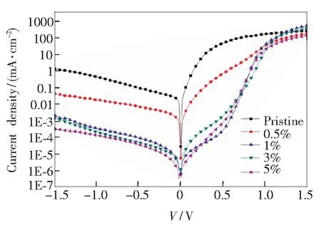
Fig.6 Current density-voltage characteristics of perovskite solar cells with different mass fraction of PNA additive in the dark
To obtain a deeply understanding of the perfect in device performance after dealing with different doping mass fractions of PNA additive, theJ-Vcharacteristics of the devices in dark conditions are measured and shown in Fig.6. The FF is an important parameter which perfected with the addition of PNA. The FF is controlled by both the parasitic series resistance (RS) and shunt resistance (RSH) of the solar cells[23-25]. TheRSandRSHof solar cells were calculated from the inverse of the slope of theJ-Vcurve at the open circuit voltage and short circuit conditionV=0, respectively. The dark condition current curve of the cell can mirror the changes of the cell’sRSandRSH. RepresentativeRSis controlled by the bulk conductivity of the electrodes, active and interfacial layers, and the contact resistance between them whileRSHis controlled by the quality of the films and their interfaces. During our research theRSandRSHwere leached by fitting theJ-Vcurves with Lambert W function to help to analyze the FF of different devices and the relevant data are summed up in Tab.1. When small quantity of PNA was added, a high FF over 69% was gained with both theRSandRSHincreased over the devices with original film. Taking the 1% PNA doped devices as an example, a lowRSof 5.77 Ω·cm2and a highRSHof 823.08 Ω·cm2were gained while the pristine film resulted a relatively highRSHof 12.02 Ω·cm2and a lowerRSHof 355.14 Ω·cm2. We advise that the rough edges of the abnormity perovskite crystal domains as surveyed by the SEM study may act as charge scattering centers which influence the charge transport property of the pristine film. While the well-defined crystal domains with smoother edges in the composite films could have better charge transport properties and therefore accounts for the decrease ofRS. However, at very high PNA doping concentration, theRSof the corresponding devices was increased again for the insulating property of the polymer additive. About theRSH, we define the PNA additive helps to form homogenous continuous films by fewer pinholes, which could avoid PEDOT∶PSS from directly contact with the PC61BM by the uncovered void area of the perovskite film. It refers that such a PEDOT∶PSS/PC61BM contact can develop shunting paths affects the diode characteristic and restricts theVocof the perovskite solar cells[26]. The great increase in theRSHimplied that the charge leaking at the anode interface was efficiently restrained. The perfected diode behavior of the PNA-doped devices can also be checked in the decreased dark current at the reversed bias region in theJ-Vplot as shown in Fig.6, resulting in devices with better rectification and FF.
4 Conclusion
To sum up, it is developed an innovative approach by utilizing the PNA additive to improve the performance of planar heterojuntion perovskite solar cells. The influence of PNA additives on perovskite film properties and photovoltaic performance were studied. The PNA additive can adjust the crystal-growth and coverage of perovskite thin-films, and accelerating the formation of continuous films with fewer pinholes and voids, which were back up by SEM measurement. In contrast with the corresponding normal device, an pronounced enhancement of PCE was achieved from 1.31% to 8.13% in the device utilizing an additive of 1%(mass fraction) of PNA. The good crystallization and higher surface coverage of perovskite film with PNA additive efficiently improve the charge transport and suppress charge recombination, therefore resulting in the obviously improvedVoc,Jscand FF for the solar cells.
[1] HEO J H, IM S H, NOH J H,etal.. Efficient inorganic-organic hybrid heterojunction solar cells containing perovskite compound and polymeric hole conductors [J].Nat.Photon., 2013, 7(6):486-491.
[2] BAO X C, ZHU Q Q, QIU M,etal.. High-performance inverted planar perovskite solar cells without a hole transport layerviaa solution process under ambient conditions [J].J.Mater.Chem. A, 2015, 3(38):19294-19298.
[3] ZHENG E Q, WANG X F, SONG J X,etal.. PbI2-based dipping-controlled material conversion for compact layer free perovskite solar cells [J].ACSAppl.Mater.Interf., 2015, 7(32):18156-18162.
[4] ZHANG F, YI C Y, WEI P,etal.. A novel dopant-free triphenylamine based molecular “butterfly” hole-transport material for highly efficient and stable perovskite solar cells [J].Adv.EnergyMater., 2016, 6(14):1600401-1-7.
[5] ZHAO Y C, WEI J, LI H,etal.. A polymer scaffold for self-healing perovskite solar cells [J].Nat.Commun., 2016, 7:10228-1-9.
[6] LI J F, ZHAO C, ZHANG H,etal.. Improving the performance of perovskite solar cells with glycerol-doped PEDOT∶PSS buffer layer [J].Chin.Phys. B, 2016, 25(2):028402-1-5.
[7] JEON S, THAKUR U K, LEE D,etal.. N-phenylindole-diketopyrrolopyrrole-containing narrow band-gap materials for dopant-free hole transporting layer of perovskite solar cell [J].Org.Electron., 2016, 37:134-140.
[8] JEON N J, NOH J H, KIM Y C,etal.. Solvent engineering for high-performance inorganic-organic hybrid perovskite solar cells [J].Nat.Mater., 2014, 13(9):897-903.
[9] LIU T F, LIU L F, HU M,etal.. Critical parameters in TiO2/ZrO2/carbon-based mesoscopic perovskite solar cell [J].J.PowerSources, 2015, 293:533-538.
[10] WU C G, CHIANG C H, HAN H C. Manipulating the horizontal morphology and vertical distribution of the active layer in BHJ-PSC with a multi-functional solid organic additive [J].J.Mater.Chem. A, 2014, 2(15):5295-5303.
[11] LI C, WANG F Z, XU J,etal.. Efficient perovskite/fullerene planar heterojunction solar cells with enhanced charge extraction and suppressed charge recombination [J].Nanoscale, 2015, 7(21):9771-9778.
[12] DONG Q Q, WANG Z W, ZHANG K C,etal.. Easily accessible polymer additives for tuning the crystal-growth of perovskite thin-films for highly efficient solar cells [J].Nanoscale, 2016, 8(10):5552-5558.
[13] WU Q L, ZHOU P C, ZHOU W R,etal.. Acetate salts as nonhalogen additives to improve perovskite film morphology for high-efficiency solar cells [J].ACSAppl.Mater.Interf., 2016, 8(24):15333-15340.
[14] HEO J H, SONG D H, IM S H. Planar CH3NH3PbBr3hybrid solar cells with 10.4% power conversion efficiency, fabricated by controlled crystallization in the spin-coating process [J].Adv.Mater., 2014, 26(48):8179-8183.
[15] EPERON G E, STRANKS S D, MENELAOU C,etal.. Formamidinium lead trihalide: a broadly tunable perovskite for efficient planar heterojunction solar cells [J].EnergyEnviron.Sci., 2014, 7(3):982-988.
[16] LIANG P W, LIAO C Y, CHUEH C C,etal.. Additive enhanced crystallization of solution-processed perovskite for highly efficient planar-heterojunction solar cells [J].Adv.Mater., 2014, 26(22):3748-3754.
[17] WEI Q B, YANG D, YANG Z,etal.. Effective solvent-additive enhanced crystallization and coverage of absorber layers for high efficiency formamidinium perovskite solar cells [J].RSCAdv., 2016, 6(62):56807-56811.
[18] KIM H S, LEE C R, IM J H,etal.. Lead iodide perovskite sensitized all-solid-state submicron thin film mesoscopic solar cell with efficiency exceeding 9% [J].Sci.Rep., 2012, 2:591-1-7.
[19] CONINGS B, BAETEN L, DE DOBBELAERE C,etal.. Perovskite-based hybrid solar cells exceeding 10% efficiency with high reproducibility using a thin film sandwich approach [J].Adv.Mater., 2014, 26(13):2041-2046.
[20] ZUO C T, DING L M. An 80.11% FF record achieved for perovskite solar cells by using the NH4Cl additive [J].Nanoscale, 2014, 6(17):9935-9938.
[21] CHANG C Y, CHU C Y, HUANG Y C,etal.. Tuning perovskite morphology by polymer additive for high efficiency solar cell [J].ACSAppl.Mater.Interf., 2015, 7(8):4955-4961.
[22] XUE Q F, HU Z C, SUN C,etal.. Metallohalide perovskite-polymer composite film for hybrid planar heterojunction solar cells [J].RSCAdv., 2015, 5(1):775-783.
[23] DING J L, RADHAKRISHNAN R. A new method to determine the optimum load of a real solar cell using the lambertW-function [J].SolarEnergyMater.SolarCells, 2008, 92(12):1566-1569.
[24] BLOM P W M, MIHAILETCHI V D, KOSTER L J A,etal.. Device physics of polymer: fullerene bulk heterojunction solar cells [J].Adv.Mater., 2007, 19(12):1551-1566.
[25] YIP H L, JEN A K Y. Recent advances in solution-processed interfacial materials for efficient and stable polymer solar cells [J].EnergyEnviron.Sci., 2012, 5(3):5994-6011.
[26] EPERON G E, BURLAKOV V M, DOCAMPO P,etal.. Morphological control for high performance, solution-processed planar heterojunction perovskite solar cells [J].Adv.Funct.Mater., 2014, 24(1):151-157.

李建丰(1976-),男,湖南湘潭人,教授,硕士生导师,2009年于兰州大学获得博士学位,主要从事有机光电功能材料与器件的研究。
E-mail: ljfpyc@163.com

夏养君(1973-),男,甘肃天水人,教授,博士生导师,2006年于华南理工大学获得博士学位,主要从事有机光电功能材料与器件的研究。
E-mail: xiayangjun2015@126.com
2016-12-05;
2017-01-24
国家自然科学基金(51602139,61404067,51463011); 甘肃省自然科学基金(1310RJZA076)资助项目 Supported by National Natural Science Foundation of China(51602139,61404067,51463011); Natural Science Foundation of Gansu Province(1310RJZA076)
利用PNA添加剂来调控钙钛矿薄膜结晶和覆盖率实现高效太阳能电池
李建丰1, 吕 杰1, 赵 创1, 彭一春2, 李彩娟3, 夏养君1*
(1. 兰州交通大学 光电技术与智能控制教育部重点实验室, 甘肃 兰州 730070;2. 兰州工业学院 土木工程学院, 甘肃 兰州 730050; 3. 兰州工业学院 电气工程学院, 甘肃 兰州 730050)
钙钛矿薄膜形貌的控制是一个提高太阳能电池能量转换效率的关键问题,而引入添加剂是解决这一问题的一种有效而简便的方法。利用聚丙烯腈(PNA)作为CH3NH3PbI3前驱体溶液溶剂添加剂,通过其浓度可以调控钙钛矿薄膜结晶和表面的覆盖率。本文通过SEM、XRD以及UV-Vis研究了PNA掺杂CH3NH3PbI3钙钛矿薄膜后的表面形貌、结晶度和光学性能的变化。结果表明,通过添加少量的PNA可以优化钙钛矿薄膜的性能,其强烈影响薄膜的结晶过程,有助于形成均匀连续的薄膜,减少针孔,从而增强了钙钛矿层的覆盖率和光吸收。当PNA 的含量为1%(质量分数)时,钙钛矿太阳能电池的各项性能最佳,能量转换效率达到了8.38%。与未加PNA 的电池效率(1.31%) 相比,提高了540%。这些结果表明,PNA可以有效调控钙钛矿薄膜的晶体生长和薄膜形貌,在钙钛矿太阳能电池的大规模生产过程中是一种可以改善钙钛矿薄膜质量的有效添加剂。
聚丙烯腈; 添加剂; 晶体生长; 钙钛矿太阳能电池
1000-7032(2017)07-0897-08
O649.4 Document code: A
10.3788/fgxb20173807.0897
*Corresponding Author, E-mail: xiayangjun2015@126.com
猜你喜欢
黄河之声(2021年8期)2021-07-23
中国石油石化(2021年10期)2021-07-16
学生天地(2020年29期)2020-06-09
学生天地(2020年31期)2020-06-01
学生天地(2020年19期)2020-06-01
学生天地(2020年19期)2020-06-01
学生天地(2019年30期)2019-08-25
物理学进展(2017年1期)2017-02-23
云南师范大学学报(自然科学版)(2015年5期)2015-12-26
太阳能(2015年4期)2015-02-28