
Modulation depth of series SQUIDs modified by Josephson junction area∗
2017-08-30 08:26JieLiu刘杰HeGao高鹤GangLi李刚ZhengWeiLi李正伟KamalAhmadaZhangYingShan张颖珊JianSheLiu刘建设andWeiChen陈炜
Chinese Physics B 2017年9期
Jie Liu(刘杰),He Gao(高鹤),Gang Li(李刚),Zheng Wei Li(李正伟), Kamal Ahmada,Zhang Ying Shan(张颖珊),Jian She Liu(刘建设),and Wei Chen(陈炜),†
1 Tsinghua National Laboratory for Information Science and Technology,Department of Microelectronics and Nanoelectronics, Institute of Microelectronics,Tsinghua University,Beijing 100084,China
2 Key Laboratory of Particle Astrophysics,Institute of High Energy Physics,Chinese Academy of Sciences,Beijing 100049,China
3 University of Chinese Academy of Sciences,Beijing 100049,China
Modulation depth of series SQUIDs modified by Josephson junction area∗
Jie Liu(刘杰)1,He Gao(高鹤)2,3,Gang Li(李刚)1,Zheng Wei Li(李正伟)2, Kamal Ahmada1,Zhang Ying Shan(张颖珊)1,Jian She Liu(刘建设)1,and Wei Chen(陈炜)1,†
1 Tsinghua National Laboratory for Information Science and Technology,Department of Microelectronics and Nanoelectronics, Institute of Microelectronics,Tsinghua University,Beijing 100084,China
2 Key Laboratory of Particle Astrophysics,Institute of High Energy Physics,Chinese Academy of Sciences,Beijing 100049,China
3 University of Chinese Academy of Sciences,Beijing 100049,China
The superconducting quantum interference device(SQUID)amplifier is widely used in the field of weak signal detection for its low input impedance,low noise,and low power consumption.In this paper,the SQUIDs with identical junctions and the series SQUIDs with different junctions were successfully fabricated.The Nb/Al-AlOx/Nb trilayer and input Nb coils were prepared by asputtering equipment.The SQUID devices were prepared by a sputtering and the lift-off method. Investigations by AFM,OM and SEM revealed the morphology and roughness of the Nb films and Nb/Al-AlOx/Nb trilayer. In addition,the current–voltage characteristics of the SQUID devices with identical junction and different junction areas were measured at 2.5 K in the He3refrigerator.The results show that the SQUID modulation depth is obviously affected by the junction area.The modulation depth obviously increases with the increase of the junction area in a certain range.It is found that the series SQUID with identical junction area has a transimpedance gain of 58 Ω approximately.
superconducting quantum interference device(SQUID),Josephson junction,transition edge sensor
1.Introduction
Superconducting transition edge(TES)detectors have been adopted as bolometric detectors for millimeter[1,2]and submillimeter wavelength detection owing to their good performance on noise,response speed,linearity,and the fact that they can be fabricated into large arrays and read out by multiplexing techniques.[2–7]Moreover,the years since 2005 have also witnessed the emergence and applications of complete x-ray and γ-ray spectrometers based on arrays of superconducting transition-edge sensors(TESs).[8]A superconducting quantum interference device(SQUID)can be used to read out a transition edge sensor(TES)because of its low noise,low input impedance,and high resolution.[6,9–14]The reason why the gain of a single SQUID amplifier is too small to read out the transition edge sensor is that the voltage noise of a typical DC SQUID is about two orders of magnitude lower than the input noise of the best room temperature amplifier.[15–18]There are mainly two solutions to the problem.One is to use a series SQUID amplifier.[13]The other is a two-stage series array of SQUID amplifiers which is made of a single SQUID and an array of SQUID amplifiers.[13,15]In addition,the modulation depth has a pronounced effect on the performance of series SQUID.[16,19,20]The modulation depth can be affected by the screening parameter(βL),junction area,and shunt resistor.Therefore,it is very important to investigate the performance of the series SQUID.However,there is little detailed comparison analysis of the series SQUID electrical properties, particularly in the aspect of modulation depth,for different McCumber–Stewart parameter(βc)modified by the Josephson junction area.
In this report,we present the influence of the McCumber–Stewart parameter βcmodified by the Josephson junction area on the modulation depth.Through the series SQUID amplification,it can accomplish a higher transimpedance gain.The critical current,modulation curve,and amplification gain of SQUID corresponding to different junction areas have been investigated.The relationship among modulation depth,junction area,and critical current is studied experimentally.The electrical characteristics of four series SQUID devices are also tested.
2.Fabrication and testing
2.1.Device design and fabrication
We successfully fabricated a 2-inch device wafer,as shown in Fig.1(a),which consists of the typical series SQUIDs cell,as shown in Fig.1(b).Figure 2(a)is the optical micrograph of a typical series SQUID device.Figure 2(b) shows the typical electric circuit of the series SQUID ampli-fi er corresponding to Fig.2(a).During the fabrication of the SQUID amplifier,the Josephson junction as the basic component has a crucial effect on the device.We choose the Josephson junction of Nb/Al-AlOx/Nb trilayer structure as the basic element of SQUID.Because this sandwich structure can be achieved via ultra-high vacuum sputtering,avoiding air pollution,thus ensuring the formation of a high-quality barrier structure.At the same time,Al can be used as a natural blocked layer for reactive ion etching during junction definition and the preparation of through-holes,which is helpful to precisely control the etching depth during the fabrication process.The five steps of the photolithography process to fabricate the Josephson junction and SQUID process are as follows.
(i)A 400 nm thick SiO2film is grown by thermal oxidation on the surface of a 2-inch〈100〉crystalline N-type singlesided polished Si wafer.Considering that the SiO2layers are very thin,prior to the lithography,they are cleaned by an ultrasonic cleaning method with acetone and alcohol to ensure that there are no residual organics and air pollutants which may cause device failure.
(ii)Trilayer deposition A Nb/Al-AlOx/Nb trilayer is deposited over an entire oxidized-Si wafer and patterned to defi ne the SQUID washer,capacitors,and bonding pads.This layer can be easily and quickly patterned using a lift-off method.
(iii)Junction definition This step is used to pattern the shape of the Josephson junction.The second lithography is carried out through the negative photoresist NR9-3000PY, which aims to define the junction area on the three-layer film surface.Then,the top Nb films are etched by ICP5100 with SF6.Afterwards,the deposited SiO2film can be used as the dielectric insulator,which could isolate the Josephson junction bottom electrode and the Nb wiring layer.It should be noted that the NR9-3000PY employed during the lithography process may cause the exposure area to exhibit an inverted trapezoid,which in turn results in that the obtained Josephson junction area is smaller than the design value.This can be manifested in Subsection 3.2.
(iv)Depositing resistor layer Pt resistor is mainly used to eliminate the hysteresis of the Josephson junction,thus achieving a single value of over-damping Josephson junction. The Pt shunt resistors are deposited by a sputtering equipment and patterned using a lift-off stencil.The Pt layer is deposited by Lab18 sputtering equipment.The typical sheet resistance is 0.6–0.9 Ω/square.Before sputtering Pt,we need to sputter a layer of Ti with a thickness of 8 nm in order to increase the surface adhesion.
(v)Depositing Nb wiring layer A Nb wiring layer is deposited and patterned to define the modulation coil (10µm linewidth),interconnects,and feedback coil(10µm linewidth).The Nb wiring layer is patterned using a lift-off stencil.A de-oxidation process is performed prior to sputtering the upper electrode with a thickness of 260 nm.

Fig.1.(color online)(a)Fabricated SQUID device wafer.(b)A typical series SQUID cell.
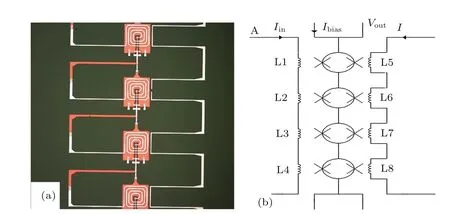
Fig.2.(color online)(a)The typical optical micrograph of series SQUID device.(b)The typical electric circuit of series SQUID amplifier.
2.2.Device testing
The Josephson junction and SQUID performance tests are carried out in a Janis He3refrigerator,mainly consisting of four temperature zones,namely,296 K,40 K,3 K,and 0.3 K.The SQUID test is mainly carried out at 3 K.The detailed device testing system has been described in our previous report.[19]
3.Results and discussion
3.1.Morphology and topography of Nb and trilayer films
The Nb,Nb/AlOx,and Nb/AlOx/Nb films fabricated under the conditions described above have been characterized by AFM.Figure 3 shows the morphology of Nb,Nb/AlOx, and Nb/AlOx/Nb trilayer deposited on silicon oxide substrates. The trilayer film is very smooth,though the roughness is increased with the increase of the layers,as can be seen from Fig.3.The detailed deposition parameters are listed in Table 1. The surface roughness is 0.698 nm,1.04 nm,and 1.29 nm for the layers of Nb,Nb/AlOx,and Nb/AlOx/Al/Nb,respectively, based on the AFM.
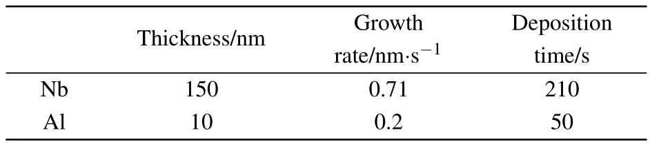
Table 1.Deposition parameters of films.

Fig.3.(color online)AFM photographs of(a)Nb film,(b)Nb/AlO x,(c)Nb/AlO x/Nb layer.(d)Morphology of Nb/AlO x with the area of 5µm×5µm.
3.2.Series SQUID characteristics with different junction areas
Figure 4 shows the SEM photographs of the fabricated series SQUID amplifiers with different junction areas.As can be seen from Fig.4,there is a deviation between the design value and the actual size.This phenomenon is due to the exposure area as discussed in Subsection 2.2.The size of the fabricated devices is not the same as the designed layout exactly.Detailed actual dimensional values of the SQUIDs are listed in Table 2.

Table 2.Parameters of fabricated series SQUID amplifiers.The 1st SQUID,2nd SQUID,3rd SQUID,and 4th SQUID are corresponding to the red circles from left to right shown in Fig.4(a).
Figure 5 shows the I–V characteristics of series SQUIDs with different junction areas.It can be seen that the critical current is increased with the junction area increasing from 5.3µm2to 22.5µm2.The critical current density is 270–300 A/cm2.
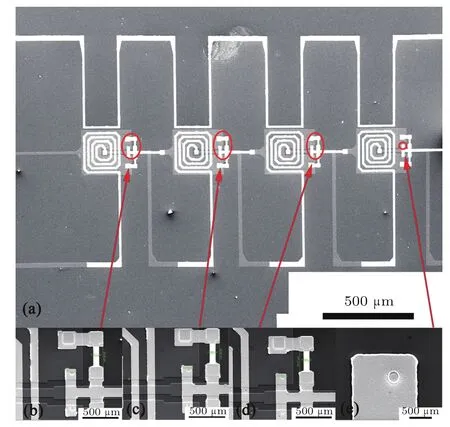
Fig.4.(color online)(a)SEM photographs of fabricated series SQUID amplifiers with different junction areas.The detailed structure and practical junction area corresponding to the red circle in each SQUID:(b) 22.5µm2,(c)15.9µm2,(d)8.2µm2,(e)5.3µm2.
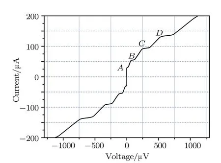
Fig.5.(color online)The critical current of series SQUIDs with different junction areas.A:5.3µm2,B:8.2µm2,C:15.9µm2,D:22.5µm2 (the critical currents are 30µA,50µA,84µA,and 124µA,respectively).
Figure 6 shows the modulation curve of SQUIDs with different junction areas under varying bias currents.The bias currents chosen are 31.28µA,51.01µA,88.59µA,and 130.51µA for junction areas of 5.3µm2,8.2µm2,15.9µm2, and 22.5µm2,respectively,according to the I–V characteristics shown in Fig.5.It can be seen that the modulation period of the SQUID with different Josephson junction area is about 8.3µA,which is because the same mutual inductance due to the same washer structure and the turns of input coils. But it should be noted that the modulation depth,as shown in Fig.6,is increased as the junction area increases,which is 13µV,32µV,66µV,and 106µV.For simplicity,the modulation depth can also be estimated as follows:


where ΔV is the modulation depth,Ic0is the critical current, and Φ0is the magnetic flux quantum.According to Eqs.(1) and(2),the detailed calculation results are listed in Table 3.It can be observed that the experimental results are in agreement with our theoretical calculation as shown in Fig.7.Figure 8 shows the amplification curves of SQUIDs with junction areas of(a)3.46µm2,(b)5.72µm2,(c)15.9µm2,(d)22.8µm2.As can be seen in Fig.8,the input current(peak-to-peak)value is 2µA,the output voltage(peak-to-peak)is 7.6µV,13.5µV, 31µV,and 61µV,which means that the derived SQUID amplifier gain could be 3.8 Ω,6.45 Ω,15.5 Ω,and 31.5 Ω,respectively.
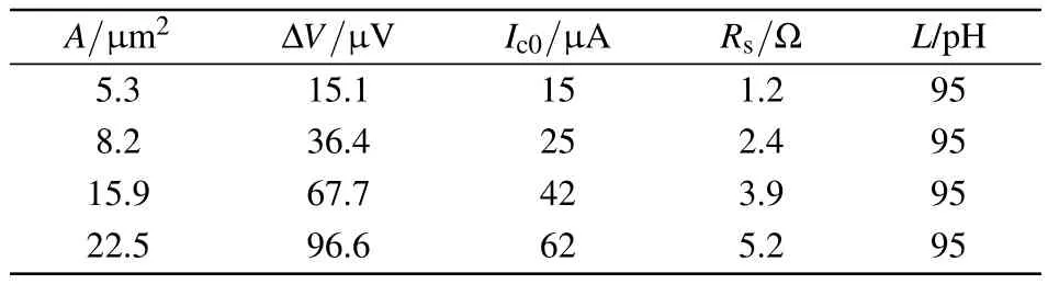
Table 3.The calculated modulation depth ΔV of SQUIDs with different Josephson junction areas A.

Fig.6.(color online)Modulated curve of series SQUIDs with different junction areas under different bias currents.The bias current based on the different junction area is 31.28µA(5.3µm2),51.01µA(8.2µm2), 88.59µA(15.9µm2),130.51µA(22.5µm2)for different junction area.The corresponding modulation depth is 13µV,32µV,66µV, and 105µV,respectively.
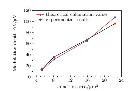
Fig.7.(color online)Comparison of experimental results and theoretical calculation values of modulation depth of SQUIDs with different Josephson junction areas.

Fig.8.(color online)Amplification curves of SQUIDs with different junction areas of(a)5.3µm2,(b)8.2µm2,(c)15.9µm2,(d) 22.5µm2.
3.3.Series SQUID characteristics with identical junction area
As shown in Subsection 3.2,there exists a highest modulation depth when the Josephson junction of SQUID has an area of 22.5µm2.However,it should be pointed out that the McCumber–Stewart parameter(βc=1)lies in a critical state. As reported by Clarke et al.,[16,17]for the under damped junctions with βc>1,the relationship between current and voltage in the hysteresis region is not a single valued function. To avoid this under damped situation and to obtain a relatively high amplification gain,it would be better to fabricate series SQUIDs with identical junction area of 15.9µm2in our study.

Fig.9.(color online)Photographs of fabricated series of SQUID amplifier with identical junction area of 15.9µm2 wire bonding onto a PCB circuit board.

Fig.10.(color online)(a)Critical current of four series SQUIDs with the same junction area.(b)Amplification curve of four series SQUIDs with identical junction area.
Figure 9 displays a series SQUID consisting of four identical SQUIDs with the junction area of 15.9µm2bonding onto a PCB circuit board.As can be seen from Fig.10(a),the critical current is about 90µA under these circumstances.As shown in Fig.10(b),the input current peak-to-peak value is 1µA,the output voltage peak-to-peak value is 58µV,indicating that the SQUID amplifier gain is derived as 58 Ω,which is in accordance with the results above,four times of amplification gain of single SQUID with an area of 15.9µm2,as shown in Fig.8(c).
4.Conclusion
The series SQUIDs have been designed and fabricated successfully.The trilayer Nb/Al-AlOx/Nb fabricated by sputtering in Ar atmosphere is quite smooth.It is found that the high quality Josephson junction with stable critical current density can be produced via this fabrication process.By variation of the junction area,the amplification gain is increased from 3.8 Ω to 31.5 Ω for each single SQUID.As for the four series SQUIDs with the identical Josephson junction area,the amplification gain can be up to 58 Ω.
[1]Lee A T,Richards P L,Nam S W,Cabrera B and Irwin K 1996 Appl. Phys.Lett.69 1801
[2]Zhang Q Y,Wang T S,Liu J S,Dong W H,He G F,Li T F,Zhou X X and Chen W 2014 Chin.Phys.B.23 118502
[3]Li H,Zhang S L,Qiu Y,Zhang Y S,Zhang C X,Kong X Y and Xie X M 2015 Chin.Phys.B.24 028501
[4]Qiu Y,Liu C,Zhang S L,Zhang G F,Wang Y L,Li H,Zeng J,Kong X Y and Xie X M 2014 Chin.Phys.B 23 088503
[5]Schwan D,Bertoldi F,Cho S,Dobbs M,Guesten R,Halverson N, Holzapfel W,Kreysa E,Lanting T and Lee A 2003 New Astron.Rev. 47 933
[6]Irwin K D and Hilton G C 2005 Cryogenic Particle Detection(New York:Springer)p.63
[7]Irwin K 1995 Appl.Phys.Lett.66 1998
[8]Ullom J N and Bennett D A 2015 Supercond.Sci.Technol.28 084003
[9]de Korte P A,Beyer J,Deiker S,Hilton G C,Irwin K D,MacIntosh M,Nam S W,Reintsema C D,Vale L R and Huber M E 2003 Rev.Sci. Instrum.74 3807
[10]Irwin K,Niemack M,Beyer J,Cho H,Doriese W,Hilton G,Reintsema C,Schmidt D,Ullom J and Vale L 2010 Supercond.Sci.Technol.23 034004
[11]Mates J,Hilton G,Irwin K,Vale L and Lehnert K 2008 Appl.Phys. Lett.92 023514
[12]Chervenak J,Irwin K D,Grossman E N,Martinis J M,Reintsema C D and Huber M 1999 Appl.Phys.Lett.74 4043
[13]Huber M E,Neil P A,Benson R G,Burns D A,Corey A M,Flynn C S, Kitaygorodskaya Y,Massihzadeh O,Martinis J M and Hilton G 2001 IEEE T.Aaapl.Supercon.11 1251
[14]Prˆele D,Voisin F,Piat M,Decourcelle T,Perbost C,Chapron C,Rambaud D,Maestre S,Marty W and Montier L 2016 J.Low Temp.Phys. 184 363
[15]Tuttle J,DiPirro M,Shirron P,Welty R and Radparvar M 1996 Cryogenics 36 879
[16]Clarke J and Braginski A I 2004 The SQUID Handbook Vol.1 p.34
[17]Clarke J,Goubau W M and Ketchen M B 1976 J.Low Temp.Phys.25 99
[18]Tesche C D and Clarke J 1977 J.Low Temp.Phys.29 301
[19]Chen Z,He G F,Zhang Q Y,Liu J S,Li T F and Chen W 2015 Acta Phys.Sin.64 128501(in Chinese)
[20]Weinstock H 2012 SQUID Sensors:Fundamentals,Fabrication and Applications.(Berlin:Springer Scienceamp;Business Media)
29 March 2017;revised manuscript
24 May 2017;published online 18 July 2017)
10.1088/1674-1056/26/9/098501
∗Project supported by the National Natural Science Foundation of China(Grant No.11653001),the National Basic Research Program of China(Grant No.2011CBA00304),and Tsinghua University Initiative Scientific Research Program,China(Grant No.20131089314).
†Corresponding author.E-mail:weichen@tsinghua.edu.cn
©2017 Chinese Physical Society and IOP Publishing Ltd http://iopscience.iop.org/cpb http://cpb.iphy.ac.cn
猜你喜欢
Chinese Physics B(2022年11期)2022-11-21
大江南北(2022年11期)2022-11-08
大江南北(2022年3期)2022-03-12
辽河(2022年2期)2022-03-03
书香两岸(2020年3期)2020-06-29
北方音乐(2019年13期)2019-08-21
Chinese Physics B(2019年6期)2019-06-18
美与时代·美术学刊(2018年10期)2018-01-25
汉语世界(2017年5期)2017-09-21
中国学术期刊文摘(2016年3期)2016-02-14

- Chinese Physics B的其它文章
- Improved control for distributed parameter systems with time-dependent spatial domains utilizing mobile sensor actuator networks∗
- Geometry and thermodynamics of smeared Reissner–Nordström black holes in d-dimensional AdS spacetime
- Stochastic responses of tumor immune system with periodic treatment∗
- Invariants-based shortcuts for fast generating Greenberger-Horne-Zeilinger state among three superconducting qubits∗
- Cancelable remote quantum fingerprint templates protection scheme∗
- A high-fidelity memory scheme for quantum data buses∗