Synthesis of Nb Doped Few-layered MoS2 by Ambient Pressure CVD
2018-12-13 12:51SHENHeWANGYanyan
发光学报 2018年12期
SHEN He, WANG Yan-yan
(1. Key Laboratory of Functional Materials Physics and Chemistry, Ministry of Education, Jilin Normal University, Changchun 130103, China; 2. College of Physics, Jilin Normal University, Siping 136000, China; 3. Key Laboratory of Preparation and Application of Environmental Friendly Materials, Ministry of Education, Jilin Normal University, Changchun 130103, China; 4. College of Chemistry, Jilin Normal University, Siping 136000, China) *Corresponding Author, E-mail: shenhe861206@163.com
Abstract: Base on the ambient pressure CVD method, the large-scale Nb doped few-layered MoS2 films were synthesized by using NbCl5 powders as the Nb dopant source. The morphology and the thickness of these films were confirmed by scanning electron microscope and atomic force microscope. Raman spectroscopy and X-ray photoelectron spectrometer measurements confirm that Nb has been doped into the MoS2 film and the Nb doped MoS2 alloy has been formed. The conductivity of the Nb doped few-layered MoS2 has also been collected.
Key words: ambient pressure CVD; MoS2 film; Nb doped
1 Introduction
Layered transition metal dichalcogenides(TMDCs) such as MoS2, MoSe2, WS2and WSe2have recently emerged as promising materials for low cost, flexible and transparent electronics and optoelectronics applications, owing to their unusual physical, optical, and electrical properties arising from the quantum confinement associated to their ultrathin structure[1-4]. For example, MoS2demonstrates many “graphene-like” properties including a relatively high carrier mobility(a field effect mobility of ~200 cm2·V-1· s-1for the monolayer), mechanical flexibility(up to 11% strain), chemical and thermal stability, and moreover when the dimension of MoS2is reduced from a three-dimensional bulk form into a two-dimensional(2D) sheet, the band gap transforms from an indirect to a direct one (Egof ~1.8 eV for the monolayer), which makes them a semiconducting alternative to gapless graphene[5-6].
Doping is widely used to adjust carrier densities and tailor the electronic characteristics of semiconductors, which is more significant in case of 2D materials. The electrical property of monolayer TMDCs materials can be modified by electrostatic doping and adsorption of dopants[3-4,7]. However, the implementation of these methods cannot enable the permanent or stable doping effects in doped layers and is not convenient for practical device applications. Among TMDCs, the doping of MoS2has been studied earlier and has more basis in the experiments and theoretical descriptions[8-11].Niobium(Nb) has been considered as most promising p-type dopant of MoS2by calculating the formation energies and the electronic properties of many possible doping element[12]. And the inclusion of Nb into MoS2occupies part positions of Mo changes little the bond lengths and also the main density of state. Moreover, Nb doping of MoS2occurs through a substitutional mechanism has also been speculated by using density-functional theory[13]. Note that experimental studies show that Nb-substituted MoS2nanoparticles and Nb doped MoS2thin film can be synthesized, and that they also exhibit p-type character[14]. Reference to these results, p-type few-layered MoS2may be doped by using Nb related chemicals as dopants.
An ambient pressure chemical vapor deposition (CVD) growth method for the synthesis of niobium disulfide(NbS2) nanosheets by reacting Niobium chloride(NbCl5) with sulfur(S) vapor has been reported[15]. Coincidentally, CVD method and S vapor are commonly used in the growth of monolayer MoS2with molybdenum oxide(MoO3). So Nb doped monolayer MoS2is very hopeful to be obtained in CVD technique by employing MoO3powder and S powder as Mo and S sources, NbCl5precursors as Nb dopant sources. However, no experimental report exists for this speculation, which is necessary for demonstration of substitutional doping in few-layered MoS2.
In this letter, the Nb doped few-layered MoS2has been prepared by using an ambient pressure CVD method. Raman spectroscopy, X-ray photoelectron spectrometer(XPS), scanning electronmicroscope(SEM) and atomic force microscope(AFM) imaging indicated that Nb has been doped into MoS2, the size of the doped MoS2film is up to several millimeters and the thickness of it is only about 1 nm. The conductivity of the Nb doped few-layered MoS2is p type.
2 Experiments
The samples investigated in this letter were all grown inside a quartz-tube in an ambient pressure CVD technique employing Si/SiO2(285 nm SiO2) as the substrates, the growth schematic is shown in Fig.1. The MoO3powders were dispersed into ethanol, and then dropped onto the surface of a quartz plate. S and NbCl5powders in different quartz plates were used as S source and Nb dopant. The substrate was pre-cleaned and placed in the downstream region inside the quartz tube. The quartz tube were mounted on a furnace. The number of red solid circulars indicates different heating temperature. The quartz tube was first evacuated to a base pressure of 100 Pa(1 mbar), followed by a 20 mL/min flow of Ar argon gas(with H25%) as carrier gas. The MoO3heating zone was ramped to 550 ℃ in 20 min, then to 850 ℃ in 40 min, and the S heating zone was ramped to 210 ℃ in 40 min. The temperature of MoO3and S heating zones maintained at 850 ℃ and 210 ℃ for 40 min and 60 min, respectively. NbCl5powder was put at the edge of S heating zone far away from the substrates. The furnace was cooled to room temperature naturally after the growth. The morphology and the thickness of the Nb doped MoS2films were measured in a JEOL JSM-6700F field emission scanning electron microscope(SEM) and a Neaspec Atomic force microscopy(AFM). Raman spectrum at excitation wavelength of 532 nm was analyzed in a Renishaw Invia Raman microscope. An AXIS Ultra ‘DLD’ X-ray photoelectron spectrometer(XPS) was used to collected chemical bonding state in the films.

Fig.1 CVD setup for the growth of the Nb doped few-layered MoS2 alloy
3 Results and Discussion
Fig.2 shows the SEM photograph of the Nb doped MoS2film. The large-scale film has been obtained and the size of it is up to several millimeters. One can see that there are numerous triangle-shaped crystals at the edge of the film, which are the Nb doped MoS2crystals have not linked up into a film. The height of this film is determined to be only about 1 nm from AFM measurement as shown in the inset.

Fig.2 SEM image of the Nb doped few-layered MoS2 alloy, and the inset shows the AFM height signal of the alloy film.

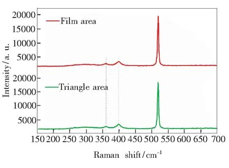
Fig.3 Raman spectra collected from the Nb doped MoS2 film and triangle-shaped crystal areas
To further prove the above speculation, the XPS measurement was carried out to different areas of the Nb doped MoS2film, as shown in Fig.4. We can see from the figure that the Nb 3d spectra change little in different areas, which are all close to the spectra of NbxMo1-xS2nanoparticles(x=0.25)[14]. One can deduce from the above data that Nb has been doped into the MoS2film, the Nb doped MoS2alloy has been formed. The electrical properties of the film areas were also measured, the Nb doped
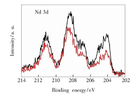
Fig.4 XPS spectra of Nb 3d in different areas of the Nb doped MoS2 film
MoS2film shows p-type conductivity, but the mobility of this film is only about 2.5 cm2·V-1·s-1, which is much lower than the expected value for the MoS2monolayer. The low mobility may be influenced by too much Nb doped and also the crystallization quality, that must be improved in the following work.
4 Conclusion
In summary, large-scale few-layered Nb doped MoS2films have been fabricated in an ambient pressure CVD technique by employing NbCl5as doping precursor. The form of the Nb doped MoS2alloy films has been confirmed, the conductivity of the obtained films is p-type. We note that although the mobility of these films is still lower than the expected value, this doping method may provide a way to go for efficient p-type MoS2doping.