Active Current Sharing of LCLC Resonant Converter with Switch-Controlled-Capacitor Technology
2020-04-27 14:20LIUYanfei,HEXiaobin
上海航天 2020年2期
Abstract:In this paper,an interleaved LCLC converter with enhancement-mode(E-mode)GaN devices is introduced to achieve the accurate current sharing performance for data center applications.Any tolerance in the resonant tank elements can lead to large load imbalance between any two different phases.Due to the steep gain curves of LCLC converters,conventional current sharing methods are not effective.In the proposed converter,the impedances of the resonant networks are matched by switching a capacitor,i.e.,switch controlled capacitor(SCC),in series with the resonant capacitor in one or some of the phases,which results in accurate load current sharing among the phases with an accuracy around 0.025%.The load share of a phase is sensed through the resonant current on it,and the control logic applied to such current sharing can be achieved.By this method,accurate current sharing is achieved for a wide input voltage range required for the hold-up time in data center applications.Interleaving is applied in the proposed multiphase LCLC converter,resulting in low current stress on the output capacitor and allowing ceramic capacitor implementation.Moreover,phase shedding accomplishes high light load efficiency.The performance of the proposed interleaved LCLC converter is verified by a two-phase 1 kW prototype with an input voltage ranging from 250 V to 400 V and a fixed 12 V output voltage.
Key words:interleaved multiphase resonant converter;current sharing;switch controlled capacitor(SCC);TO-220 enhancement-mode(E-mode)GaN;high electron mobility transistor(HEMT);data center
0 Introduction
In recent years,the electrical demands of data centers have massively increased due to the fast development of information technology and cloud computing.Considering that data center services are still in a nascent stage,the power conversion capability should keep up with the growing electric demands.With the advancements in power electronics technology,more electric energy can be transferred to consumer loads in data centers.Soft switching technology has good power characteristics,e.g.,zero voltage switching(ZVS)and zero current switching(ZCS).Due to the low voltage requirements of the server motherboard bus,LLC resonant converters have been widely used as front-end converters for data centers,which can convert 400 V direct current(DC)buses to 12 V ones.The obtained 12 V DC buses are then connected to load converters to supply CPU,memory and so on[1-3].
In data center applications,it is required for the DC-DC converters to be able to operate in a wide input voltage range to provide power during the hold-up time in case of AC line failures.It has been reported that an LCLC resonant converter demonstrates an improved hold-up performance compared with an equivalent LLC resonant converter[3].Another issue in data center applications is the high current level(such as 80 A)on the low-side bus,the voltage of which is 12 V,limiting the power level of resonant converters used in data centers to 1 kW and below 12 V output.
Hence,it is required to parallel several resonant converters to distribute their power stress and increase their current capability.By implementing phase interleaving,the input and output filters of the resonant converter can be designed with a small capacitance.To ensure the good effect of phase interleaving,the current sharing performance should be studied precisely because the capacitors and inductors used in the resonant tanks have tolerances and the voltage gain of the resonant converters varies with the impedance of the resonant network.Thus,any small imbalance in the voltage gain of one phase can cause significant current imbalance among the individual phases.Unequal loading of phases is a critical problem in interleaved resonant converters because it reduces the converter efficiency,causes thermal imbalance,and can lead to converter failures under severe load conditions.
Various passive and active current sharing methods have been proposed for multiphase LLC converters.In[4-7],different passive and automatic impedance matching(PIM)methods including common-inductor and common-capacitor approaches were studied thoroughly for different resonant tanks.The PIM method is quite effective in current sharing as it does not require additional components and control schemes.However,the current sharing performance will be compromised when there are random positive and negative tolerances in all the resonant components.Moreover,in most of passive current sharing methods,phase shedding cannot be implemented to increase the light load efficiency.
In[8],a single integrated magnetic was used in a three-phase LLC converter to balance the current sharing.Like other integrated magnetic based methods,this method is not effective in current balancing when the converter is operating in a wide input voltage.In[9],a current sharing approach was performed for an interleaved LLC converter by adjusting the duty cycle of the phase carrying higher load share.Although,in this method,only a new control method is needed,the duty cycle cannot be reduced too much to compensate for large tolerances and converters with a wide operating range.In[10-11],current sharing was done by adding one or two power switches in each phase to switch in and out a capacitance or inductance in the resonant tank to compensate the gain difference between phases.This method provides a precise way of adjusting the current between phases at the expense of additional components.However,the additional power devices do not have any switching losses and there are only switch conduction losses.Therefore,it does not compromise the efficiency noticeably.
In this paper,the switch controlled capacitor(SCC)method is implemented in a wide input voltage resonant converter.,the SCC method is flexible to interleave any number of phases and implement phase shedding to improve efficiency profiles,it and efficient to do PCB windings for magnetics to achieve fixed inductances for wide input range resonant converters.It approach is a better solution than any conventional method which can handle large tolerances for interleaved LCLC converters.The SCC method has never been studied for any resonant converter with a steep voltage gain to investigate the accuracy of current sharing.In this paper,the half-wave SCC is implemented on the phases of a wide operating range two-phase LCLC converter.
The rest of this paper is organized as follows.In the next section,the characteristics of different parts of the proposed SCC-LCLC resonant converter are analyzed.In Section 2,the control method and current sharing performance are discussed.In Section 3,practical considerations using GaN high electron mobility transistors(HEMTs)are provided.The experimental results of a laboratory prototype are provided in Section 4.Finally,the main conclusions are summarized in Section 5.
1 SCC-LCLC resonant converter
1.1 LCLC resonant converter
As mentioned before,a wide input voltage range is a desired feature for front-end DC-DC converters to satisfy the required hold-up time,especially in data center applications.If the variation of the input voltage range is too great,the LLC converter performance can be deteriorated.With LLC network,a small magnetizing inductor is needed to meet the voltage gain requirement when the input voltage is low,which will increase the circulating current and the root-mean-square(RMS)current at the primary side through magnetics and switches leading to the increase in the conduction power loss.To find a suitable solution for the wide input voltage range,a modified LLC resonant converter called LCLC resonant converter is proposed in[3].The LCLC resonant converter is consisted of two resonant inductors(LrandLp)and two resonant capacitors(CrandCp),and is theoretically equivalent to an LLC resonant converter with variable magnetizing inductance.The topology of a half-bridge LCLC resonant converter with full-wave rectifier is shown in Fig.1,whereCinis the input filter capacitor,Cois the input filter capacitor,andRLis load.
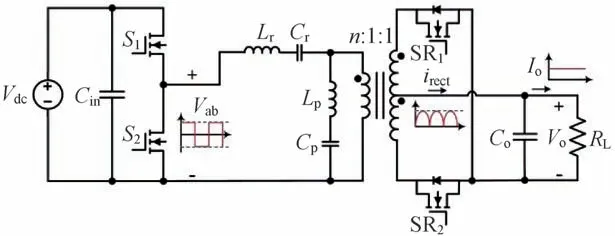
Fig.1 Schematic diagram of the half-bridge LCLC resonant converter
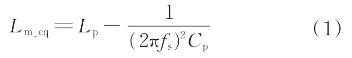
The equivalent magnetizing inductor of the LCLC resonant converter can be changed by changing the switching frequency.The desired magnetizing inductor is implemented by a series connected parallel inductor(Lp)and capacitor(Cp).The resonant components can be selected through the design procedure of the LCLC converter based on the input voltage range,where the output voltage and current are the same as those described in[3].After the design procedure,the equivalent magnetizing inductor(Lm_eq)at different switching frequencies can be calculated as follows:
The voltage gain of the LCLC resonant tank can be calculated by substituting(1)in the voltage gain expression of the LLC resonant tank as follows:
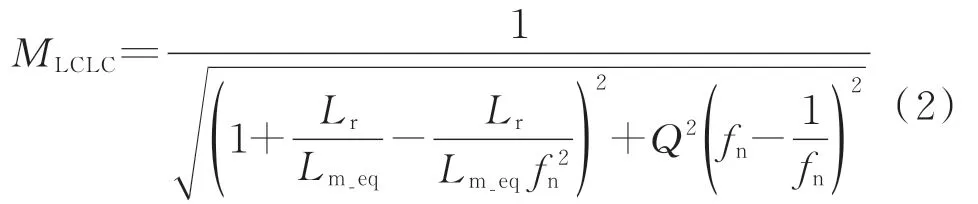
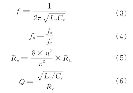
where the series resonant frequency(fr),the normalized frequency(fn),the equivalent output resistance of the LCLC converter transferred to the primary of the transformer(Re),and the quality factor(Q)are as follows:
The voltage gain characteristics of LCLC and LLC resonant tanks are demonstrated in Fig.2.In order to get the same switching frequency variation for a specific required voltage gain in both resonant tanks,a 70 μH magnetizing inductance is needed for the LLC resonant tank.However,the magnetizing inductance in the LCLC resonant tank may be higher than that of the LLC tank,and the equivalent magnetizing inductance is variable.When the input voltage is high,the required voltage gain is low.Therefore,the switching frequency can be designed to be around the resonant frequency,in which the magnetizing inductance is large.Hence,the RMS current at the primary side can be reduced compared with an equivalent LLC converter.Moreover,when the input voltage is low,the required voltage gain is high,and thus the switching frequency becomes lower and is close to the parallel resonant frequency.In this case,the magnetizing inductance is small enough to allow high voltage gain.
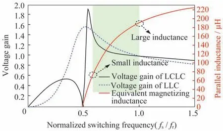
Fig.2 Voltage gain characteristics of LCLC and LLC resonant tanks along with changeable equivalent magnetizing inductance
Figure 2 shows that the voltage gain curve of the LCLC resonant tank is much steeper than the voltage gain curve of the LLC resonant tank.Therefore,the value of the voltage gain is more sensitive to the variation of the switching frequency in the LCLC converter,which makes the current imbalance problem due to the resonant tank element tolerances of an LCLC resonant converter much worse than that of an LLC resonant converter.Hence,in order to actively and accurately tune the voltage gain,a switch controlled capacitor should be implemented to solve the current sharing problem.
1.2 Half-wave SCC
The half-wave SCC circuit consists of a capacitorCain parallel with a metal-oxide-semiconductor fieldeffect transistor(MOSFET)Sa(see Fig.3).The switchSais connected to a low side driver as it shares a common source with the main bridge switches.
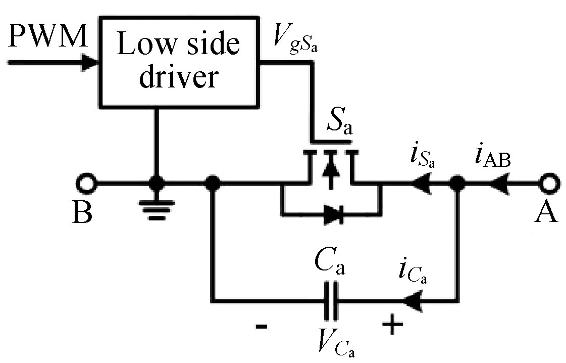
Fig.3 Schematic diagram of the half-wave SCC circuit
Figure 4 shows the half-wave SCC operation waveform.The operation principle of the SCC circuit is described as follows.Assume that a sinusoidal currentIABis flowing through the SCC and the current zero-crossing points are at angles 0,π,2π,… SwitchSais turned off at the angle 2nπ+α.AfterSais turned off,the current flows from A to B viaCaand charges the capacitor until it reaches the next current zerocrossing point at(2n+1)π.Then,the current reverses its direction,and begins to dischargeCa.AfterCais fully discharged,the negative current is about to flow from B to A via the body diode ofSa.To prevent its body diode from conducting,Sais turned on.It remains on for the rest of cycle and is turned off again at the angle(2n+2)π+α.Figure 5 shows the relationship between the series resonance capacitance(Cs)and the angleαunder different conditions ofCa.
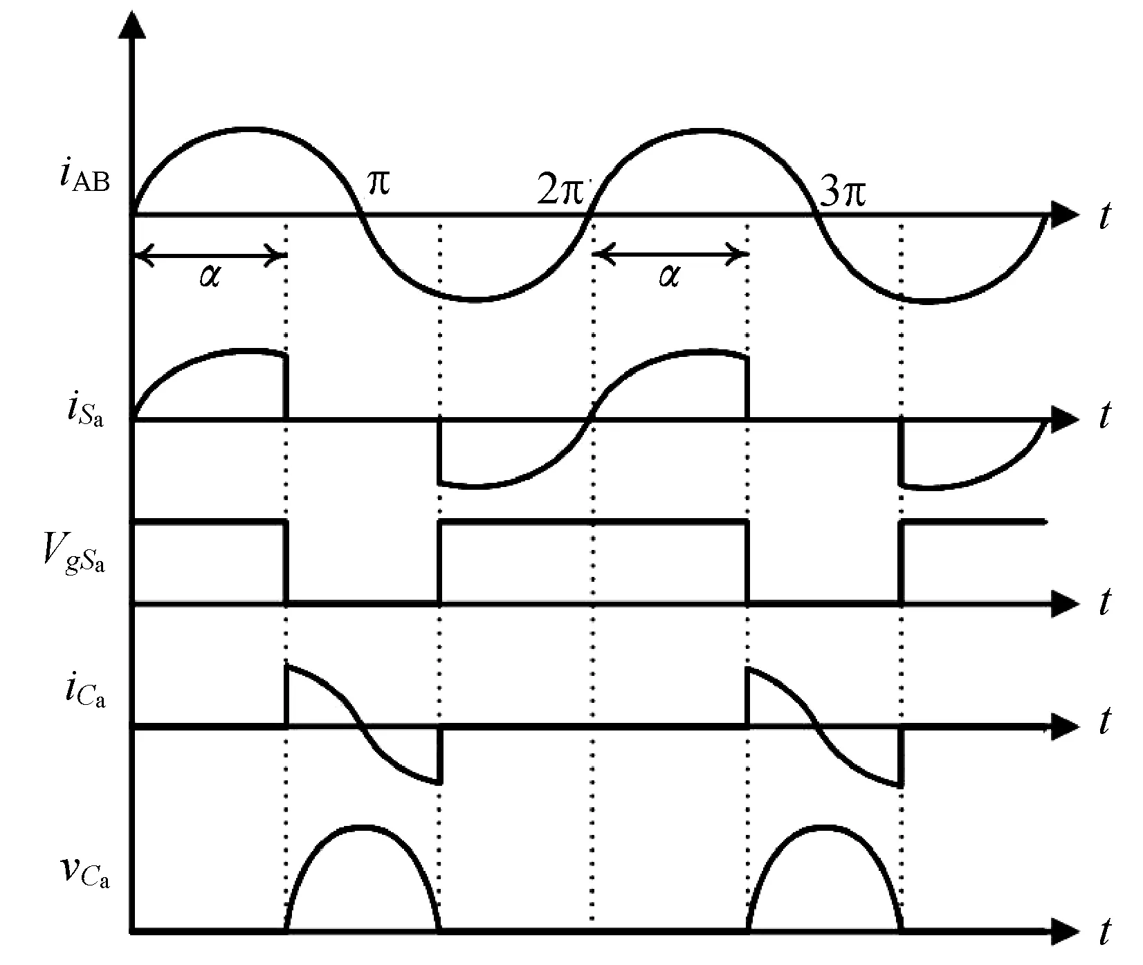
Fig.4 General waveforms of the half-wave SCC with sinusoidal current

Fig.5 Variations of the series resonant capacitance(Cs)via the angle α(Cr=20 nF)
The equivalent SCC capacitanceCSCCis modulated by the delay angleα,and can be expressed as follows:
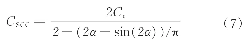
whereCais the SCC parallel capacitor.The equivalent series resonant capacitanceCs(CSCC in series withCr)can then be derived as follows:

whereCris the resonant capacitor of the original tank.
The angleαvaries from 0 to π,which correspond to the minimum and maximum values of the resonant capacitance.Whenα=0,the currentIABwill flow throughCaand bypass the SCC MOSFET.Thus,the equivalent resonant capacitance is at its minimum value,which is equal to the value ofCrandCaconnected in series.Whenα=π,currentIABwill flow through the SCC MOSFET and bypass the capacitorCa,which makes the equivalent resonant capacitance toward its maximum valueCr.In other word,SCC can change the equivalent resonant capacitor by varying the delay angleαso as to compensate the tolerance through reducing the equivalent series resonant capacitanceCs.
1.3 Interleaved SCC-LCLC resonant converter
Figure 6 shows the schematic diagram of the two-phase LCLC converter with SCC circuit implemented on both phases.By employing SCC on both phases,any random imbalance can be compensated by both SCC circuits,and a reliable performance can be achieved.SwitchesSa1andSa2are half-wave SCC MOSFETs switching in and out the SCC capacitors,i.e.,Ca1andCa2,to compensate the resonant current by achieving an equal voltage gain with the same switching frequency for both phases.Two current transformers,i.e.,CT1andCT2,are used for the current zero crossing detection required for the synchronization of the SCC gate pulse for each phase as well as the resonant current measurement required for the current sharing performance and SCC gate pulse generation(α1andα2).All these data will go into an MCU,and correct gate pulses will be generated for the SCC MOSFETs.More details of the control strategy and SCC operation will be provided in the next section.

Fig.6 Schematic diagram of the proposed interleaved SCC-LCLC resonant converter
2 Control and current sharing performance of the proposed SCC-LCLC converter
In the SCC-LCLC converter,the resonant current of each phase is sensed by a current transformer to find out the level of load shared among different phases.Then,based on the control algorithm shown in Fig.7(bottom,left part),the proper command to increase or decrease the angleαof each phase is generated in the MCU.In order to reduce the impact of the SCC operation on the original LCLC converter,it is desired to increase the angleαof the higher current phase first and then decrease the angleαof the other phase.In order to turn on the SCC MOSFET at the right time,it is necessary to find out the zero-current crossing(ZCC)point of the resonant current,which can be implemented by the same current transformer used for the current level measurement.The output voltage of the SCCLCLC converter is regulated by a frequency-controlled passive impedance(PI)loop.The basic waveforms of the SCC-LCLC converter including the SCC operation are shown in Fig.8.In these waveforms,it is assumed that the load current in Phase 2 is lower than that in Phase 1,and more SCC compensation is required for Phase 2.

Fig.7 Control scheme of the proposed SCC-LCLC converter
In resonant converters,when the load is changed,the voltage gain characteristic curve changes,and hence the RMS current of the resonant current changes.Thus,in order to see the effect of theangleαon the current sharing performance,the RMS value of the resonant current of all phases should be investigated.For simplicity,it is considered that the operating point is at resonance(fs=fr)and the resonant inductor current is pure sinusoidal.The resonant current can be written as follows:

whereILr_RMSis the resonant RMS current.
The magnetizing current can be written as follows:
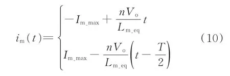
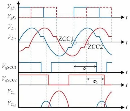
Fig.8 Key operational waveforms with the proposed SCCconverter
The peak value of the magnetizing current can be calculated as follows:

To comply with the assumption made at the beginning of the analysis,the equivalent magnetizing(Lm_eq)inductance should be calculated at the resonant frequency according to the above equations.The RMS resonant current can be calculated from the energy transferred to the load as follows:

By changing the angleαon a phase,the equivalent resonant capacitor in that phase changes,the voltage gain and the output voltage change,and so does the resonant RMS current.Thus,using(2),the relationship between the resonant current and the resonant components can be expressed as follows:

As shown in Fig.2,small values of the SCC capacitor and small delay angles ofαcan change the series resonant capacitance a lot,leading to a significant change in the half-cycle resonant frequency,which can adversely affect the performance of the resonant converter by making it asymmetrical.Asymmetrical operation is not desirable in resonant converters as it can reduce the turn-on time of only one leg of input switches and SRs and hence increase the power loss and decrease the conversion efficiency.Therefore,small values ofαshould be avoided.In practice,a moderate value ofαbetween 100° and 170° is desirable.In Fig.9,the effects of the switching frequency and the delay angleαon the resonant current are plotted.As can be observed,the variation of the resonant current is the largest when the SCC compensation is relatively large(e.g.,α=100°)and the switching frequency is low(e.g.,near peak gain).
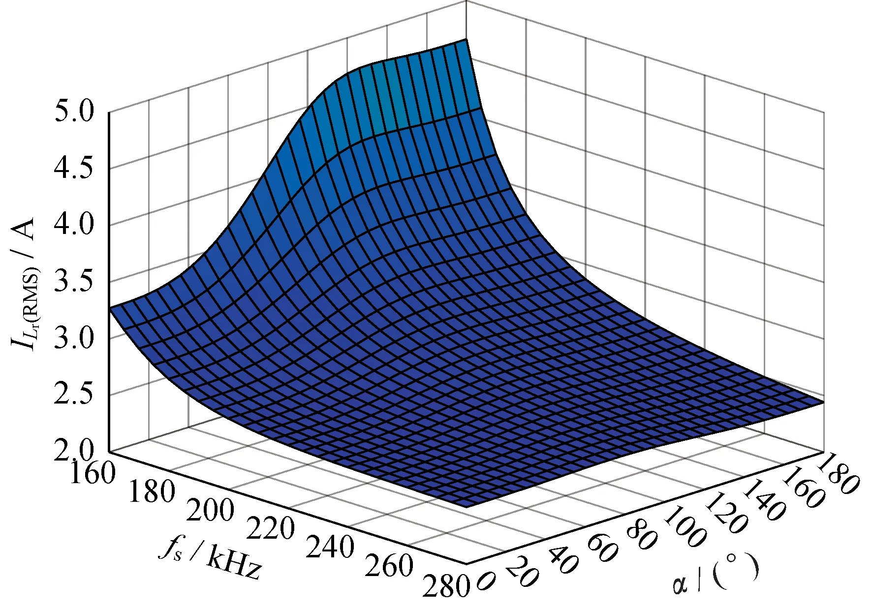
Fig.9 A 3D plot of the resonant RMS current variation due to the changes in the switching frequency(fs)and the angle α(with Ca=20 nF)
In order to see the accuracy of the current sharing,the effect of the smallest change inαcan be observed on the resonant RMS current change.Using the design method proposed in[3]for the following input parameters:Vin_min=250 V,Vo=12 V,Po=500 W,andfs_min=175 kHz,in order to have a large enough compensation range,we selectLr=12 μH,Cr=20 nF,Lp=230 μH,Cp=5 nF,andn=18 for the power circuit of the LCLC converter andCa=20 nF andα1=α2=100° for the SCC circuit.With 1 ns change in the duty cycle,the delay angleαvaries by 0.066°.Therefore,the smallest change inαonly for Phase 2 leads toα2=100.066°.Then,the RMS current difference(ΔILr)can be calculated using(13)as follows:

The maximum accuracy in the current sharing by this method using a 16 bits MCU is around 0.028%.A simulation setup is built in the PSIM software.The same parameters are used for calculations,and the calculation accuracies are compared.The resonant current waveforms and the RMS values are shown in Fig.10.From Fig.10,we can see that the simulation results are consistent with the theoretical analysis.The difference in the resonant RMS current from the simulation is ΔILr=0.001 13 A,and the current sharing accuracy can reach 0.023%.The difference between the RMS values taken from the calculation and simulation is because of the first harmonic approximation in the analytical calculations leading to inaccuracy at frequencies below the resonant frequency.

Fig.10 Simulated results for the resonant RMS currents of the inductors Lr1 and Lr2
3 Practical implementation consideration using GaN HEMT devices
Switching devices play a key role in designing new high efficiency converters for data center applications.GaN HEMTs have small gate charges(Gg)and output capacitances(Coss)compared with typical Si devices.GaN devices demonstrate various benefits in high frequency soft-switching resonant converters from several aspects.In general,a large enough dead time is required for switches to achieve ZVS in resonant converters.The longer dead time reduces the effective turn-on time of the switch in a cycle,and hence increase the RMS current through the switch and magnetic windings,which will increase the power loss.Moreover,by increasing the switching frequency,the deadtime needs to be reduced,and hence a higher magnetizing current is required to achieve ZVS,which requires for a smaller magnetizing inductance.This will increase the circulating current and power loss.By using GaN HEMTs,shorter dead time of switching can be used with larger magnetizing inductance,smaller air gap,and less fringing loss in the windings,because the switching speed of GaN switch is much faster than that of Si switch.Moreover,compared with Si switch,CaN switch has no body diode,so it is a perfect choice for resonant converters under light load conditions,of which the reverse recovery loss is almost zero and there is no need to extend the dead time of switching under light load to maintain ZVS operation[12-13].
In earlier generation of GaN devices,many manufactures used depletion-mode(D-mode)GaNs in cascode structure to make a normally off device by a series connection of a low voltage Si field-effect transistor(FET)and a high voltage D-mode GaN HEMT.This configuration is motivated by a reasonably high threshold gate voltage,a small output capacitance,a low reverse recovery charge,and a conventional TO package with good thermal performance and ease of use.However,the cascode configuration compromises the superior performance of single device GaNs.Recently,enhancement-mode(Emode)GaN devices have been widely used by manufacturers and researchers all over the world due to their superior performance such as high transition speed,low drain source turn-on resistance,and reverse conduction with no reverse recovery.Most of E-mode GaN HEMTs come in small surface mount packages from different manufacturers.Although the small packaging can bring low parasitic inductance,the thermal performance is a critical issue,especially for high power applications[12-14].Recently,E-mode GaN devices with the TO package are manufactured to take the advantages of all benefits of surface mount GaNs as well as good thermal management due to the metal tab available for heat sinking.Because of the addition of Si FETs in cascode GaNs,the parasitic package inductances of both surface mount and through-hole packages are higher than those of Emode GaNs.Nowadays,E-mode GaNs are the mainstream wide band gap(WBG)switching devices in the industry due to their superior performance over other WBG devices.
Among all parasitic components,the common source inductance(CSI)shared by both driving and power loops is the most significant one because of its direct effects on the gate driving performance and consequent power loss or gate breakdown[14].During the presence of high di/dt,a voltage will be created on the CSI which can reduce the gate-to-source voltage and hence prevent the optimal use of the fast switching capability by slowing down the switching time.This is very important in hard-switching converters as the switching loss is directly affected by the switching speed.In resonant converters,ZVS operation is always sought at the turn-on moment.During the dead time,when GaN is in the reverse conduction state,the negative current level will be very low,so it is usually considered to adopt a marginal ZVS operation design to reduce the circulating RMS current through the circuit.Hence,there is no high di/dtduring the actual turn-on transition and the voltage drop on the gate is not noticeable.However,during the turn-on interval,an LCR resonant tank is formed among the CSI,the gate capacitance,and the gate resistance which should be damped in order to avoid positive voltage ringing across the gate(see Fig.11).The voltage ringing could exceed the threshold voltage and cause shoot-through by unwanted turn-on of the GaN.This can be alleviated by increasing the damping effect either by increasing the gate resistance or adding a small ferrite bead to the gate.
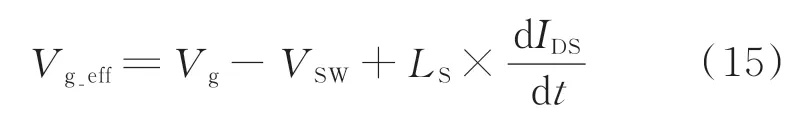
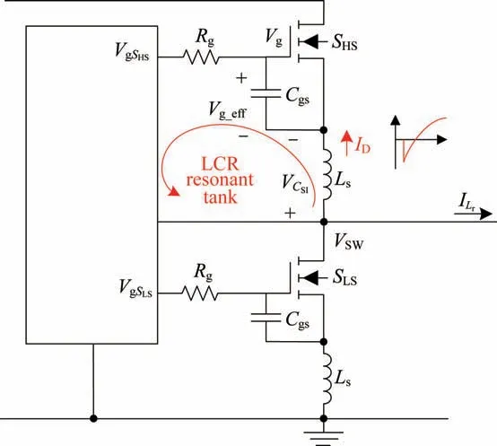
Fig.11 CSI effect on the gate drive performance
In this study,650 V E-mode GaN HEMTs in the TO-220 package from GaN power international Inc.[15]are used in a 500 W LCLC resonant converter and compared with a GaNpxTMpackage from the GaN systems in the same design[16].In the test setup,only air cooling is used for thermal dissipation,and no heat sink is used for the GaN devices.The current rating of the implemented GaNs with the TO-220 package is 15 A and the current rating of the GaNpxTMpackage is 60 A.The thermal images of both GaN devices are shown in Fig.12 with 400 V and 12 V output voltages at 40 A.As can be seen in Fig.12,the temperatures of both GaNs are around 40°with fan cooling.It is deemed that using surface mount GaNs may lead to over design and thus reduce the condition loss and meet the same heat dissipation requirement as in an otherwise-identical design with through-hole GaNs.Hence,if the resonance on the gate voltage is properly alleviated,the TO-220 GaN package will be a good candidate for high power applications since the high parasitic inductance of a TO package is not a big concern forresonant converters because of the ZVS switching and small di/dtat the turn-on moment.
4 Experimental results
A 1 kW experimental prototype is built in the laboratory with the design parameters listed in Tab.1.Figure 13 shows the experimental setup using the“device under test”(DUT)under full-load conditions.When E-mode GaN HEMTs with the TO-220 package are used in the proposed converter,the SCC MOSFET and synchronous rectifiers(SRs)are also used with the TO-220 package in this prototype for consistency.It has been observed that the performance of through-hole SRs with the TO-220 package is relatively similar to surface mount counterparts and the negative effects due to the higher output capacitance can be curbed by using a small RCD noise filter[17].Moreover,the magnetics are intentionally made with different values for both phases to count for severe imbalance conditions.Figure 14 shows the steady-state resonant current waveforms with an input voltage of 400 V at half load and full-load conditions.As can be seen from Fig.14,after applying the SCC circuit,the resonant current is actively balanced among both phases under different load conditions.Because the layout of the secondary side circuit does not allow a direct current measurement of the output current of each phase,the current sharing performance between these two phases are compared through the resonant current.The voltages of the SCC capacitor for both phases are below 20 V,and the voltage is larger in Phase 2 to compensate the current imbalance.

Tab.1 Parameters used in the prototype

Fig.13 Photo of the laboratory prototype under test
Figure 15 shows the steady state resonant current of both phases with the 250 V input voltage under half-load and full-load conditions.It can be seen that the SCC capacitor voltage in Phase 1 is larger in this case to compensate for the gain difference.The maximum SCC capacitor voltage is around 70 V in this case with the 250 V input voltage and under the full load condition.The difference of the SCC capacitor at 400 V and 250 V input voltages is due to that Fig.15 the higher gain curves and lower switching frequencies require higher gain compensation when the input voltage is 250 V.
Furthermore,the output capacitor voltage ripple and the temperature are compared for interleaved and non-interleaved modes in Fig.16.By applying 90°C phase interleaving,the output capacitor voltage ripple and the current ripple are reduced significantly.It can be seen that the output voltage ripple is reduced to less than a half and the output capacitor temperature(TCo)is reduced from 61°C to 46°C under the 400 V input voltage condition.The reduction in the output capacitor current ripple leads to the reduction in the power loss occurred in the output capacitor,resulting in the increase in the efficiency.Figure 17 shows the efficiency curve for the 400 V input voltage with and without phase shedding.It is clear that the proposed converter can achieve a flat efficiency curve over a wide input voltage and load range with an efficiency over 96%,a load range from 15 A to 80 A,and the peak efficiency of 96.7%.

Fig.15 Steady state waveforms with the 250 V input voltage under half-load and full-load conditions
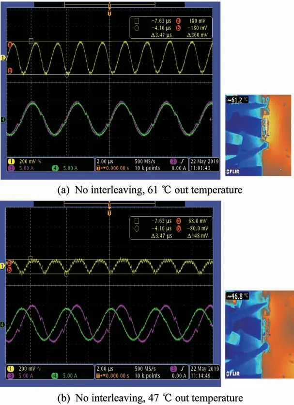
Fig.16 Experimental results for the resonant current waveforms,theoutput capacitor voltage ripple,and the temperature of the output capacitor(TCo)

Fig.17 Efficiency curves for the 400 V input voltage with(green)and without(dark blue)phase shedding over a wide load range
5 Conclusions
In this paper,an interleaved LCLC resonant converter with current sharing for a wide operating range is proposed.With the converter,accurate current sharing is achieved by implementing an SCC technology,and the accuracy of current sharing can be as high as 0.025% in theory.The current sharing performance is verified through experimental results for half-load and full-load conditions for both 250 V and 400 V input voltages.The non-interleaved and interleaved operations of the proposed converter are compared.The results show that the output capacitor temperature is reduced by 15 °C by interleaving,and the proposed converter can achieve a flat efficiency curve over a wide load range with a peak efficiency of 96.7%.