
Super-resolution imaging of low-contrast periodic nanoparticle arrays by microsphere-assisted microscopy∗
2021-05-06 08:54QinFangShi石勤芳SongLinYang杨松林YuRongCao曹玉蓉XiaoQingWang王晓晴TaoChen陈涛andYongHongYe叶永红
Chinese Physics B 2021年4期
Qin-Fang Shi(石勤芳), Song-Lin Yang(杨松林), Yu-Rong Cao(曹玉蓉),Xiao-Qing Wang(王晓晴), Tao Chen(陈涛), and Yong-Hong Ye(叶永红),‡
1Department of Physics,Nanjing Normal University,Nanjing 210023,China
2Advanced Photonics Center,Southeast University,Nanjing 210096,China
3Jiangsu Provincial Key Laboratory of Advanced Robotics,Soochow University,Suzhou 215123,China
Keywords: super-resolution,microsphere,optical microscopy,surface plasmon polariton
1. Introduction
Overcoming the Abbe diffraction limit has been a strong driving force of biomedical researches in the past two decades. Researches on super-resolution microscopy have been developed rapidly,emerging various technologies such as stimulated emission depletion microscopy,[1]photo-activated localization microscopy,[2]stochastic optical reconstruction microscopy,[3]structured illumination microscopy,[4]scattering lens microscopy,[5]far-field superlens,[6]the hyperlens,[7]and microsphere-assisted microscopy.[8]Many techniques rely upon the contrast by fluorescent stains attached to the object of interest. This causes limitations due to the impact of the label on the object and its environment, as well as its applicability in vivo.
The microsphere-assisted microscopy is an emerging label-free technique for achieving super-resolution at very low intensities,which is useful for bio-imaging. In this technique,a microsphere is placed on an object in front of the objective. A magnified virtual image with the participation of the object’s optical near-fields is formed by the microsphere,and the microscope is used to observe the virtual image through the microsphere.[9]Super-resolution imaging has been experimentally realized in high-contrast samples,[9–19]and a resolution ∼λ/6–λ/7 has been demonstrated for label-free imaging nanoplasmonic structures.[14]Label-free super-resolution imaging of low-contrast objects remains difficult.[20]Biological tissues are low-contrast objects.[21]On the other hand,Wang et al. found that the magnification was ∼2× while imaging blu-ray disks, and the magnification was ∼8×(with a resolution around 50 nm) while imaging Au coated porous alumina structures.[9]Li et al. successfully imaged unlabeled 75-nm virus placed on a glass slide coated with a 5-nmthick gold film.[22]Recently,our group reported the label-free super-resolution imaging of dielectric nanoparticle arrays by assembling the arrays on a glass slide deposited with a 50-nm-thick Ag film.[23]It is proposed that the excitation of surface plasmon polaritons (SPPs) on the sample surface or at the substrate/sample interface plays an important role in the enhanced resolution.[24,25]These studies demonstrated that by depositing a metallic layer on the surface of a low-contrast sample[22]or placing the sample on a plasmonic or a metallic layer coated substrate,[26,27]the resolution and contrast in microsphere-assisted microscopy imaging of low-contrast objects can be improved.However,the differences in imaging by depositing a metallic on the sample surface or using a metallic layer coated substrate to hold the sample have not been studied. In this paper,we use hexagonally close-packed(hcp)unlabeled polystyrene(PS)nanoparticle arrays with nanoparticle diameters of 300 and 250 nm as low-contrast samples,and study the differences in imaging the sample prepared by the above methods. We find that when we deposit a 30-nmthick Ag film on the surface of a PS nanoparticle sample,and an array of PS nanoparticles with a diameter of 250 nm can be resolved. If we assemble a PS nanoparticle sample on a glass slide deposited with a 30-nm-thick Ag film,and only an array of 300-nm-diameter PS nanoparticles can be discerned.The 300-nm-diameter or 250-nm-diameter nanoparticle sample placed directly on a glass slide cannot be resolved.
2. Experimental methods
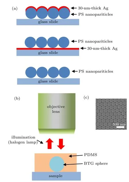
Fig.1. (a) Schematic of methods M1–M3. (b) Schematic of the experimental setup. (c) SEM image of an array of 250-nm-diameter PS nanoparticles.
Unlabeled hcp PS nanoparticle (n = 1.6) arrays with diameters of 300 and 250 nm are used in the experiments.Figure 1(a) is the schematic of the methods used to prepare samples. Method M1 is to place a sample on a glass slide and then deposit a 30-nm-thick Ag film on the surface of the sample. Method M2 is to place a sample on a glass slide coated with a 30-nm-thick Ag film. Method M3 is to place a sample directly on a glass slide. The thickness of the deposited Ag film is 30 nm because the reflectance of a 30-nm-thick Ag film is already ∼90% in the visible wavelength region.After the sample was prepared, we dropped BaTiO3glass(BTG)microspheres(Cospheric,n=1.95)with a diameter of about 30µm on the surface of the sample,and fully immersed the BTG microspheres in polydimethylsiloxane (PDMS), a method first proposed by Darafsheh et al.[12,28]The size of the BTG microspheres will affect the imaging properties,[29]such as the imaging contrast, magnification, and field of view. By balancing the above factors,we usually use BTG microspheres with a diameter around 15–30 µm in our experiments.[16]Finally, the sample was placed under a microscope (Leica DM2500M) in the reflection mode, and the virtual image of the sample magnified by the BTG microsphere was observed by an objective lens(100×,NA=0.9). Figure 1(b)illustrates the schematic of the experimental setup. Figure 1(c) is the Scanning Electron Microscope (SEM, JEOL JSM-5610LV)image of an array of PS nanoparticles. It shows that the PS nanoparticles are hcp. An Oceanoptics-USB4000 spectrometer was used to measure the reflectance spectra of the samples.
3. Results and discussion
We first use the microsphere-assisted microscopy to image periodic PS nanoparticle arrays with a nanoparticle diameter of 300 nm. While observing an object, the image of the object can be observed over a range of focused image plane. Figures 2(a1)–2(a4) are images of a PS nanoparticle array treated by method M1 at different focus image planes.The z value in the lower left corner indicates the distance from the image plane to the initial image plane(the imaging depth).Figure 2(a) shows that the PS nanoparticle array can be resolved. The imaging depth is about 8µm,and the magnification of the image in the entire imaging depth is around 2.73–2.93×. In addition, we also observe the Talbot effect of the periodic PS nanoparticle array. The nanoparticles are bright in Fig.2(a2),they are dark in Fig.2(a3),and they are bright again in Fig.2(a4). The images of an array of 300-nm-diameter PS nanoparticles prepared by method M2 at different focus image planes are shown in Figs.2(b1)–2(b3).Figure 2(b)reveals that the PS microsphere array can also be discerned. The image magnification in the entire imaging depth is 2.57–2.78×, and the imaging depth is around 5µm. Figure 2(c)plots the light intensity profile along straight lines drawn through the centers of two adjacent PS nanoparticles in Figs.2(a)and 2(b),and the measured full width at half maximum(FWHM)of an imaged PS nanoparticle is about 128 and 148 nm,respectively.
We also use PS nanoparticle arrays with a nanoparticle diameter of 250 nm as samples.Figures 3(a)and 3(b)are images of an array of 250-nm-diameter PS nanoparticles prepared by methods M1 and M2, respectively, at different focus image planes.The PS nanoparticle array prepared by method M1 can be observed(Fig.3(a)). The magnification in the entire imaging depth is 2.9–3.2×, and the imaging depth is about 9 µm.The PS nanoparticle arrays in Fig.3(b) can barely be seen.Figure 3(c) is the light intensity profiles along straight lines drawn through the centers of two adjacent PS nanoparticles in Figs. 3(a) and 3(b). The FWHM of an imaged PS nanoparticle in a nanoparticle array prepared by method M1 is about 117 nm. As the PS nanoparticle array prepared by method M2 cannot be resolved,the FWHM of the PS nanoparticle cannot be obtained.
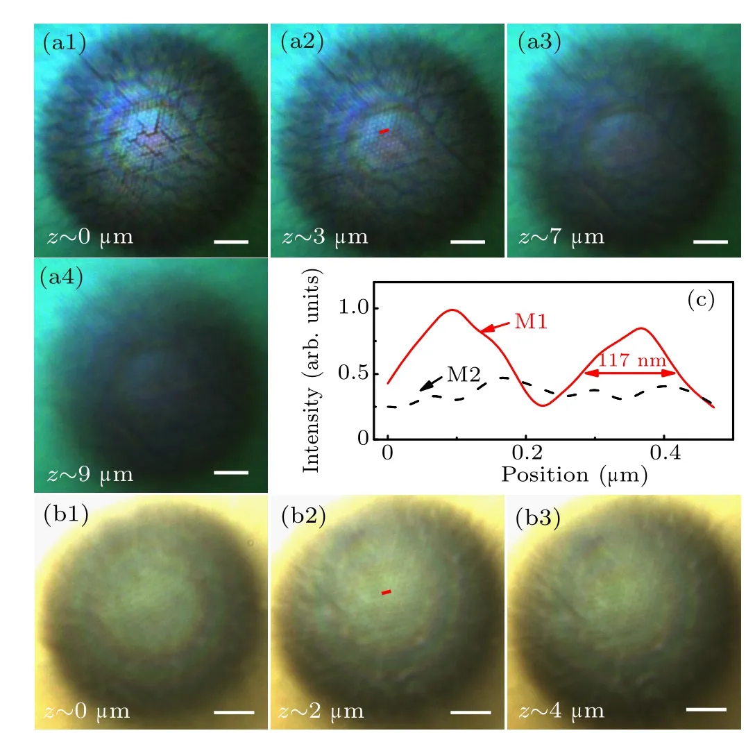
Fig.3.Images of an array of 250-nm-diameter PS nanoparticles prepared by different methods at different image positions. (a)Method M1. (b)Method M2. (c)Intensity profiles along straight lines drawn through the centers of two adjacent PS nanoparticles in the center of (a) (red solid line) and (b)(black dashed line). The scale bars are all 5µm.
We also use the label-free microsphere-assisted microscopy technique to image arrays of PS nanoparticles with a diameter of 300 nm directly placed on a glass slide(method M3),and find that these samples cannot be distinguished. For comparison, we also use a classical microscope without the aid of BTG microspheres to observed PS nanoparticle arrays with a diameter of 300 nm prepared by methods M1–M3,and find that the arrays cannot be resolved.
The experimental results of Figs.2 and 3 show that compared with standard microscopy,imaging low-contrast objects with label-free microsphere-assisted microscopy can enhance the resolution. In microsphere-assisted microscopy imaging,if an hcp PS nanoparticle array is prepared by methods M1 and M2,the resolution in imaging the array can be enhanced.Moreover, imaging a nanoparticle array prepared by method M1 has a higher resolution and a longer imaging depth than imaging a nanoparticle array prepared by method M2.
To understand the differences in imaging nanoparticle arrays prepared by different methods, we measured reflectance spectra of PS nanoparticle arrays by a spectrometer (Ocean Optics,USB4000)in the 380–700 nm wavelength range at an incident angle of 7◦. Figures 4(a)and 4(b)are the reflectance spectra of a PS nanoparticle array with a nanoparticle diameter of 300 and 250 nm, respectively, prepared by methods M1 (solid lines) and M2 (dashed lines). Figure 4(a) shows that for the 300-nm-diameter sample prepared by method M1,two dips λb= 401 nm and λc= 505 nm appear in the reflectance curve. Using method M2, there is only one dip(λa=424 nm) in the reflectance curve. The position of the dips of the 250 nm sample appears with a blue shift compared to the 300 nm sample. The two dips in the reflectance curve of the sample prepared by method M1 appear at λe=405 nm and λf=467 nm, respectively. In method M2, there is only one dip(λd=399 nm)in the reflectance spectrum.
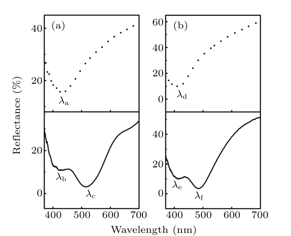
Fig.4.Reflectance spectra of an array of PS nanoparticles with different nanoparticle diameters prepared by methods M1 and M2: (a) 300-nm diameter,(b)250-nm diameter.
When the surface of a PS nanoparticle array is coated with a 30-nm-thick silver film(method M1),SPPs are excited at the Ag/dielectric interface.[30]The dip at the shorter wavelength(401 nm,399 nm)is mainly caused by the excitation of SPPs at the Ag/air interface, and the dip at the longer wavelength(505 nm,467 nm)is mainly caused by the excitation of SPPs at the Ag/PS nanoparticle interface.Method M2 is to place the PS nanoparticle array on a glass substrate coated with a silver film. SPP, waveguide and hybrid modes are excited,[31]and the dip in the visible range(424 nm,405 nm)is caused by the SPP excitation at the Ag/PS nanoparticle interface. The hybrid and the waveguide modes are not in the visible range. It is reported that the minimum period p resolvable in a periodic structure with the plasmon coupled leakage radiation imaging is p>λ/(NA+neff)(kspp=k0neff, ksppis the wavevector of SPPs, k0is the freespace wavevector, and neffis the effective refractive index of the propagating mode),[32]which is well below the classical optical diffraction limit.Therefore,the resolution in imaging samples prepared by methods M1 and M2 is higher than that in imaging samples prepared by method M3 because of the excitation of SPPs in the samples prepared by methods M1 and M2. Moreover,these locally enhanced plasmonic near fields interact with the object,which will increase the imaging resolution.[23,27]The enhanced field in samples prepared by method M1 is stronger than that prepared by method M2.[30,31,33]A stronger locally enhanced plasmonic near field will promotes more fine structure information of the sample to be coupled into BTG microspheres,thereby further improving the imaging resolution and the imaging depth.Consequently, an array of 250-nm diameter silver-coated PS nanoparticles (method M1) can be discerned, while only an array of 300-nm-diameter PS nanoparticles placed on a silvercoated substrate can be observed(method M2).
The imaging of an array of 300-nm-diameter PS nanoparticles prepared by method M2 is also carried out by adding different filters after the halogen lamp. Figures 5(a)and 5(b)are the images of the nanoparticle array observed by adding the blue filter and the green filter, respectively, and Fig.5(c)plots the transmittance spectra of the filters. Figure 5 shows that the image of the nanoparticle array adding the blue filter has a better contrast. As the excited mode of the array is also in the blue spectrum region,the enhanced near fields will pass through the blue filter and illuminate an object with evanescent waves, which will increase the contrast and resolution.It should be noted that coherent imaging from a nanoparticle array may also affect the observed images,[34]and the related work is in progress in our group.

Fig.5. Optical images of an array of 300-nm-diameter PS nanoparticles prepared by method M2 observed by adding different filters after the halogen lamp: (a) blue filter, (b) green filter. (c) Transmittance spectra of the blue filter(black solid line)and the green filter(black dashed line).
4. Conclusion
In conclusion, to image a nanoparticle array sample with microsphere-assisted microscopy, the resolution can be improved by depositing an Ag film on the sample surface(method M1)or assembling the sample on an Ag film coated substrate(method M2). Although method M2 has the advantage in real-time,damage-free imaging of biological samples,the resolution in imaging a nanoparticle array prepared by method M1 is higher than that of a nanoparticle array prepared by method M2. Method M2 should be further improved and optimized.
猜你喜欢
Plasma Science and Technology(2022年9期)2022-08-29
疯狂英语·新读写(2022年12期)2022-03-07
红蜻蜓·低年级(2021年6期)2021-08-23
红蜻蜓·低年级(2021年6期)2021-08-23
湖北理工学院学报(人文社会科学版)(2021年4期)2021-07-14
中华诗词(2017年3期)2017-11-27
连环画报(2016年10期)2016-12-16
心潮诗词评论(2016年1期)2016-12-01
乡村地理(2016年2期)2016-06-15
意林(绘英语)(2016年5期)2016-04-09
- Chinese Physics B的其它文章
- Speeding up generation of photon Fock state in a superconducting circuit via counterdiabatic driving∗
- Micro-scale photon source in a hybrid cQED system∗
- Quantum plasmon enhanced nonlinear wave mixing in graphene nanoflakes∗
- Restricted Boltzmann machine: Recent advances and mean-field theory*
- Nodal superconducting gap in LiFeP revealed by NMR:Contrast with LiFeAs*
- Origin of itinerant ferromagnetism in two-dimensional Fe3GeTe2∗