
A new algorithm based on C–V characteristics to extract the epitaxy layer parameters for power devices with the consideration of termination∗
2021-05-06 08:56JiupengWu吴九鹏NaRen任娜andKuangSheng盛况
Chinese Physics B 2021年4期
关键词:盛况
Jiupeng Wu(吴九鹏), Na Ren(任娜),2,†, and Kuang Sheng(盛况)
1College of Electrical Engineering,Zhejiang University,Hangzhou 310027,China
2Hangzhou Innovation Center,Zhejiang University,Hangzhou 311200,China
Keywords:C–V characteristics,doping concentration,epitaxy layer thickness,field limited ring termination
1. Introduction
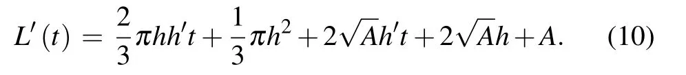
Doping concentration and thickness of an epitaxy layer are the two most essential parameters for any type of power devices. They should be determined at the initial step of device designs. An accurate extraction of epitaxy layer parameters lays the basis for any further analysis for finished devices.There are several methods to measure the doping profile of semiconductor materials,such as the capacitance-voltage(C–V),the spreading resistance,the Hall effect,the secondary ion mass spectroscopy (SIMS), and the Rutherford back scattering (RBS).[1]Among all the methods, the C–V method is a pure electrical non-destructive method with almost universal applicability.[2–9]The doping profile along the depth is obtained based on the relationship among the reverse voltage bias,the depletion depth,and the device capacitance by treating the device as a parallel-planar junction.[10]On account of the fact that the real power device has terminations,such a relationship may deviate from the parallel-planar junction and cause calculation errors of the doping profile. Among different kinds of terminations, the field limited ring (FLR) termination is one of the most commonly used terminations for its robustness and compatibility with the process.[11,12]The doping concentration will be overestimated and the thickness underestimated for devices with FLR terminations. The higher the voltage rate or the lower the current rate of the device,the higher the area ratio of occupation by the termination region,and the higher the calculation error. Such a phenomenon has yet not been addressed in literature. Although the effect of the depletion region lateral extension on the C–V characteristics and the corresponding doping profile calculation have been discussed before,[13,14]it is about the diffused junction and does not concern the termination. The shape of the depletion region at the device edge is assumed to be a cylinder.This assumption means that the vertical depth and the lateral width is considered to be equal, which is biased and not adequate for power devices with thick epitaxy layers and large FLR terminations.
In order to overcome the aforementioned difficulties, a new algorithm is proposed in this paper, which is based on C–V characteristics and the extension manner of the depletion region on the reverse bias, and is able to extract with higher accuracy of the epitaxy layer parameters of devices with uniformly doped epitaxy layers and FLR terminations.The extension manner of the depletion region on the reverse bias,especially the one under the FLR termination,features prominently in our new algorithm,meanwhile it depends on the design parameters of the FLR termination. Our new algorithm gives not only the epitaxy parameters but also the relationship between the horizontal extension width and the vertical depth of the depletion region under the FLR termination,which reveals the quality of the termination design.
Table 1. Notation of this paper.
This paper is a theoretical research based on experiments,and is arranged as follows. In Section 2,the conventional C–V method is briefly introduced and applied to simulated C–V characteristics to demonstrate its drawbacks. In Section 3,the new algorithm is established. Firstly, the extension manner of the depletion region is studied by simulation and modeling. The analytical expressions of the C–V characteristics and the effective doping profile are derived. The direct proportion relationship between the horizontal extension width and the vertical depth of the depletion region under the FLR terminations is proved by simulation. Then,the accurate values of the epitaxy layer parameters are acquired by fitting the effective doping profile analytical expression to the C–V doping profile calculated from the C–V characteristics. The direct proportion coefficient between the horizontal extension width and the vertical depth of the depletion region is also acquired. The credibility of our new algorithm is verified by applying it to the measured C–V characteristics of real devices. Finally,we discuss about the application of our new algorithm to FLR/field plate combining terminations. Section 4 concludes this paper. Our new algorithm can be used for the examination of deviation of the epitaxy layer parameters,the evaluation of the termination efficiency, and as the foundation for any further analysis and improvements.
2. The conventional algorithm and its drawbacks
First,we briefly introduce the conventional algorithm for extracting the epitaxy layer parameters. A parallel-planar Schottky junction is used as an example,as shown in Fig.1(a).Assume that the effective junction area is Aeff,the reverse voltage bias is VR, the depletion region depth is t, and the device capacitance is C. The word“effective”will be explained later.Suppose that VRincreases by dVR,then t increases by dt and the stored charge on the device capacitance increases by dQ.We have

Thus,
The C depends on t as
Substituting the above equation into Eq.(2),we finally obtain
and

Equation(4)gives the doping profile of the device, as shown in Fig.1(c).

Fig.1. The basic steps of the conventional algorithm for extracting the epitaxy layer parameters. The parallel-planar Schottky junction is used as an example. (a)When the effective junction area is Aeff,the reverse voltage bias is VR,the depletion region depth is t,and the local doping concentration is N(t). (b)The relationships among the device capacitance C,t, and VR. Here t is calculated by Eq.(3). (c)The C–V doping profile along the depth calculated by the conventional algorithm from the C–V characteristics.

Fig.2. (a)The structure and parameters of the SiC JBS diode used for C–V simulation. The partial C–V characteristics of the active part,the side part,and the corner part are simulated separately. (b)The simulated partial C–V characteristics of the active part,the four side parts,and the four corner parts,the sum of which is the total C–V characteristic. (c)The doping profiles calculated by the conventional algorithm. The black line is calculated from the active part C–V characteristic and the red line from the total C–V characteristic. The dashed line shows the actual doping profile set in the simulation.
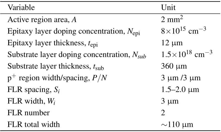
Table 2. The parameters of the device structure shown in Fig.2(a)used for simulation.
Since it is calculated from the C–V characteristics, we call it the C–V doping profile. When the depletion region extends to the epitaxy/substrate interface,the device capacitance C achieves its minimum value and stays unchanged. Thus,the doping profile bends upwards quickly and approaches infinity.The upward point can be viewed as the epitaxy layer thickness.
In order to check the accuracy of the conventional algorithm, we apply it to the simulated C–V characteristics of a SiC JBS diode with an FLR termination, whose structure is shown in Fig.2(a)and parameters in Table 2.
The partial C–V characteristics of the active part,the four side parts,and the four corner parts of this JBS diode are simulated separately by TCAD software Silvaco. The total C–V characteristic of the whole device is the sum of all these partial C–V characteristics. The results are shown in Fig.2(b).The C–V doping profiles calculated by the conventional algorithm are shown in Fig.2(c). The black line is calculated from the active part C–V characteristic. The doping concentration/thickness can be read as 8×1015cm−3/11.5µm,which is very close to the setting value in the simulation. The ∼0.5µm difference of the thickness is caused by the p+/n junction depth. The red line is calculated from the total C–V characteristic of the whole device. Such a doping profile shows an increasing trend as the depth increases, and the epitaxy layer thickness is only 9.5 µm, which is far less than the setting value. These results clearly show that the conventional algorithm tends to overestimate the doping concentration and underestimate its thickness.

3. The establishment of the new algorithm
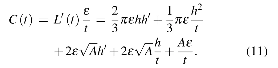
In this section, the new algorithm is established step by step.The schematic diagram of this new algorithm is shown in Fig.3. Firstly,the extension manner of the depletion region is studied by simulation and modeling. Based on this extension manner, the analytical expressions of the C–V characteristics and the effective doping profile are derived. Concurrently,the C–V doping profile of the device under test is calculated by the conventional algorithm from its C–V characteristics. The doping concentration Nepi,the epitaxy layer thickness tepi,and the horizontal extension coefficient k are acquired by fitting the effective doping profile analytical expression to the C–V doping profile. The details are explained in the following parts.
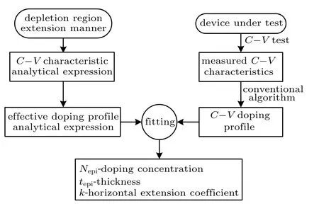
Fig.3. The schematic diagram of the new algorithm.
3.1. The extension manner of the depletion region under the FLR termination
The device capacitance is determined by the depletion region, and the depletion region is determined by the reverse voltage bias. In order to study the relationship between the shape/size of the depletion region and the reverse voltage bias,the boundaries of the depletion regions at different reverse biases under the FLR terminations with varied and equal ring spacing values are overlapped,as shown in Figs.4(a)and 4(b),respectively. The FLR termination in Fig.4(a)is the same as that of the device in Fig.2(a), with ring spacing values increasing from 1.5 µm at the innermost ring to 2.0 µm at the outermost ring. The FLR termination in Fig.4(b) has equal ring spacing values of 1.5µm. It can be observed that all these boundaries are similar to straight lines for either varied ring spacing or equal ring spacing FLR terminations.
We still represent the vertical depth of the depletion region under the active region as t and the horizontal width in the FLR termination as h. Here h increases as t increases and they satisfy a one-to-one function relationship h=h(t). The concrete form of h(t)will be discussed in Subsection 3.3.
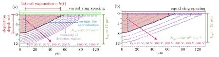
Fig.4. The boundaries of the depletion regions under the FLR terminations: (a)varied ring spacing(the same FLR design as that of the device shown in Fig.2(a));(b)equal ring spacing. These boundaries at different reverse biases all appear similar to straight lines.
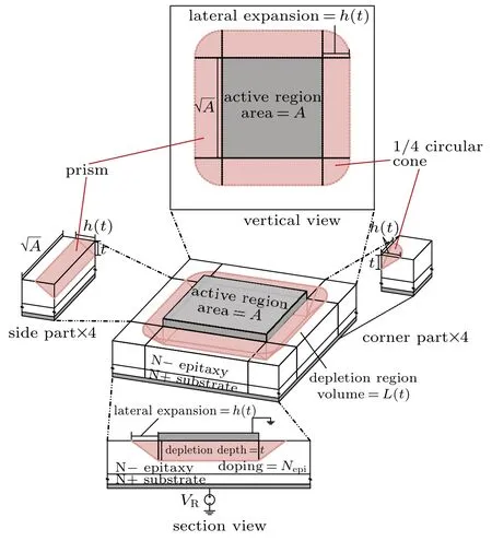
Fig.5. The shape of the depletion region can be approximated by the combination of simple geometric bodies: one cuboid,four prisms,and four 1/4 circular cones.
Considering the straight-line approximation discussed above,the shape of the depletion region can be approximated by the combination of simple geometric bodies, as shown in Fig.5. The active region of the device can be seen as a square(area=A) with the four fillets ignored. The depletion region depth t under the active region satisfies

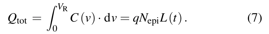
The charge Qtotstored in the device capacitance satisfies
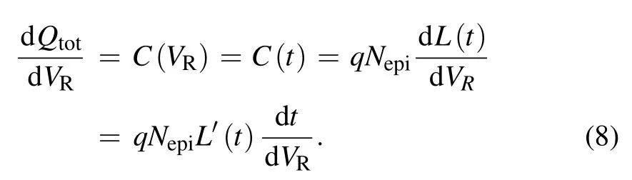
Qtotdepends on VRas well as t. Take the derivative of the above equation with respect to VR,we have
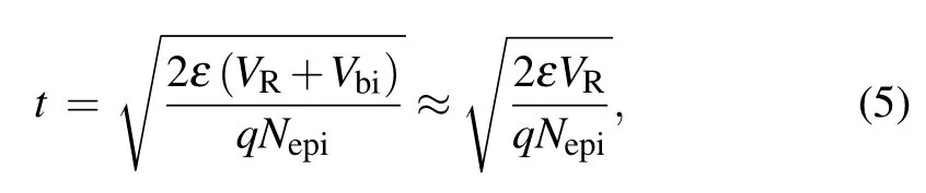
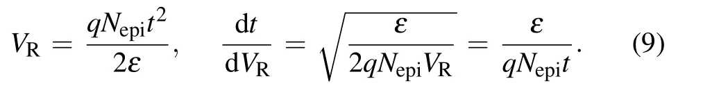
According to Eq.(5)we have(with Vbiignored)
According to Eq.(6)we have
Thus,Eq.(8)changes to
Therefore,we acquired the relationship between the device capacitance C and the depletion region depth t.
3.2. The analytical expression of the effective doping profile
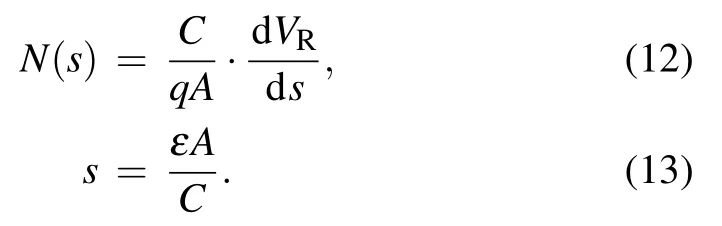
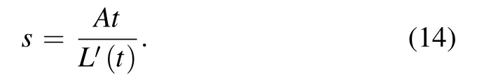
Based on the derivation results in Section 3.1,the analytical expression of the effective doping profile is derived in this part. As mentioned in Section 2, when we assume Aeff=A,Eq. (4a) gives the effective doping profile N(s) and Eq. (4b)the effective depth s. Thus,we have
Substituting Eq.(11)into Eq.(13),we have
Hence,

Substituting Eqs.(11)and(15)into Eq.(12),we have

where
Equation(16)is the analytical expression of the effective doping profile. It is expressed by the active region area A, the actual doping concentration Nepi,and the depletion region horizontal extension width h. Thus,it contains the information of the epitaxy layer of the real device and depletion region extension manner under the FLR termination. Since it does not contain the C–V information anymore,we call it the“(analytically expressed) effective doping profile” in order to distinguish it from the calculation given by Eq.(4).
3.3. The direct proportion relationship between the vertical depth t and the horizontal width h
In order to acquire an explicit expression of the effective doping profile (Eq. (16)), the function h(t) should be determined. According to Eqs. (10) and (17), the first and second derivatives of the depletion region volume L(t)have very complicated forms. The following calculations would be cumbersome if h(t) cannot acquire a simple form. Fortunately, it is noticed in Fig.4 that the boundaries of the depletion regions at different reverse voltage biases are nearly parallel to each other,i.e.,the horizontal width h seems to be directly proportional to the vertical depth t. We donate this relationship as h(t) = kt,in which k is the horizontal extension coefficient.
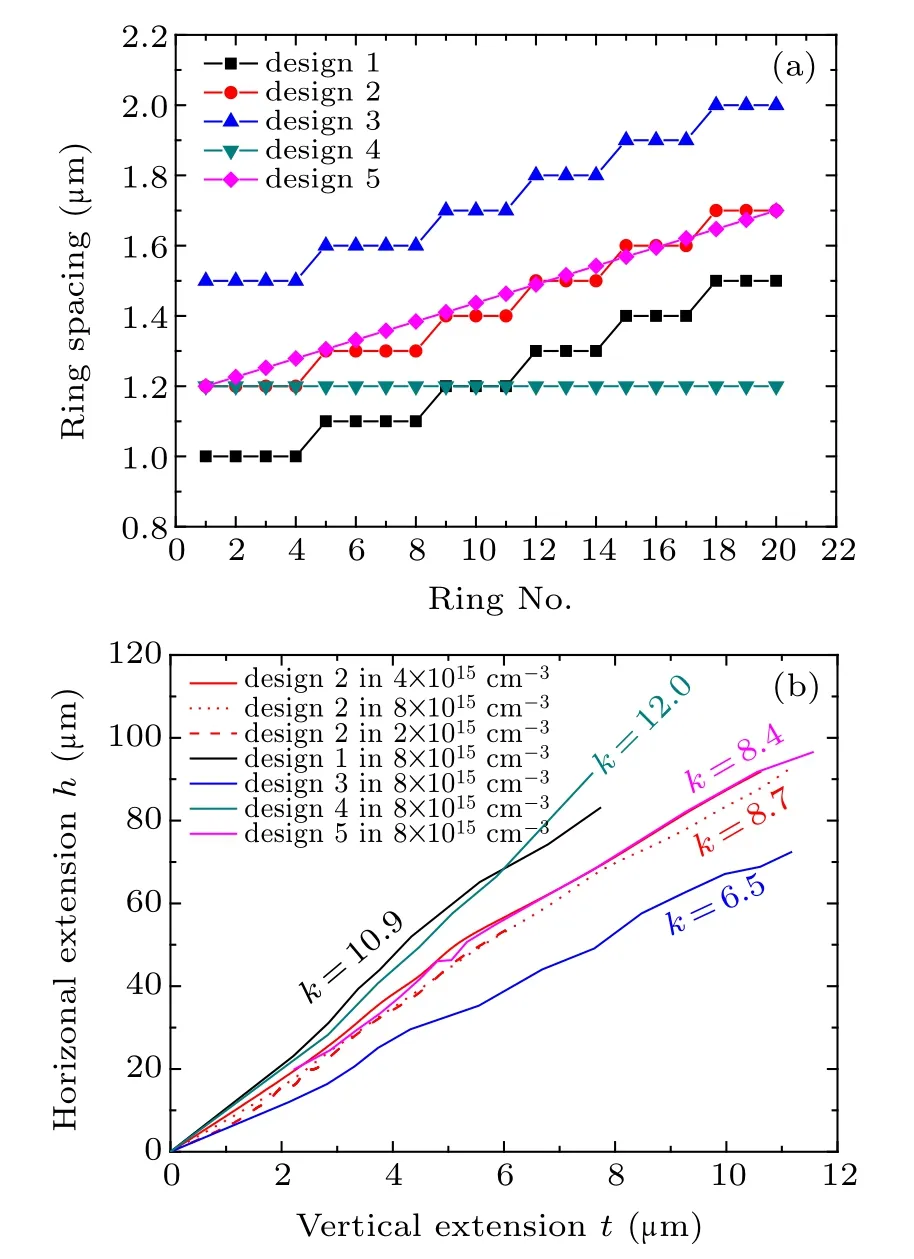
Fig.6. (a)The ring spacing values of different FLR terminations used in the simulation. The ring width is fixed at 3µm. (b)The approximate direct proportion relationship of the horizontal width h and the vertical depth t of different FLR structures in different epitaxy layers.
In order to verify this observed result more sufficiently,simulations are performed on FLR terminations with different ring spacing values and epitaxy layer parameters. Figure 6(a)shows the ring spacing values used in the simulation,and Fig.6(b)shows the relationships between h and t. It can be seen that h and t approximately satisfy the direct proportion relationship for different FLR structures and epitaxy layer parameters. Moreover,the direct proportion coefficient k can be used as an index for the design quality of FLR terminations.An FLR termination with a low k value has higher efficiency since it demands a smaller area of the device.

The device capacitance(Eq.(11))changes to

Expressing the above equation with the independent variable VR,we have

It is easy to distinguish the three terms of the above equation for the partial capacitance of the four corner parts,the four side parts, and the active part, respectively. Equation (14), which links the actual and effective depletion region depths(t and s),changes to

Arrange the above equation while regarding t as the unknown variable,we have

One root of this quadratic equation is
where

Actually, Eq. (22) has two roots. We only take the smaller one, and the reason is explained in Appendix A.Substituting Eqs.(18)and(23)into Eq.(16),we have

The above equation is simplified to the analytical expression of the effective doping profile.The maximum values of the actual and effective depletion region depths (tepiand smax) also satisfy Eq.(23),hence
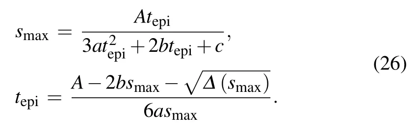

Fig.7. (a)The calculated(by Eq.(20))and simulated C–V characteristics of the device shown in Fig.2(a). The built-in voltage Vbi is extracted as 1.6 V.C–V curves with zero Vbi are also shown for comparison. (b)The effective profile calculated by Eq.(25)and the C–V doping profile calculated by the conventional algorithm(i.e.,the doping profile shown in Fig.2(c)).

Fig.8.The calculated total C–V characteristics(by Eq.(20))and the effective doping profiles(by Eq.(25))with different doping concentrations(Nepi)and horizontal extension coefficients(k)of the real device. The active region area A and the built-in potential Vbi is fixed at 2 mm2 and 1.6 V,respectively. (a)and(b)Nepi fixed at 8×1015 cm−3 and k varies;(c)and(d)k fixed at 5 and Nepi varies.
We now use the device in Fig.2(a) as an example to demonstrate the rationality of the above derivation. According to the results in Fig.6(b), we have k = 6.5. The partial and total C–V characteristics can be calculated by Eq. (20), where the built-in potential Vbi(=1.6 V)is extracted from the simulated 1/C2–V curve.[1]The calculated C–V curves are quite close to the simulated ones,as shown in Fig.7(a). The calculated C–V curves with zero Vbiare also shown for comparison,and it can be seen that Vbionly affects the low VRpart of the C–V curves.The effective doping profile can be calculated by Eq.(25),and its effective epitaxy layer thickness by Eq. (26). The calculated effective doping profile is quite close to the C–V doping profile obtained by the conventional algorithm, as shown in Fig.7(b). Hence,the rationality of the aforementioned derivation has been verified.
A more detailed study about the total C–V characteristics and the effective doping profiles is stated as follows. The active region area A is fixed at 2 mm2as before.When the epitaxy layer concentration Nepiis fixed at 8×1015cm−3and the horizontal extension coefficient k varies,the total C–V characteristics calculated by Eq. (20) and the effective doping profiles calculated by Eq. (25) are shown in Figs. 8(a) and 8(b),respectively. Similarly, when k is fixed at 5 and Nepivaries,the corresponding C–V characteristics and the effective doping profiles are shown in Figs.8(c)and 8(d),respectively. The upward points of the effective doping profiles, i.e., the effective epitaxy layer thickness,are calculated by Eq.(26).
As shown in Fig.8(c), the total device capacitance increases as Nepiincreases,since the depletion region depth decreases. Comparatively, as shown in Fig.8(a), where Nepiis fixed, the effective doping profile keeps almost unchanged despite a large variation of k. On the contrary, as shown in Fig.8(b), the effective doping profile shows an obvious variation. In other words, the slight differences in the C–V characteristics are magnified during the calculation for the C–V doping profiles. Figure 8(b)also shows that the effective doping profile is always an increasing function of the effective depletion region depth s. With Nepifixed, the larger the k is,the more obvious the increasing trend is, and the smaller the epitaxy layer thickness is. Contrarily, as shown in Fig.8(d),where k is fixed, Nepihas no effect on the increasing trend of the effective doping profiles. In other words, the severer the extension of the depletion region under the FLR termination,the larger its influence on the device capacitance,and the severer the overestimation and underestimation by the conventional algorithm of the doping concentration and thickness,respectively.
3.4. Extraction of the epitaxy layer parameters

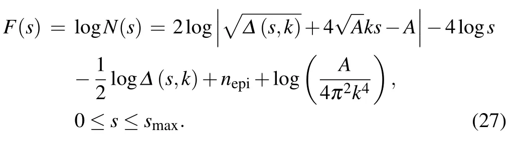
Suppose that the logarithm of the C–V doping profile calculated from the measured C–V characteristics is G(s),our target is to adjust the parameters k and nepito minimize the distance between the two functions F(s)and G(s). The 2-norm can be used as a measure of the function distance:
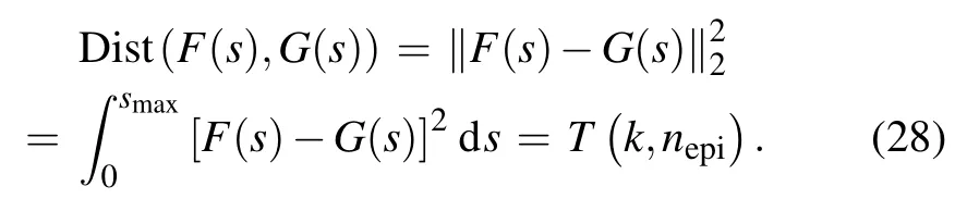
On the right side of the last equal sign of the above equation,the function distance is regarded as a two-variable function T of k and nepi. Hence,our target changes to find the minimum point of the function T. Considering the complicated expression of the function T, the gradient descent method can be used here. The expressions of the gradient of the function T are shown in Appendix B.As long as the minimum point(k0,nepi,0) is determined, the epitaxy layer doping concentration and thickness can be calculated as

The following two examples are used to verify our new algorithm. We choose two SiC diodes with FLR terminations:one is our self-fabricated 1200 V/2 A MPS diode(our diode),and the other is a 1200 V/5 A JBS diode (serial number:C4D05120A)purchased from CREE(CREE diode). The parameters of these two diodes are listed in Table 3. The actual values of the doping concentration and thickness of our diode are offered by the epitaxy wafer manufacture.

Table 3. The parameters of our diode and CREE diode.
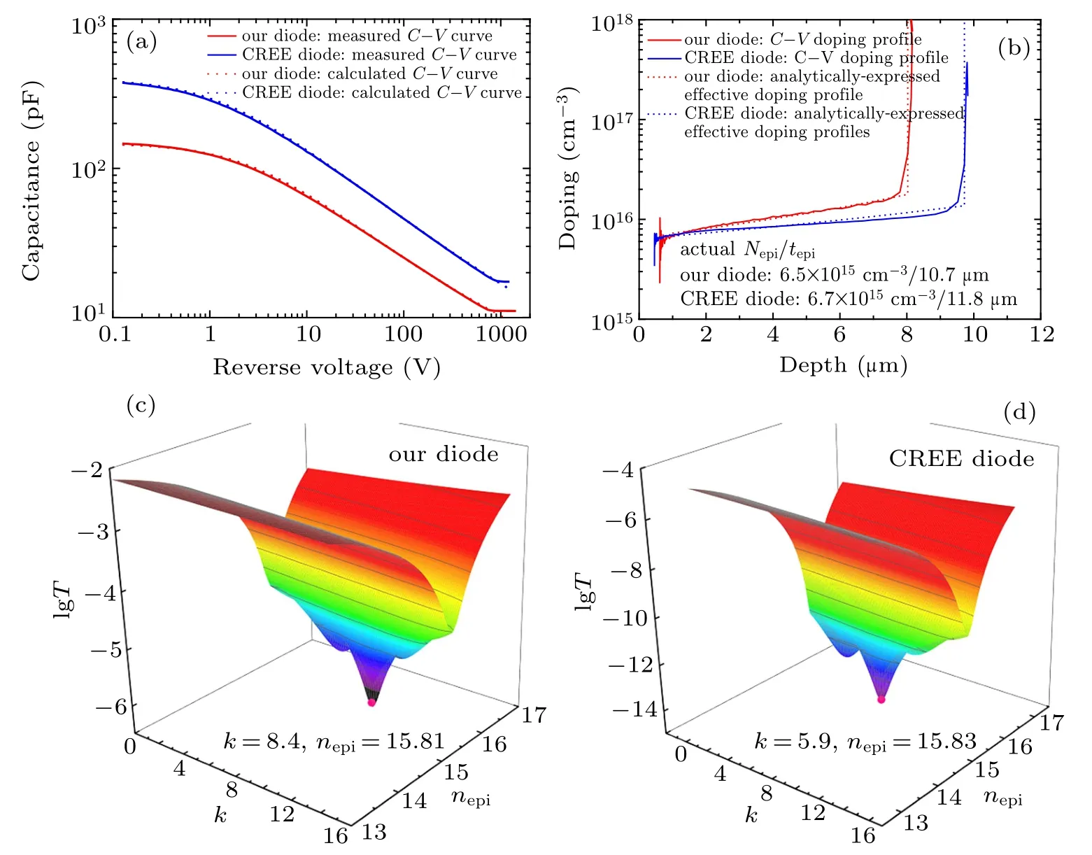
Fig.9. (a)The measured C–V characteristics of our diode and CREE diode,as well as the calculated ones by Eq.(20)with the fitted parameters(k,nepi)obtained by our new algorithm. (b)The C–V doping profiles(Eq.4))calculated by the conventional algorithm from the measured C–V characteristics,as well as the analytically expressed effective profiles calculated by Eq.(25)with the fitted(k,nepi).The extracted actual doping profiles are also shown. (c)and(d)The surfaces of the function T and their minimum points of our diode and CREE diode,respectively.

Fig.10. (a)The measured C–V characteristics of our self-made 19 diodes and their(b)C–V doping profiles(Eq.(4)). The bar charts of(c)the extracted epitaxy layer doping concentrations and(d)thickness of the 19 diodes,as well as their relative errors with respect to the actual values.
In order to provide a statistical study of our new algorithm, we have measured the C–V characteristics of a batch of our self-made 1200 V/2 A SiC diodes (19 diodes in total fabricated on the same wafer,including the one mentioned in Fig.9),as shown in Fig.10(a). The C–V doping profiles calculated by the conventional algorithm are shown in Fig.10(b).We apply our new algorithm to these 19 diodes and the extracted epitaxy layer doping concentration and thickness values are shown in Figs.10(c)and 10(d),respectively,as well as the relative errors with respect to the actual values. The relative error is calculated as the extracted value minus the actual value and then divided by the actual value. The extracted doping concentrations lay in the range of(6.4±0.24)×1015cm−3,and the relative error is less than ±4%. The extracted thicknesses lay in the range of(10.4±0.4)µm,and the relative error is also less than±4%.The above results in Figs.9 and 10 have verified the accuracy of our new algorithm.
3.5. Application of the new algorithm to FLR terminations with field plates
Sometimes, FLR terminations are combined with field plates to relieve the high-electrical field at the innermost rings.The structural diagram of an FLR termination with a metal field plate is shown in Fig.11(a). The situation of a polysilicon field plate is similar. The field plate often only covers the innermost several rings.
We still use the simulation to study the extension manner of the depletion region under the FLR termination with a field plate. The FLR structure is the same as that in Fig.2(a),plus with a field plate. The field plate length is set at 0 µm,5 µm, 10 µm, and 20 µm. Figure 12 shows the depletion region boundaries of different field plate lengths and at the same reverse biases. The depletion region boundaries under the field plates almost coincide with each other,while outside the field plates they are approximately parallel to each other.In other words,the field plate does not affect the vertical depth of the depletion region,but only shifts it outwards. Figure 13 proves again this fact, in which the relationships of the horizontal width h and the vertical depth t of FLRs with different field plate lengths are shown. The h–t lines according to different field plate lengths are almost parallel with each other,but only with different intercepts at the h-axis. The intercepts at the h-axis are approximately their field plate lengths.
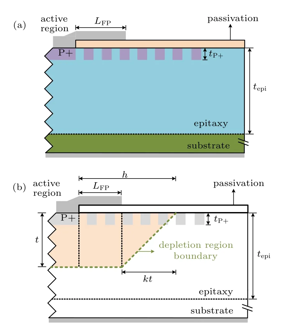
Fig.11. (a)The structural diagram of an FLR termination with a field plate. (b) The shape the depletion region under the FLR termination with a field plate.
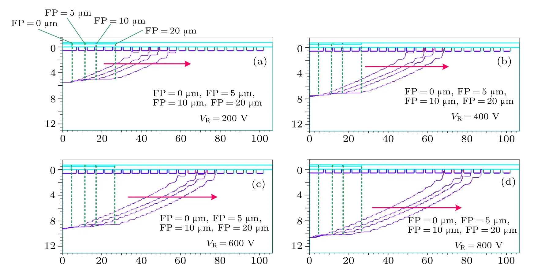
Fig.12. The boundaries of the depletion regions under FLR terminations with field plates of different lengths(0µm,5µm,10µm,and 20µm)and at the same reverse biases(200 V,400 V,600 V,800 V).
This equation has the same form as Eq.(18), and the following calculation is similar. The device capacitance can still be expressed as Eq.(19),and the analytical expression of the effective doping profile can still be expressed as Eq. (25). The different point is that the capacitance of the active part, the side parts, and the corner parts are not simply expressed by the negative-one-order, the one-order, and the constant terms of Eq.(19),but calculated as

In order to demonstrate the rationality of the above derivation,we use the device structure shown in Fig.2(a),plus with a 20µm-long field plate to simulate theC–V characteristics.According to the results in Fig.13,we have k = 6.57.The partial and total C–V characteristics can be calculated by Eqs. (35),(36), (37), and (19). The built-in potential Vbiis extracted as 1.72 V.The calculated C–V curves are quite close to the simulated ones,as shown in Fig.14(a).The effective doping profile can be calculated by Eq.(25). The calculated effective doping profile is quite close to the C–V doping profile obtained by the conventional algorithm, as shown in Fig.14(b). Hence, the rationality of the aforementioned derivation has been verified.
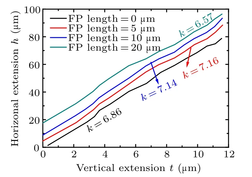
Fig.13.The relationship of the horizontal width h and the vertical depth t of FLRs with different field plate lengths.
The fitting process to extract the epitaxy layer parameters from the analytically expressed effective profile is similar to that shown in Section 3.4. The difference is that the distance between the two functions F(s) and G(s) is a three-variable function T of k,nepi,and LFP(refer to Eq.(28)),i.e.,

The gradient descent method can still be used here to find the minimum point (k0, nepi,0, LFP0). In summary, our new algorithm can still be applied to devices with FLR/field plate combined terminations. The expressions of the device capacitance and the analytical expressed effective doping profile are similar to those of simple FLR terminations. The difference is that their coefficients are slightly modified,with the field plate length(LFP)included.

Fig.14. (a)The calculated and simulated C–V characteristics of the device shown in Fig.2(a),plus with a 20µm-long field plate. The built-in voltage Vbi is extracted as 1.72 V.(b)The effective profile and the C–V doping profile calculated by the conventional algorithm.
4. Conclusion
A new algorithm for accurate extraction of the epitaxy layer doping concentration and thickness of power devices with uniform doped epitaxy layers and FLR terminations is proposed in this paper,with a motivation to overcome the inaccuracy of the conventional algorithm caused by the ignorance of the influence of the terminations. This new algorithm is based on the C–V characteristics and the extension manner of the depletion region on the reverse bias. The depletion region extension under the FLR terminations, which depends on the epitaxy layer parameters and FLR termination designs,is studied in detail by simulation and modeling. The direct proportion relationship between the horizontal extension width and the vertical depth of the depletion region under the FLR terminations is proved by simulation. Analytical expressions of the C–V characteristics and the effective doping profile are derived, by which the reason for the overestimation and underestimation of the doping concentration and thickness,respectively,by the conventional algorithm,is explained. The actual doping concentration and thickness can be obtained by fitting the analytically expressed effective doping profile to the C–V doping profile acquired by the conventional algorithm. The horizontal extension coefficient of the depletion region is also given, which can be used as an index for the design quality of FLR terminations. The credibility of our new algorithm is verified by simulations and experiments. Our new algorithm,with only necessary but slight modifications,is also applicable to FLR/field plate combining terminations.The new algorithm proposed in this paper furnishes us with a non-destructive and accurate method to obtain epitaxy layer parameters of finished devices. It can be used for the inspection of the wafer parameters on which devices are fabricated, for the initial steps of the reverse engineering on unknown devices, and lay a solid foundation for further analyses and improvements.
Acknowledgment
The authors (Jiupeng Wu, Na Ren, and Kuang Sheng)thank the Technology Innovation and Training Center, Polytechnic Institute, Zhejiang University, Hangzhou, China for providing the Agilent B1505A curve tracer and MPI probe station.
Appendix A
We have mentioned in Section 3.3 that we only take the smaller root of Eq. (22). The reason is explained as follows. The device shown in Fig.2(a) (Nepi/tepi= 8×1015cm−3/12 µm, k=6.5) is used as an example. The partial and total capacitance of the device can be calculated by Eq.(19),and the relationship between s and t can be calculated by Eq.(21),as shown in Figs.A1(a)and A1(b),respectively.As t increases, the capacitance of the corner parts becomes larger and larger and finally dominates in the total capacitance.Therefore, the total capacitance firstly decreases and then increases as t increases. Combining Eqs.(19)and(21),we have

As the left side of the above equation(i.e.,the device total capacitance) firstly decreases and then increases, s should firstly increase and then decreases. This is the reason why one s has two corresponding t values in Fig.A1(b). From Fig.A1(a) it can be noticed that the corner part capacitance dominates only when t>164µm. However,the epitaxy layer of the real device has a limited thickness, and there is no enough space for the extension of the depletion region. Thus,the range of t is restricted within 0–164 µm. Consequently,only the first half part of the s–t curve is allowed in Fig.A1(b),and thus one s corresponds to only the smaller t.

Fig.A1. With the parameters of the device shown in Fig.2(a)(Nepi/tepi = 8×1015 cm−3/12µm,k = 6.5),(a)the partial and total capacitance calculated by Eq.(19),and(b)the relationship between the actual and effective depletion region depths s and t calculated by Eq.(21).
Appendix B


where

with

猜你喜欢
广东省社会主义学院学报(2022年4期)2023-01-19
——全省各级审计机关集中收听收看党的二十大开幕盛况
审计与理财(2022年10期)2022-11-11
生活用纸(2022年10期)2022-10-11
湖南大众传媒职业技术学院学报(2022年4期)2022-02-19
Chinese Physics B(2021年9期)2021-09-28
作文大王·低年级(2021年2期)2021-02-21
新民周刊(2017年41期)2017-11-03
美与时代·美术学刊(2016年8期)2016-11-09
浙江工商职业技术学院学报(2016年2期)2016-01-22
创意城市学刊(2015年3期)2015-02-27

- Chinese Physics B的其它文章
- Speeding up generation of photon Fock state in a superconducting circuit via counterdiabatic driving∗
- Micro-scale photon source in a hybrid cQED system∗
- Quantum plasmon enhanced nonlinear wave mixing in graphene nanoflakes∗
- Restricted Boltzmann machine: Recent advances and mean-field theory*
- Nodal superconducting gap in LiFeP revealed by NMR:Contrast with LiFeAs*
- Origin of itinerant ferromagnetism in two-dimensional Fe3GeTe2∗