
Optical simulation of CsPbI3/TOPCon tandem solar cells with advanced light management
2022-08-31 09:55MinYue岳敏YanWang王燕HuiLiLiang梁会力andZengXiaMei梅增霞
Chinese Physics B 2022年8期
关键词:王燕
Min Yue(岳敏) Yan Wang(王燕) Hui-Li Liang(梁会力) and Zeng-Xia Mei(梅增霞)
1Beijing National Laboratory for Condensed Matter Physics,Institute of Physics,Chinese Academy of Sciences,Beijing 100190,China
2Songshan Lake Materials Laboratory,Dongguan 523808,China
3School of Physical Sciences,University of Chinese Academy of Sciences,Beijing 100049,China
Keywords: perovskite/Si tandem solar cells,simulation,TOPCon,CsPbI3
1. Introduction
Crystalline silicon (c-Si) solar cells have occupied over 90% photovoltaic market due to their low cost, high efficiency and mature industrialization. The power conversion efficiency(PCE)of current world record cell for single-junction c-Si solar cells is 26.7% which is close to the 29.4% efficiency limit of Si.[1,2]In order to break through this efficiency ceiling,one approach is to fabricate multi-junction solar cells which can effectively enhance the utilization of the solar spectrum by reducing the thermalization loss. The theoretical efficiency of Si based two-junction solar cells can exceed 45% which is quite attractive.[3]The calculation result manifests that Si (Eg=1.12 eV) based TSC requires an absorption material withEg∼1.70 eV in the top cell so as to maximize the efficiency.[3]Halide perovskites with tunable bandgap(1.5 eV–2.3 eV),high absorption coefficient and good defect tolerance,[4,5]have rapidly enhanced the PCE from 3.8% to 25.7% in the last ten years.[6,7]The bandgap of perovskite can be ideally adjusted to 1.67 eV–1.75 eV by changing the composition of ABX3.[8]
It is quite incredible that the PCE of perovskite/Si(PVK/Si)TSCs has developed extremely fast, from 13.7%in 2015[9]to 29.8% in 2021,[10]exceeding that of the c-Si solar cells. In high-efficiency PVK/Si TSCs,silicon heterojunction (SHJ) solar cell is usually chosen as the bottom cell because of its high PCE and high open-circuit voltage(Voc).[11]However, the SHJ totally distinguishes from the mainstream passivated emitter and rear cell (PERC), leading to a quite high levelized cost of electricity (LCOE). The tunnel oxide passivated contact(TOPCon)silicon solar cell is another outstanding candidate for the bottom Si solar cell which is compatible better with existing PERC production lines and has manifested a high record efficiency of 26.0%.[12]The LCOE of PVK/TOPCon TSCs has been calculated to be lower than PVK/SHJ TSCs for both utility and residential installation by Fraunhofer ISE.[13]Currently,the researches of PVK/Si TSCs mainly focus on organic-inorganic hybrid perovskite due to its relatively high efficiency. However, its thermal stability is still a huge challenge.[14]On the other hand,the all inorganic perovskite CsPbI3has been demonstrated to be more superior thermal stability and incredibly increased PCE from 2.9% to 20.37% in 6 years.[15,16]Meanwhile, the optimal bandgap of CsPbI3is 1.72 eV,[17]which is suitable for the application of PVK/Si TSCs.
To further improve the PCE of PVK/Si TSCs,one effective way is to reduce optical loss by employing light trapping structures. Upright pyramid structure is the most common texture in silicon solar cells, and achieved by etching silicon wafer in a mixed alkali solution.[18]In the PVK/Si TSCs,the upright pyramid structure is usually employed in rear side of silicon solar cell while the front side is polished because of the difficulty in obtaining uniform perovskite film by spin coating on textured surface.[19,20]However, the front planar surface of silicon results in poor light tapping capability. In order to cope with this challenge, upright pyramidal polydimethylsiloxane (PDMS) structure has been introduced on the top of TSCs.[21]Micrometer-thick perovskite top cell was spincoated on fully upright pyramidal textured silicon solar cell to avoid shunt paths.[20]Double-side-textured silicon cell with sub-micrometer pyramids was employed in order to minimize the thickness of perovskite film by solution process.[22]Furthermore, the inverted pyramid structure was proposed as a more promising texture, which has a lower reflectivity than upright pyramid.[23,24]It was introduced into the PVK/Si TSC by adding an inverted pyramidal PDMS antireflective coating, which would complicate the fabrication process.[25]Directly texturing on Si seems a more practical approach to mass production.[26]Nevertheless,such a research is still relatively limited,and more attention should be paid to realizing the application of such an excellent texture to PVK/Si TSC.
Herein, we design the optics of CsPbI3/TOPCon TSCs based on optical simulation that combines transfer matrix method(TMM)with ray-tracing method.The optical losses of different surface structures of silicon bottom solar cells such as rear-side upright pyramid(r-UP),bifacial upright pyramid(b-UP), and bifacial inverted pyramid (b-IP), are systematically discussed. In order to further optimize the surface structure of silicon, the dependence of optical loss on the bottom angle of rear-side b-IP is investigated particularly. Meanwhile,the photogenerated current densities of TSCs are calculated by varying the thickness of CsPbI3layer and Si bulk considering the fact that the current density matching is a key issue in two-terminal TSCs. Moreover, through comparing the optical performances of various transparent conductive oxide(TCO)layers,we find the hydrogenated indium oxide(IO:H)a more attractive front TCO candidate. Finally, the PCE of the CsPbI3/TOPCon TSC can achieve 31.78% when the best matched current density is realized.
2. Device simulation parameters
The sketches of CsPbI3/TOPCon TSCs with various textures are shown in Fig. 1. The material, function, and thickness of each layer are listed in Table 1 (their refractive indexes and extinction coefficients can be found in Fig. S1 in Supporting information. Both upright pyramid and inverted pyramid are 2-µm wide with an angle of 54.7◦, consistent with our previous experimental data.[23]As the thickness of SiOxlayer is extremely thin (∼1.5 nm), its influence can be reasonably ignored during the optical simulation. The rear and front ITO electrodes possess an identical carrier concentration of 2.0×1020cm−3in that too high carrier concentration will result in high free carrier absorption at long wavelengths. The interlayer ITO has a carrier concentration of 4.9×1020cm−3for the sake of favorable charge transfer between the subcells.[27]
Table 1. List of simulation parameters.
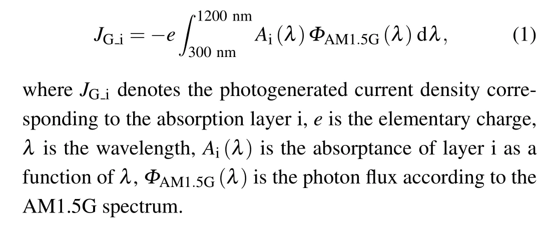
The optical properties of the CsPbI3/TOPCon TSCs were simulated by the widely used ray-tracing method and TMM for the Si thick layer and other thin layers,respectively.[35]The origin code of simulation can be acquired from website.[36]The normal incidence AM1.5G spectrum (from 300 nm to 1200 nm in steps of 10 nm) was chosen as the illuminant.In order to calculate the photogenerated current density, the internal quantum efficiency (IQE) was assumed to be 100%.Thus,the photogenerated current density could be determined by integrating the photon flux of the AM1.5G solar spectrum with the corresponding absorptance, expressed as the following equation:[32]
2.1. Textures

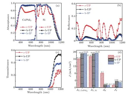
Fig.2. Optical properties of CsPbI3/TOPCon TSCs with three different textures,showing(a)absorptance of CsPbI3 layer and Si bulk,(b)reflectance of TSCs,(c)transmittance of TSCs,and(d)current densities of absorbed or lost lights(in units mA/cm2).
2.2. Bottom angle of rear-side inverted pyramid

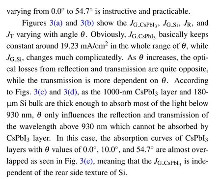

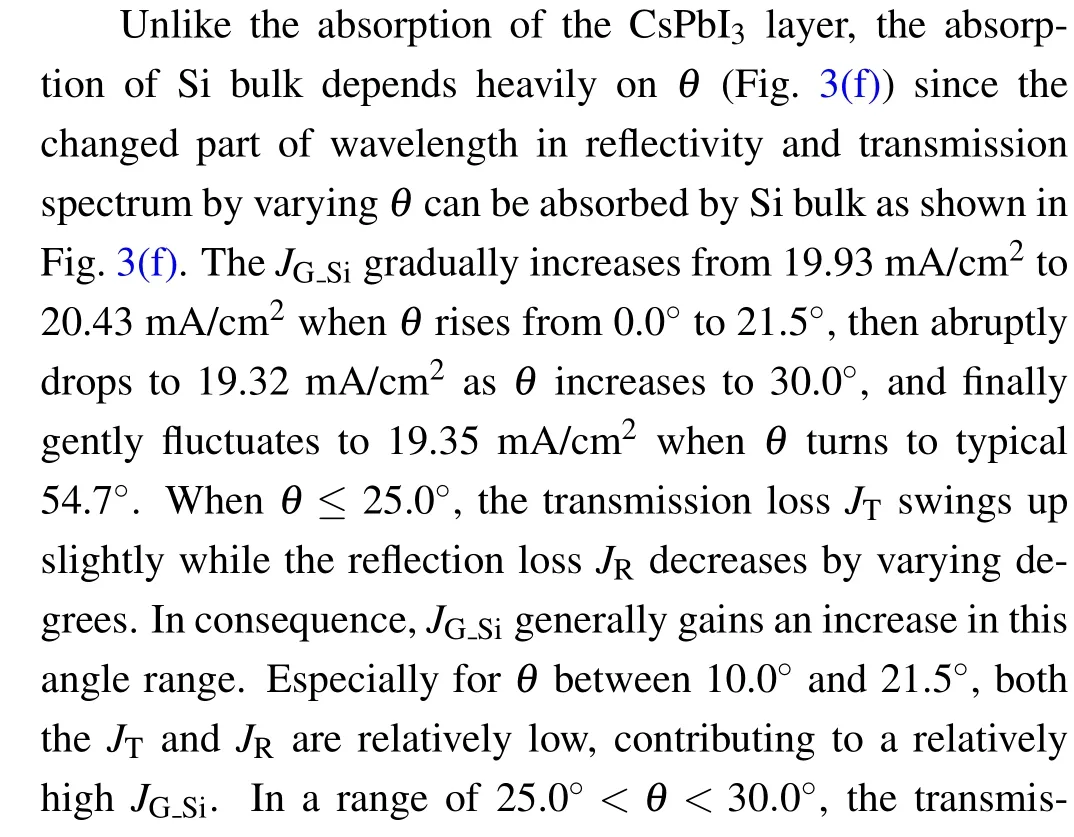
Fig. 3. (a) Photogenerated current density of CsPbI3 layer and Si bulk with respect to θ; (b) current density loss of TSC triggered by reflection and transmission versus θ; (c) wavelength-dependent reflectance, and (d) transmittance of TSC for different values of θ; absorptance of (e) CsPbI3 layer and(f)Si bulk for different values of θ.


wherenSiandαSiare the refractive index and incident angle of Si,njandαjare the refractive index and incident/refraction angle of the layer j between Si and air,n0andα0are the refractive index and refraction angle of the air, respectively. In other words, the incident angle in Si for the total internal reflection at the top or bottom interface of TSCs only depends onnSiandn0. Our previous work have illustrated that whenθ>4◦,the reflection in the front interface of TSCs will generally decrease with the increase ofθbecause of the enhanced probability of total internal reflection;whenθ<24◦,the transmission in the rear interface of TSC will be suppressed for the same reason.[39]Therefore,a smallθcan make a trade-off between reflection and transmission, contributing to a higherJGSi.Thus,in order to maximize the optical harvest in PVK/Si TSCs, the rear side texture should become smoother, which will be simultaneously benefciial to the passivation of the rearside surface of Si subcell.
2.3. Thickness of CsPbI3 layer and Si bulk
Current density matching between the top subcell and bottom subcell is one of the most critical issues in twoterminal TSCs.In order to maximize the series current density of the CsPbI3/TOPCon TSCs, the thickness value of CsPbI3layer and Si bulk should be delicately modulated to achieve a positive match. Asymmetrical b-IP with a bottom angle 10◦of rear-side was chosen for the texture of Si subcell in this subsection. The thickness of CsPbI3layer varies from 400 nm to 2200 nm in steps of 20 nm, while the Si bulk’s ranges from 40µm to 210µm in steps of 10µm.

Fig. 4. Simulated optical performances of CsPbI3/TOPCon TSCs with different values of thickness of CsPbI3 layer and Si bulk. (a) Photogenerated currentdensity of CsPbI3 layer; (b)JG CsPbI3 andJG Si,withSi bulk thickness fxiedat180µm; (c)absorption spectrum ofCsPbI3 layer andSi bulk,withthickness of Si bulk fxied at180µm butthicknessof CsPbI3 layer varied; (d)photogeneratedcurrent density ofSi bulk; (e)JGCsPbI3 and JGSi,withthickness of CsPbI3 layer fxied at 400 nm;(f)absorptionspectra of CsPbI3 layer andSibulk,with thickness of CsPbI3layer fxied at 400 nmbut thickness of Si bulk varied.
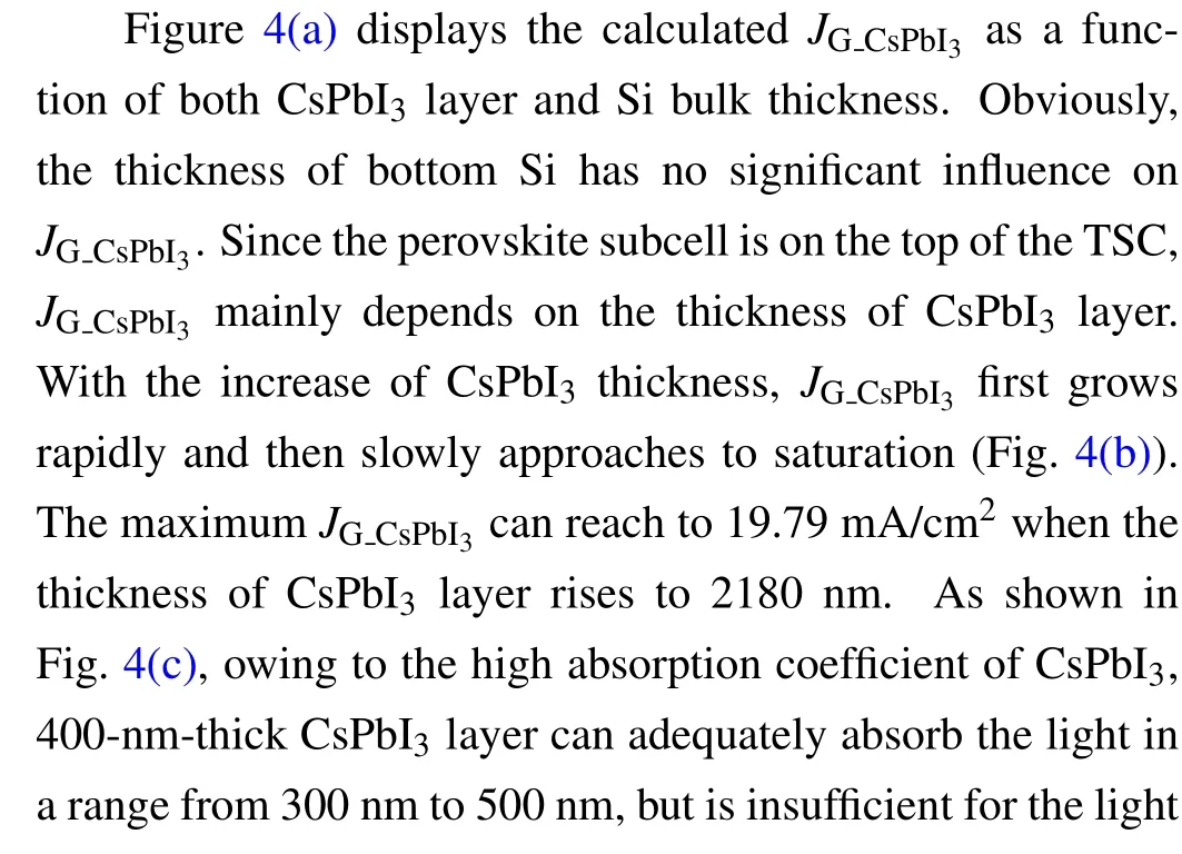

Basically, the short-circuit current density (Jsc) of the entire two-terminal TSC reaches up to the lower one of the two subcells, bringing out the key problem of current matching. Figure 5 exhibits theJscof CsPbI3/TOPCon TSCs and thickness of both CsPbI3layer and Si bulk for current density matching. When the CsPbI3layer is thinner than 600 nm,Jscis unilaterally restricted by theJGCsPbI3, indicating that even 40-µm Si is thick enough to match with CsPbI3layer. With the increase of CsPbI3layer thickness, the Si bulk should be thickened correspondingly. At present, the thickness of industrial used Czochralski (CZ) Si wafer is∼180 µm, which is absolutely thick enough to match with a 2000-nm CsPbI3layer. According to previously published experimental data,the thickness of CsPbI3layer is usually less than 1000 nm as a result of crystallization quality, implying that theJscof the CsPbI3/TOPCon TSC will be mainly determined by the thickness of CsPbI3layer. On the other hand, the bottom Si substrate has suffciient space to become thinner. The maximumJsccan reach to 19.79 mA/cm2when the thickness of Si bulk and CsPbI3layer are 180µm and 2180 nm,respectively.
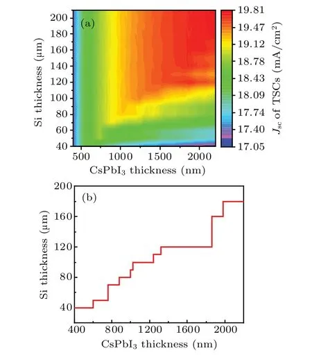
Fig. 5. (a) Short-circuit current density of CsPbI3/TOPCon TSC and (b)matched thickness of CsPbI3 layer and Si bulk.
2.4. Front TCO
The optimized structure of CsPbI3/TOPCon TSC is shown in Fig.6 according to the discussion above and its optical loss analysis. With the excellent bifacial texture and the matched thickness of CsPbI3layer and Si bulk,the whole optical loss can be reduced to 6.53 mA/cm2. Of these various optical losses,parasitic absorption loss from the front ITO occupies the largest proportion,which reaches to 1.80 mA/cm2.Therefore,restraining the parasitic absorption in the top TCO layer is an effective way to further enhance the optical performance of the CsPbI3/TOPCon TSC.

Fig.6. Optical performance of optimized CsPbI3/TOPCon TSC.(a)Simulated structure with optimized texture and absorber thickness;(b)photogenerated current density and optical losses of CsPbI3/TOPCon TSC(in units mA/cm2).

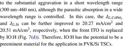
Fig.7.Optical performances of different front TCOs,showing curves of wavelength dependent(a)n and(b)k of different TCO materials,(c)absorptance of front TCO layers,and(d)absorptance of CsPbI3 layer and Si bulk.
2.5. Device performance


Fig.8.Simulated EQE of subcells and optical losses(parasitic absorption,reflectance,and transmittance)of optimized CsPbI3/TOPCon TSC,expressed

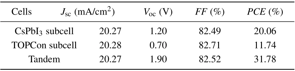
Table 2. Simulated photovoltaic parameters of CsPbI3/TOPCon TSC.
3. Conclusions
The optical performance of CsPbI3/TOPCon twoterminal TSCs is simulated by the combination of ray-tracing and TMM. Compared with planar front surface, bifacial texture can significantly enhance the absorption of both CsPbI3layer and Si bulk due to the reduced front reflection triggered off by the front texture. Meanwhile, the b-IP textured TSC has a more superior photogenerated current density than b-UP

Acknowledgements
The authors would like to thank Prof. Xiaolong Du and Dr. Yaoping Liu for the inspiring discussion.
Project supported by the National Natural Science Foundation of China(Grant Nos.61904201 and 11875088)and the Guangdong Basic and Applied Basic Research Foundation,China(Grant No.2019B1515120057).
猜你喜欢
校园英语·中旬(2022年3期)2022-04-23
湘潮(2021年12期)2021-04-15
Plasma Science and Technology(2021年2期)2021-02-27
方圆(2020年13期)2020-08-09
今古传奇·故事版(2019年2期)2019-02-14
方圆(2017年17期)2017-10-11
天池小小说(2009年9期)2009-09-22
故事林(2008年16期)2008-05-14
现代妇女(1999年11期)1999-06-13
- Chinese Physics B的其它文章
- Direct measurement of two-qubit phononic entangled states via optomechanical interactions
- Inertial focusing and rotating characteristics of elliptical and rectangular particle pairs in channel flow
- Achieving ultracold Bose–Fermi mixture of 87Rb and 40K with dual dark magnetic-optical-trap
- New experimental measurement of natSe(n,γ)cross section between 1 eV to 1 keV at the CSNS Back-n facility
- Oscillation properties of matter–wave bright solitons in harmonic potentials
- Synchronously scrambled diffuse image encryption method based on a new cosine chaotic map