
Phosphorus diffusion and activation in fluorine co-implanted germanium after excimer laser annealing
2022-09-24 08:04ChenWang王尘WeiHangFan范伟航YiHongXu许怡红YuChaoZhang张宇超HuiChenFan范慧晨ChengLi李成andSongYanCheng陈松岩
Chinese Physics B 2022年9期
关键词:李成
Chen Wang(王尘) Wei-Hang Fan(范伟航) Yi-Hong Xu(许怡红) Yu-Chao Zhang(张宇超)Hui-Chen Fan(范慧晨) Cheng Li(李成) and Song-Yan Cheng(陈松岩)
1Fujian Provincial Key Laboratory of Optoelectronic Technology and Devices,School of Opto-electronic and Communiction Engineering,Xiamen University of Technology,Xiamen 361024,China
2Department of Physics,Semiconductor Photonics Research Center,Xiamen University,Xiamen 361005,China
Keywords: phosphorus diffusion, activation concentration, co-implanted fluorine, germanium, excimer laser annealing
1. Introduction
Germanium (Ge) is regarded as a promising high mobility channel material that can replace silicon for postsilicon complementary metal-oxide-semiconductor (CMOS)processing. It owns high electron and hole mobility, low process temperature as well as high absorption coefficient in optical communication band.[1,2]These advantages make it widely used in many devices, such as photo-detectors,[3]sensors,[4]and metal-oxide-semiconductor field-effect transistors (MOSFETs).[5]N-type doping of Ge with high active dopant concentration is an important issue for both CMOS field-effect transistors and optoelectronic applications. As an example, highly doped n-type layer in PIN photodetector structure or in source/drain region in MOSFET structure has played an important role in the performance of devices. Besides,the n-type doping level as high as 1×1020cm-3activation concentration with low diffusion is usually necessary for a downscaling beyond 15 nm. However, it is hard to fulfill the high level n-type doping in Ge because of low solid solubility and large diffusion coefficient of V-group impurity,[6]which will restrict its applications to some extent. In order to obtain heavy n-type doping in Ge, the combination of ion implantation and post-annealing process is frequently utilized.[7]After ion implantation, the severe crystal damage will be formed and induce a number of point defects consisting of Ge vacancies and self-interstitial Ge atoms. As is well known,the diffusion of most n-type dopants in Ge is based on vacancy-assisted mechanisms in the post-annealing process.[8]Recently, the laser annealing technique has been considered as a very promising method to achieve high carrier concentration doping in Ge beyond the solid solubility limit due to its high temperature (beyond the melting point) and metastable state annealing process.[9]Up to now,many reports[10-14]have been devoted to the obtainment of high n-type doping concentration in Ge by using laser annealing,which is verified to be an efficient means for restoration of ion implantation damages. However,it encounters a contradiction between high activation concentrations needed by high laser annealing energy density and low energy density required by shallow junction(narrow dopant profile).
The defect engineering was employed to control the impurity diffusion by modulating the number of trapped vacancies through using co-implantation technique.Many elements,such as carbon(C),nitrogen(N),and fluorine(F),have proved to be alternative co-doping ions to suppress dopant diffusion in the post-annealing process.[15-17]Among those elements,theoretical and experimental studies[13,18-22]show that F owns a large electro-negativity and has been confirmed to be one of the best options because of its higher bonding energy with vacancy to form FnVmclusters than n-type dopants.
In this work, the diffusion and activation of phosphorus in co-implanted P+F Ge after being annealed under different conditions are investigated in detail. Two annealing methods,namely excimer laser annealing(ELA)and rapid thermal annealing(RTA),are used to explore the effects of F on the diffusion and activation of phosphorus in Ge. The evidence and mechanism of F suppressing P diffusion in Ge are suggested by annealing P-only implanted and P+F co-implanted Ge by using ELA and RTA.
2. Experiments
A thickness of~450-µm p-Ge with (100) orientation and a resistivity of 0.05 Ω·cm-1 Ω·cm was employed as a substrate. The Ge substrates were cleaned ultrasonically by being immersed in acetone, ethanol, and de-ionized water, each for 10 min. And the sequence was repeated three times. Next,they were dipped into hydrofluoric acid solution (HF:H2O=1:50) for 30 s to etch off the entire native oxide layer. Finally, all samples were rinsed with de-ionized water for 10 min and dried with high purity nitrogen. Before co-implantation,a 13-nm-thick silicon dioxide film was grown on the surface of Ge substrate by radio frequency magnetron sputtering. And then,two kinds of the samples were prepared.Among the samples of the first kind, some substrates could be implanted only by phosphorous ion with injection energy of 30 keV and a dose of 5×1015cm-2. Phosphorus (P) is a preferable implanted dopant into Ge because other n-type doped impurities,such as antimony and arsenic,will generate more ion implantation damages. Moreover, they own higher impurity diffusion coefficient with abundant vacancies. And among the samples of the other kind,some substrates could be co-implanted by phosphorus(P)and fluorine(F).The implantation condition of phosphorous ion is the same as that in the first kind of sample. After P implantation, fluorinions were implanted into Ge substrate with injection energy of 20 keV and a dose of 5×1014cm-2again. Prior to carrying out any post-annealing process, the SiO2film deposited on substrate surface was etched off by using HF:H2O=1:20 solution at room temperature. And then, all of the implanted samples were ultrasonically cleaned in deionized water for 15 min so as to eliminate the intrinsic oxide layer on Ge surface, which is speculated to be the source of oxygen contaminant during the annealing of Ge.[23]
After that, the samples with implanted P-only and P+F were annealed by two kinds of annealing methods, namely ELA and RTA,respectively. The annealing conditions of ELA on samples were 100 mJ/cm2and 175 mJ/cm2with one pulse,respectively. The ELA process was performed by a 248-nm KrF excimer laser(Coherent Inc. from USA)with 25-ns pulse duration in nitrogen environment. The light spot size during laser annealing was 5 mm×4 mm. In thexdirection and theydirection, the continuous laser scanning was carried out to include the entire sample. The RTA process condition fixed at 650°C for 15 s under nitrogen atmosphere was chosen because it might be the suitable condition to activate implanted ion and repair the implantation damages.[24]
The profiles of P and F chemical concentrations with the varied depths were acquired by using dynamic secondary-ionmass spectrometry (SIMS) PHI ADEPT 1010 instrument. A Cs+primary ion beam with an accelerating voltage of 2 kV,a current of 30 nA and an incident angle of 60°was employed.The carrier concentration depth profiles were obtained by the SSM2000 nano-spreading resistance probe (SRP) measurement system. Samples were beveled using a 0.1-micron diamond paste to have a bevel angle of 0.5°and a depth resolution of about 30 nm. For measurement we used tungsten-osmium probes with a load of 5 grams,probe spacing 80µm and 5-mV small bias applied between two probes. The cross-sectional high-resolution transmission electron microscopy (HRTEM)was used on the co-implanted samples to demonstrate the crystal structure of Ge before and after being annealed by 175-mJ/cm2laser. The Raman spectra of the co-implanted samples were measured to display the restoration of the crystalline structure before and after being annealed under different conditions.
3. Results and discussion
The profiles of phosphorus and fluorine in the samples implanted with P-only and P+F before and after annealing are characterized by SIMS measurement as shown in Fig. 1.Through integrating SIMS profiles,the real dose of phosphorus and fluorine in implanted sample without annealing are 4.72×1015cm-2and 3.1×1014cm-2after the SiO2has been wiped off, respectively. Moreover, the dose loses and the depths for the samples with implanted P-only and P+F after being annealed under various conditions are calculated and displayed in Table 1. As can be seen in Fig. 1(a), a slight diffusion of phosphorus happens and the dopant dose loss is 11.7% in sample A after being annealed by a 100-mJ/cm2laser. By contrast,there is little diffusion or the rearrangement of phosphorus, and only 4% dopant dose is lost in the sample B. Besides, the diffusion redistribution of fluorine seems to happen in 55-nm depth range with 7% dopant dose lost.Figure 1(b) shows the dopant profiles of samples C and D with ELA at 175 mJ/cm2. In the phosphorus there happens impurity diffusion with a length~141 nm at the concentration of 1×1018cm-3and the dopant dose loss reaches up to 36.2% in sample C with P-only implantation. The sample D with P+F co-implantation, by contrast, exhibits a halved phosphorus dopant dose loss of about 16.9% and a depth of~129 nm. Moreover, the diffusion redistribution of fluorine is enhanced to some extent,and the dopant dose loss increases to 12.3%. Based on the above analysis,the reduced phosphorus dopant depth and dose loss by the co-implanted fluorine element may be attributed to the reduction of the number of vacancies,[13,18]which is consistent with the phenomenon in other reports.[19,20]In order to further clarify the effect of the co-implanted fluorine,the RTA process(at 650°C for 15 s)is also conducted in sample E and sample G,and the profiles of P and F are displayed in Fig.1(c).As we can see from the figure,the phosphorus shows a box-shaped distribution in each of the two samples. An obvious diffusion of the phosphorus with a depth~288 nm occurs, and the dopant doseloss rises up to 73.3%in sample E with P-only implantation. However,sample G with P+F co-implantation,by contrast,shows a reduced phosphorus dopant dose loss of about 56.6% and a depth of~236 nm. It is worth noting that the diffusion of fluorine element is controlled by external diffusion and fluorine dose loss increases up to 95.7%. This interesting phenomenon may be due to the pre-etching of surface SiO2prior to annealing and is consistent with other reported result.[20]In summary,the diffusion of phosphorus can be suppressed to some extent because of the fluorine co-implantation in Ge, whether using ELA process or RTA process.

Fig.1. SIMS profiles of P and F accessed from the samples implanted with P-only and P+F before and after one pulse laser annealing at(a)100 mJ/cm2,(b)175 mJ/cm2,and(c)annealing at 650 °C for 15 s.
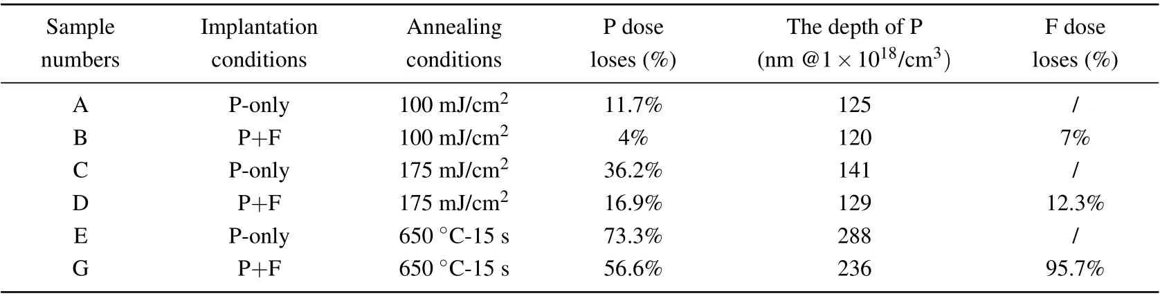
Table 1. Dose looses,depths for samples implanted by P-only and P+F under various annealing conditions.
For further exploring the role of fluorine during the phosphorus diffusion after ELA process, the non-equilibrium mechanism in ultra-fast melting and recrystallization process of co-implanted P+F Ge need further investigating. When the excimer laser with an enough laser energy density irradiates the surface of Ge, a melted zone will be well defined,resulting in an abrupt transition between the liquid and solid phase Ge. In our previous studies,[24,25]an analytical model was proposed to predict the impurity diffusion profiles under various laser annealing energy densities and the impurity diffusion occurring and being controlled in the melting region mostly. Based on this model,[24]the SIMS profiles of P in samples C and D are simulated and fitted after ELA without taking into account the surface recombination or segregation of phosphorus. The well fitting curves (represented by continuous lines)are shown in Fig.2 through optimizing the parameters. Hence, the diffusion coefficient of phosphorus in the melting region of sample C and sample D are obtained to be about 3.94×10⁻⁴cm2/s and 3.45×10⁻⁴cm2/s, respectively. The reduced diffusion coefficient can be explained below. After being implanted by P ions, the amorphous Ge is formed and the F ions implanted in Ge are more likely to form F interstitials.[13,18,20]And then, the F interstitials will combine with vacancies to form FnVmclusters quickly during the initial phases of laser annealing[20]because FnVmclusters has a higher bonding energy than FGei(F bonding with Ge interstitials).[13,18]Moreover,in the amorphous Ge region,there exist a large number of vacancies and the diffusion of P is vacancy-assisted diffusion during the ELA.[25]However,these FnVmclusters are stable and can possibly stabilize the excess vacancies. Hence,the fewer vacancies can take part in the diffusion of P in the melting region,leading to the shorter P diffusion depth than those without F ions implantation. Besides,in the laser annealing process, the amorphous Ge is gradually crystallized because the interaction between Ge interstitials and FnVmclusters results in the elimination of vacancies and the release of mobile F interstitials. The SiO2capping layer is removed so that it cannot inject interstitials into Ge to help annihilate the vacancies. Moreover, the F atoms will escape from Ge into the outside by high-mobile F interstitials quickly,which is the possible reason for the F dose loss as high as 95.6%after RTA process.
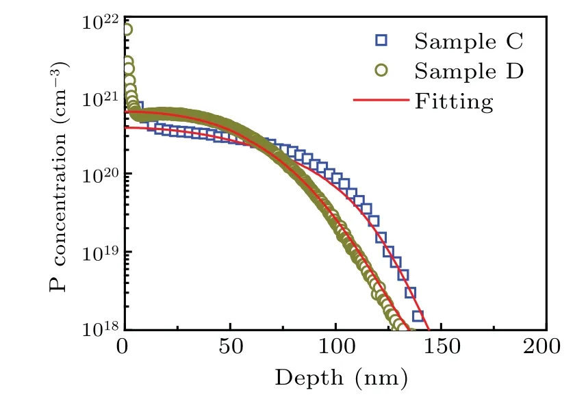
Fig. 2. Simulated (red solid line) and measured (empty square and empty circle)P profiles of the samples C and D with ELA at 175 mJ/cm2.
The activation concentrations of phosphorus at a fixed depth of about 30 nm in germanium under different annealing conditions are characterized by the SRP measurement as shown in Fig. 3. For the sample A and sample B with ELA at 100 mJ/cm2, their carrier concentrations are as low as 7.9×1018cm-3and 9.2×1018cm-3, respectively, which can be attributed to the deficient laser energy values needed to annihilate the implantation damages and activate dopants,which will be confirmed by Raman spectrum next. As for the samples C and D each irradiated by an increased laser fluence of 175 mJ/cm2, their activation concentrations of phosphorus are 2.7×1020cm-3and 4.4×1020cm-3, respectively, which is beyond the phosphorus solid solubility limit in Ge in the ELA process.[10]Moreover, the samples E and G with RTA at 650°C for 15 s acchieve their activation concentrations of 4.2×1019cm-3and 5.3×1019cm-3,respectively. The higher carrier concentration in sample G with co-implantation is due to the narrower P profile than the sample E.Furthermore,comparing the ELA method with the RTA method,the ELA combined with co-implanted F ion is a more efficient technique to achieve high-activation-concentration doped n-Ge with narrow dopant profile than those obtained by RTA process.
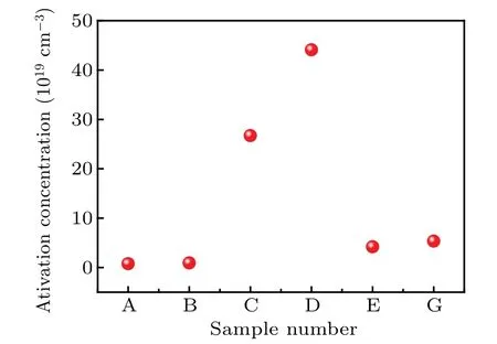
Fig.3. Activation concentrations at 30-nm depth,obtained by SRP,for samples A,B,C,D,E,and G respectively.
The Raman spectra for the as-implanted P+F and P-only samples before and after being annealed under different conditions are characterized and shown in Fig. 4. For the asimplanted P+F and P-only samples without being annealed,the broad peak of amorphous Ge (a-Ge) phase centered at about 270 cm-1indicates that the surfaces of Ge substrates are severely damaged,resulting in the formation of amorphous Ge layer after implantation process. After ELA at 100 mJ/cm2,both of them show that the Ge-Ge optical phonon mode representing crystallized Ge(c-Ge)near 300 cm-1appears while the peak of a-Ge still exists in the spectrum. It can be due to the fact that the deficient laser annealing energy gives rise to the partial restoration of implantation-damaged lattices. When the as-implanted P+F and P-only samples are annealed at 175 mJ/cm2, the peak of a-Ge disappears and only crystal Ge peaks are observed with a low full-width at half-maximum(FWHM)value of about 7.2 cm-1and 7.4 cm-1,respectively.Hence,it can be suggested that the ELA is an effective annealing method to repair the lattice damages induced by mixed ion implantation. It will also be confirmed by the HRTEM image in Fig. 5(b) in the following. Moreover, the Raman spectra of the samples E and G with RTA process also show only c-Ge peaks with an FWHM of about 7.67 cm-1and 7.6 cm-1,respectively.

Fig.4. Raman spectra of P+F co-implanted and P-only implanted samples before and after being annealed under different conditions.
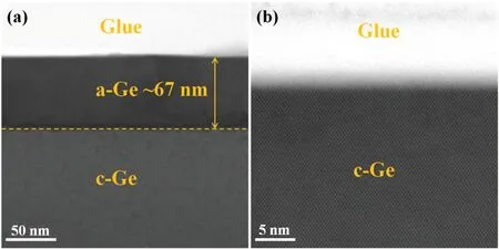
Fig. 5. Cross-sectional HRTEM images of co-implanted P+F samples (a)before and after(b)being annealed by laser at 175 mJ/cm2.
The structures of co-implanted P+F samples before and after ELA at 175 mJ/cm2are explored by cross-sectional HRTEM as shown in Figs.5(a)and 5(b). It can be seen from Fig. 5(a) that a 67-nm-thick amorphous Ge layer is formed with a clear amorphous/crystal interface due to severe damage induced by high energy and dose mixed ion implantation.After ELA at 175 mJ/cm2,almost no extending defect can be detected as shown in Fig.5(b),which indicates that the amorphous Ge layer is transformed into crystal Ge completely. It is consistent with the result of Raman analysis in Fig.4.
4. Conclusions
Both excimer laser annealing process and rapid thermal annealing process are utilized to investigate the diffusion and activation of phosphorus in phosphorus and fluorine coimplanted Ge. No matter what annealing methods are used,the co-implanted fluorine can reduce phosphorus diffusion and enhance phosphorus activation during the annealing. It is attributed to the formation of high bonding energy FnVmclusters which can eliminate some excess vacancies resulting in the reduced vacancy-assisted diffusion of phosphorus. The laser density of 100 mJ/cm2is not high enough to crystallize implantation induced amorphous Ge layer while a maximum activation concentration of about 4.4×1020cm-3with a reduced diffusion length and dopant loss is achieved at 175 mJ/cm2in P+F co-implanted Ge. Moreover, the ELA process is more efficient to reduce diffusion length and promote activation concentration than the RTA process. In conclusion, the combination of excimer laser annealing and co-implantation techniques will be a very promising method to fulfill highactivation and shallow-diffusion n-type doping in Ge.
Acknowledgements
Project supported by the National Natural Science Foundation of China(Grant No.61904155),the Science and technology Project of Fujian Provincial Department of Education,China (Grant No. JAT200484), the Natural Science Foundation of Fujian Province, China (Grant No. 2018J05115), and the Scientific Research Projects of Xiamen University of Technology,China(Grant No.YKJCX2020078).
猜你喜欢
中等数学(2022年9期)2022-11-17
东坡赤壁诗词(2022年4期)2022-10-30
今日农业(2021年17期)2021-11-26
西部论丛(2018年11期)2018-10-19
中国(韩文)(2018年6期)2018-06-25
中国(韩文)(2018年1期)2018-01-17
棋艺(2016年4期)2016-09-20
微型小说选刊(2015年22期)2015-11-17
现代营销·经营版(2011年8期)2011-05-14
- Chinese Physics B的其它文章
- Characterizing entanglement in non-Hermitian chaotic systems via out-of-time ordered correlators
- Steering quantum nonlocalities of quantum dot system suffering from decoherence
- Probabilistic quantum teleportation of shared quantum secret
- Spin–orbit coupling adjusting topological superfluid of mass-imbalanced Fermi gas
- Improvement of a continuous-variable measurement-device-independent quantum key distribution system via quantum scissors
- An overview of quantum error mitigation formulas