
Lattice damage in InGaN induced by swift heavy ion irradiation
2022-10-26 09:51NingLiu刘宁LiMinZhang张利民XueTingLiu刘雪婷ShuoZhang张硕TieShanWang王铁山andHongXiaGuo郭红霞
Chinese Physics B 2022年10期
Ning Liu(刘宁) Li-Min Zhang(张利民) Xue-Ting Liu(刘雪婷) Shuo Zhang(张硕)Tie-Shan Wang(王铁山) and Hong-Xia Guo(郭红霞)
1State Key Laboratory of Laser Interaction with Matter,Northwest Institute of Nuclear Technology,Xi’an 710024,China
2School of Nuclear Science and Technology,Lanzhou University,Lanzhou 730000,China
Keywords: InGaN,swift heavy ions,irradiation effects
1. Introduction
Indium gallium nitride(InGaN)is an important group III nitride semiconductor material. The bandgap of InxGa1-xN can be tuned from 0.7 eV to 3.4 eV with decreasing In contentxfrom 1 to 0,[1,2]which covers nearly the whole solar spectrum. Hence, InGaN has great potential for the development of multi-junction solar cells,light-emitting diodes(LEDs)and laser diodes (LDs).[3]One of the challenges for the application of InGaN materials is how to achieve p-type doping, in particular for In-rich InxGa1-xN(x >0.5).[1]The ion implantation technique is widely used for ion doping in semiconducting materials.[4,5]As implantation-induced radiation damage is detrimental to effective doping,knowledge of the radiation effects in implanted materials is essential for the application of ion implantation. Over the past decade,extensive research effort has been devoted to radiation studies of InGaN.[6–12]It has been found that the resistance of InGaN to irradiationinduced amorphization dramatically decreases with increasing In concentration in InGaN. While GaN is fully amorphized by room-temperature irradiation of 1 MeV Au ions to a dose of~90 dpa (displacements per atom),[13]the amorphization dose for In0.2Ga0.8N under a similar irradiation condition is only~1.4 dpa.[8]The lattice structure of InxGa1-xN(x ≥0.7)irradiated with 5 MeV Xe ions at room temperature was observed to break down at doses of no more than 0.1 dpa.[9]The decreasing radiation resistance of the high In-content In-GaN is primarily attributed to a smaller cohesive energy of the In–N bond,which results in a reduced dynamic annealing efficiency.[9]However, to date, little is known about the response of InGaN to irradiation with swift heavy ions (SHIs)with ion energies larger than several tens of MeV. Unlike the case of low-energy ion irradiation,huge electronic energy deposition is produced in materials by SHI irradiation.Ion tracks with a modified material structure along the ion incidence direction will be created when the electronic stopping power(Se)of incident ions exceeds a certain threshold;[14]otherwise annealing of the pre-existing lattice defects probably occurs.SHIs with large projected ion ranges can be used for deep ion implantation of materials. In addition, the application of InGaN-based electronics in outer space will suffer from SHI irradiation. Hence it is important to understand the radiation effects of SHIs in InGaN. This work focuses on the dependence on In content of radiation hardness of InGaN to SHI irradiation. Both In0.32Ga0.68N and In0.9Ga0.1N films are irradiated with 2.25 GeV Xe ions and then characterized by high-resolution x-ray diffraction(HRXRD),Raman scattering,Rutherford backscattering spectrometry in channeling geometry (RBS/C) and transmission electron microscopy (TEM).The reported results will improve the current understanding of SHI irradiation-induced damage effects in InGaN,and may have important implications for the ion implantation and space electronics of InGaN materials.
2. Experiments
The wurtzite InxGa1-xN films used in this work were grown by metal–organic chemical vapor deposition(MOCVD)onc-plane sapphire(Al2O3)substrates with 2 μm thick GaN interlayers. Based on the analysis of Rutherford backscattering spectrometry (RBS), the In contentxin the two different InxGa1-xN samples was determined to be 0.32 and 0.9±0.01, respectively; the film thicknesses of the In0.32Ga0.68N and In0.9Ga0.1N were~290 nm and 350 nm.The samples were cut into 4 mm×4 mm squares for ion irradiation. SHI irradiation experiments were performed at the Heavy Ion Research Facility in Lanzhou in the Institute of Modern Physics, Chinese Academy of Sciences. The 2.52 GeV129Xe27+ions were provided by the sector-focused cyclotron and sector-separated cyclotron. In order to count and decelerate the Xe ions,high-purity Al foils were placed in front of the samples with the foil surface normal to the incident ion beam. After penetrating the foils,the incident Xe ions are slowed down to an energy of 2.25 GeV according to the SRIM simulation,[15]and they are expected to attain charge-state equilibrium. The mean equilibrium charge state of 2.25 GeV Xe ions in solids is calculated by the CasP code to be 48+.[16]The samples were then irradiated at room temperature and normal incidence to ion fluences of 3×10¹¹ions·cm-2and 7×10¹¹ions·cm-2with a beam flux of 3×10⁸ions·cm-2·s-1.The In0.32Ga0.68N and In0.9Ga0.1N samples were irradiated simultaneously by placing them side by side under a uniform beam spot. The incident Xe ions penetrate the InGaN films and underlying GaN interlayers completely and terminate in the Al2O3substrates. For a comparison study,the In0.9Ga0.1N sample was also irradiated at room temperature with 5 MeV129Xe20+ions at the 320 kV platform for multidisciplinary research at the Institute of Modern Physics, Chinese Academic of Sciences. The irradiation was conducted at normal incidence to a fluence of 3×10¹¹ions·cm-2with a beam flux of 1×10¹¹ions·cm-2·s-1. After irradiation, the samples were characterized by HRXRD using a Bruker D8 diffractometer.ω–2θscans of the(0002)plane of the samples were performed in triple-axis mode with a CuKαsource. The angular resolution of the spectra was 0.005°. The Raman scattering measurements were carried out using a LabRAM HR 800UV spectrometer(Horiba Jobin-Yvon). In order to reduce the Raman signal from the GaN sublayers, the 325 nm line of a Cd–He laser was used as the excitation source. The laser beam was focused onto a spot with a diameter of~3 μm at the sample surface. The Raman spectral resolution was better than 1 cm-1. The RBS/C measurements were performed with a 2 MeV He+ion beam incident along〈0001〉direction of the samples and recorded by a detector at a backscattering angle of 150°or 165°. The backscattering yields have an uncertainty of~7% due to the inaccuracy of current integration.Cross-sectional TEM foils with a thickness of~50 nm were prepared using a focused ion beam system after application of a protective Pt/Au layer on the sample surface. TEM was performed on the samples using FEI TF30 at an accelerating voltage of 300 kV.
3. Results
3.1. HRXRD results
Figure 1 illustrates the HRXRD spectra of the In0.32Ga0.68N and In0.9Ga0.1N (0002) peaks before and after 2.25 GeV Xe ion irradiation to a fluence of 7×10¹¹ions·cm-2.It is seen that the intensities of the InGaN peaks are weak,because the InGaN films are thin and the sample sizes are very small. The full width at half maximum (FWHM) values of the virgin In0.32Ga0.68N and In0.9Ga0.1N are roughly estimated to be 0.14°and 0.06°, respectively. This suggests that the In0.9Ga0.1N film has a better crystal quality than In0.32Ga0.68N. The analysis of the virgin (0002) peaks leads to lattice parameters ofc=0.5386 nm for In0.32Ga0.68N andc=0.5704 nm for In0.9Ga0.1N, respectively. Using Vegard’s law,[17]thec0values of perfect In0.32Ga0.68N and In0.9Ga0.1N are estimated to be 0.5351 nm and 0.5651 nm, with the assumptions ofc0=0.5186 nm for GaN andc0=0.5703 nm for InN. The virgin In0.32Ga0.68N and In0.9Ga0.1N exhibit slight lattice strains [(c-c0)/c0×100%] of~0.6% and 0.9%, which originate from the differences in lattice constants and thermal expansion coefficients between the InGaN and GaN substrates.[1]After Xe ion irradiation,no significant changes in FWHM of the diffraction peaks are induced for either In0.32Ga0.68N or In0.9Ga0.1N. The In0.32Ga0.68N peak in Fig.1(a)exhibits a slight shift of 0.01°towards higher angles with respect to the unirradiated peak.

Fig.1. HRXRD spectra for(a)In0.32Ga0.68N and(b)In0.9Ga0.1N films before and after 2.25 GeV Xe ion irradiation at room temperature to a fluence of 7×10¹¹ ions·cm-2.
Normally, ion irradiation causes lattice expansion in nitride materials, which results in a shift of the diffraction peaks towards lower angles.[18]The abnormal shift of the In0.32Ga0.68N peak may be attributed to a slight compositional difference in those samples. The InGaN samples used in this work are cut from an InGaN wafer grown by MOCVD with a diameter of 2 inches. The In content and film thickness are different in different regions of the wafer. However,the differences are slight and cannot be resolved by RBS and Raman spectroscopy, as shown below. In contrast to In0.32Ga0.68N, the In0.9Ga0.1N peak obviously shifts towards smaller angles. The shift indicates an irradiation-induced lattice expansion in In0.9Ga0.1N, which is ascribed to the accumulation of various point defects,which is common in nitride materials.[10,14]The corresponding lattice strain along thecaxis is increased to 1.1%. The XRD results suggest that, as in the case of low-energy heavy-ion irradiation,[9]the In-rich In0.9Ga0.1N is more sensitive to SHI irradiation than the Garich In0.32Ga0.68N.
3.2. Raman results

Fig. 2. Raman spectra for (a) In0.32Ga0.68N and (b) In0.9Ga0.1N films before and after 2.25 GeV Xe ion irradiation at room temperature to a fluence of 7×10¹¹ ions·cm-2. The inset shows the magnified E2(high)peak from In0.9Ga0.1N.
Figure 2 shows the Raman spectra for the In0.32Ga0.68N and In0.9Ga0.1N films before and after 2.25 GeV Xe ion irradiation to a fluence of 7×10¹¹ions·cm-2. In addition to the E2(high)and A1(longitudinal optical,LO)peaks from the InGaN films, there are two fluorescence-induced background peaks at 323 cm-1and 573 cm-1. For In0.32Ga0.68N, there is a shoulder on the low-frequency side of the A1(LO) peak,which is assigned as a disorder-activated E1(LO) mode due to the poor crystal quality of In0.32Ga0.68N.[19]The intensity of the A1(LO) peak from the In0.9Ga0.1N film is very weak,which is attributed to the increasing electron carrier concentration in In0.9Ga0.1N that damps the LO phonons via phonon–plasmon coupling.[20,21]After Xe ion irradiation, no changes are revealed in the Raman spectrum of In0.32Ga0.68N whereas the E2(high) peak of In0.9Ga0.1N shifts from 497 cm-1to 501 cm-1, as shown in the inset of Fig. 2(b). The blue shift of the E2(high) peak suggests the existence of a compressive stress in the irradiated In0.9Ga0.1N[22]associated with the irradiation-induced lattice expansion. This is in good agreement with the XRD observation in Fig.1.
3.3. RBS/C results
Figure 3 displays the RBS random and〈0001〉-aligned channeling spectra for the In0.32Ga0.68N and In0.9Ga0.1N films on GaN before and after 2.25 GeV Xe ion irradiation to a fluence of 7×10¹¹ions·cm-2. The depth scales of the In and Ga sublattices are obtained using the He stopping power from the SRIM database. The simulation results of random spectra using the SIMNRA 7.0 code[23]are also included in the figures,from which the film composition and thickness are estimated.For the virgin In0.9Ga0.1N,the minimum backscattering yield(χmin) as determined by the yield ratio of the channeling to a random spectrum in the near-surface region is 4.7%, typical for a perfect crystal. By contrast, theχminfor the virgin In0.32Ga0.68N is as high as 47%,which is attributed to the large lattice mismatch between GaN and InN.[1]As shown in Fig.3,Xe ion irradiation leads to little damage in In0.32Ga0.68N, as suggested by the RBS/C yields before and after irradiation.However, the In0.9Ga0.1N is damaged under the identical irradiation condition,which is consistent with the HRXRD and Raman scattering results. The relative In disorder in the irradiated In0.9Ga0.1N,Dr,can be calculated from

whereYvcandYvrare the integrated yields of the channeling and random spectra from the virgin film andYicis the integrated yield of the irradiated channeling spectrum. The backscattering yields are integrated in a small depth region from 50 nm to 75 nm just below the sample surface, where the influence of angular dispersion of the incident He ions on the RBS/C yields can be neglected. TheDrvalue of the Xeirradiated In0.9Ga0.1N film is calculated to be 5%.

Fig. 3. RBS/C spectra together with the random spectra for (a)In0.32Ga0.68N and(b)In0.9Ga0.1N films grown on GaN before and after 2.25 GeV Xe ion irradiation to a fluence of 7×10¹¹ ions·cm-2.The red curves are simulation results of the random spectra using the SIMNRA code.
3.4. TEM results
In order to investigate whether 2.25 GeV Xe ion irradiation leads to the formation of ion tracks in In0.9Ga0.1N, the Xe-irradiated In0.9Ga0.1N sample was characterized by crosssectional TEM. The sample irradiated with an ion fluence of 3×10¹¹ions·cm-2was used for the characterization,because overlapping of ion tracks probably occurs in the TEM image at a larger fluence.[24]The TEM image of the Xe-irradiated sample is shown in Fig.4(a),together with the corresponding selected area electron diffraction pattern. Dislocation loops(black spots) as well as dislocation lines that penetrate the In0.9Ga0.1N film along the film growth direction are observed.These dislocations also exist in the pristine In0.9Ga0.1N(data not shown),implying that they are formed during the epitaxial growth of the In0.9Ga0.1N film, which is common for nitride films.[25,26]Figure 4(b) shows the high-resolution TEM image of the Xe-irradiated In0.9Ga0.1N together with the corresponding fast-Fourier transform pattern. The In0.9Ga0.1N exhibits an intact lattice structure after irradiation. Assuming that highly disordered or amorphous ion tracks are formed in In0.9Ga0.1N, the track diameter should be~3 nm (estimated from the RBS/C spectra). The detailed calculation method can be found in Ref. [14]. However, no such ion tracks are revealed in the TEM image. This suggests that point defects and/or small defect clusters are probably the dominant defect types in the Xe-irradiated In0.9Ga0.1N,and these cannot be resolved by conventional TEM.Instead,XRD,Raman scattering and RBS/C are very sensitive to these defects.

Fig.4. (a)Cross-sectional TEM image and corresponding selected area electron diffraction pattern and(b)high-resolution TEM image and corresponding fast Fourier transform pattern of In0.9Ga0.1N irradiated with 2.25 GeV Xe ions to a fluence of 3×10¹¹ ions·cm-2.
4. Discussion
In the present study,In0.9Ga0.1N is found to be more sensitive to 2.25 GeV Xe ion irradiation than In0.32Ga0.68N.This agrees well with our previous irradiation study of InxGa1-xN(x=0.32–1.0) using 5 MeV Xe ions, which shows that the radiation resistance of InGaN decreases with increasing In concentration.[9]The decreasing radiation resistance of Inrich InGaN is mainly attributed to the smaller cohesion energy of the In–N bond (7.970 versus 9.058 eV/atom for the Ga–N bond). As a consequence, the broken In–N bonds are more difficult to restore than Ga–N bonds,which reduces the dynamic annealing efficiency in In-rich InGaN. In addition,the formation enthalpy of InGaN decreases with increasing In concentration, which leads to a decrease in the intrinsic stability of In-rich InGaN.[9]However,unlike the case of 5 MeV Xe ion irradiation, 2.25 GeV Xe ion irradiation creates lattice damage in In0.9Ga0.1N, primarily via intense electronic excitation rather than ballistic collision. For comparison, the In0.9Ga0.1N sample irradiated with 5 MeV Xe ions at room temperature to a fluence of 3×10¹¹ions·cm-2was characterized by RBS/C, and the results are shown in Fig. 5. According to the SRIM calculation, the projected range of 5 MeV Xe ions in the InGaN/GaN samples is~1.1 μm, which is about four times greater than the thickness of the In0.9Ga0.1N film. Hence, the incident Xe ions penetrate the In0.9Ga0.1N film and create a nearly homogeneous damage distribution in the film. It is seen from Fig.5 that 5 MeV Xe ion irradiation leads to little increase in RBS/C yields. TheDrvalue estimated from the near-surface region of the film is only 1.7%,which is lower than the value of 5% induced by 2.25 GeV Xe ion irradiation at 7×10¹¹ions·cm-2. The corresponding SRIM-calculated displacement damage dose at the nearsurface region is 6×10⁻⁴dpa for 5 MeV Xe irradiation of 3×10¹¹ions·cm-2,but only 1.3×10⁻⁵dpa for 2.25 GeV Xe irradiation of 7×10¹¹ions·cm-2. This means that 2.25 GeV Xe ion irradiation leads to a higher lattice disorder with a much lower displacement damage dose. Obviously, the huge electronic energy deposition accounts for the damage production in In0.9Ga0.1N irradiated with 2.25 GeV Xe ions. According to the thermal spike model,[27–31]target electrons are excited as a result of extremely high electronic energy deposition under SHI irradiation. The excited electrons transfer their energy to lattice atoms via electron–phonon coupling in a few picoseconds. This strong coupling effect between electronic and atomic subsystems can result in the formation of atomiclevel defects.[32]
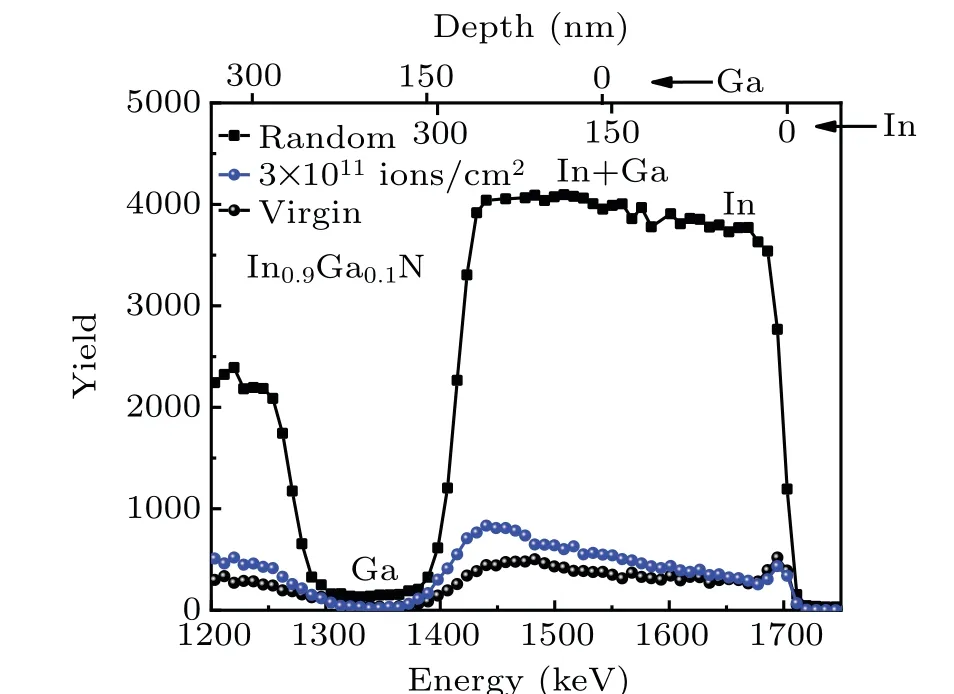
Fig.5. RBS/C spectra together with the random spectra for In0.9Ga0.1N films on GaN/Al2O3 before and after 5 MeV Xe ion irradiation at room temperature to a fluence of 3×10¹¹ ions·cm-2.
Although 2.25 GeV Xe ion irradiation produces lattice damage in In0.9Ga0.1N, no ion tracks are observed to be formed. It was found that theSethreshold for ion track formation in GaN is between 22.8 keV·nm-1and 28.3 keV·nm-1.[33]InGaN and InN were found to be more susceptible to SHI irradiation than GaN.[9,14]For InN, ion tracks of 3.6 nm in diameter are created by 104 MeV Pb ions with aSevalue of 22 keV·nm-1.[30]TheSevalue of 2.25 GeV Xe ions in In0.9Ga0.1N is calculated by SRIM to be 23 keV·nm-1. The absence of ion tracks in Xe-irradiated In0.9Ga0.1N could be attributed to the very high velocity of the Xe ions. For SHIs in solids, the higher the ion velocity, the larger the volume in which the electronic energy is deposited(the so-called velocity effect).[34–36]As a result,ion tracks are more likely to be formed for SHIs with a lower velocity because of the larger electronic energy deposition density. Using the inelastic thermal spike model,[30]theSethresholds for the formation of ion tracks in InN and GaN were predicted to increase with increasing ion velocity from 0.5 MeV·u-1to 4.5 MeV·u-1. Since the velocity of 2.25 Xe ions is as high as 17 MeV·u-1, the electronic energy deposition density of the Xe ions in In0.9Ga0.1N could be too low to induce ion tracks.Point defects and defect clusters are therefore expected to be the dominant defect type in the Xe-irradiated In0.9Ga0.1N.
5. Conclusions
Wurtzite In0.32Ga0.68N and In0.9Ga0.1N films were irradiated with 2.25 GeV Xe ions to 3×10¹¹ions·cm-2and 7×10¹¹ions·cm-2at room temperature. The irradiated films were analyzed by HRXRD, Raman scattering, RBS/C and TEM.The radiation resistance of InxGa1-xN was found to decrease with increasing In contentx. The HRXRD and Raman scattering results show that Xe ion irradiation leads to lattice expansion along with lattice strain in In0.9Ga0.1N.By contrast,there are almost no structural changes in In0.32Ga0.68N under identical radiation conditions. The level of lattice disorder,as determined by RBS/C, increases in In0.9Ga0.1N after irradiation. The intense electronic excitation rather than ballistic collision is confirmed to account for the production of damage.However, no ion tracks were observed in the TEM images of Xe-irradiated In0.9Ga0.1N, which is due to the velocity effect of SHIs in solids.Point defects and/or small defect clusters are probably the main radiation damage in In0.9Ga0.1N,and these cannot be resolved by conventional TEM but are very sensitive to XRD,Raman scattering and RBS/C.
Acknowledgements
The authors thank the staff of the Heavy Ion Research Facility in Lanzhou and the 320 kV platform in the Institute of Modern Physics, Chinese Academy of Sciences for support with the ion irradiation. We are grateful to Professor R.C. Fadanelli at the Federal University of Rio Grande do Sul,Brazil for his kind help with the RBS/C measurements.
Project supported by the National Natural Science Foundation of China(Grant No.11875154)and State Key Laboratory of Intense Pulsed Radiation Simulation and Effect(Grant No.SKLIPR2014).
猜你喜欢
海外文摘·学术(2022年3期)2022-05-07
小学生作文·小学低年级适用(2022年4期)2022-04-27
短篇小说(原创版)(2021年9期)2021-01-03
作文周刊·小学一年级版(2020年40期)2020-10-19
37°女人(2019年9期)2019-12-16
中国工人(2018年7期)2018-07-17
小小说月刊·下半月(2017年7期)2017-07-25
民间故事选刊·下(2017年6期)2017-06-14
试题与研究·中考化学(2016年1期)2016-09-30
中学生数理化·八年级物理人教版(2015年10期)2016-01-04
- Chinese Physics B的其它文章
- Formation of high-density cold molecules via electromagnetic trap
- Dynamics of molecular alignment steered by a few-cycle terahertz laser pulse
- Terahertz spectroscopy and lattice vibrational analysis of pararealgar and orpiment
- Molecule opacity study on low-lying states of CS
- Finite-time Mittag–Leffler synchronization of fractional-order complex-valued memristive neural networks with time delay
- Ultrafast Coulomb explosion imaging of molecules and molecular clusters