
Recombination-induced voltage-dependent photocurrent collection loss in CdTe thin film solar cell
2022-10-26 09:54LingLingWu吴玲玲GuangWeiWang王光伟JuanTian田涓DongMingWang王东明andDeLiangWang王德亮
Chinese Physics B 2022年10期
关键词:王东明
Ling-Ling Wu(吴玲玲), Guang-Wei Wang(王光伟), Juan Tian(田涓),Dong-Ming Wang(王东明), and De-Liang Wang(王德亮)
Hefei National Laboratory for Physical Sciences at Microscale,University of Science and Technology of China,Hefei 230026,China
Keywords: CdTe solar cell, voltage-dependent photocurrent collection efficiency, interface recombination,bulk recombination
1. Introduction
CdTe thin film solar cell has proved to be one of the most competitive thin film photovoltaic devices because of its high conversion efficiency, excellent long-term stability and low cost. The record power conversion efficiency (PCE) of the CdTe solar cell and the module have reached 22.1% and 18.6%, respectively.[1,2]The latest increase in PCE is mainly attributed to redevelopment of device window layer structure,which has dramatically improved short-circuit current(Jsc)of devices.[3,4]The CdS thin film is usually used as the window layer in CdTe solar cell. However, with a bandgap (Eg) of 2.45 eV,CdS exhibits parasitic absorption of short wavelength light (<510 nm).[5,6]This can result in aJscloss of about 5 mA/cm2.[7]Researchers has tried reducing parasitic absorption by incorporating moderate oxygen into CdS and/or thinning this layer.[6,8]Recently,alternatives to CdS have been investigated,such as MgxZn1-xO(MZO)and CdSe.[9–12]
The MZO proved to be a promising material for window layer of CdTe solar cell,because it has a tunableEgin a range of 3.37 eV–7.6 eV by varying the Mg content.[13]A window layer material with highEgcan improve spectral response and increaseJsc. When the MZO film with an appropriate Mg content contacts CdTe film, a slight spike will be formed in the conduction band (CB) at the p–n junction interface. This slight spike can help reduce the interface recombination and improve carrier collection.[14,15]Munshiet al.obtained CdTe solar cell with a maximum conversion efficiency of 18.7%by using Mg0.23Zn0.77O as a window layer.[15]However, highefficiency MZO/CdTe solar cell has not been reproduced by other research groups. One of the causes is the“S-kink”phenomenon, which is attributed to improper conduction band offset (CBO) between the MZO and CdTe interfaces.[16,17]However,even if the“S-kink”is eliminated,MZO/CdTe solar cell still has a low fill factor (FF). Delahoyet al. eliminated“S-kink” by using higher CdTe deposition temperature and a thinner MZO layer. The efficiency of the cells increased from 4.2%to 10.5%.[17]However,theFFincreased to 47.8%only.Bittauet al. also increased the substrate temperature during CdTe deposition. And higherFFwas obtained with an average value about 63%.[18]Since the MZO film was sensitive to the oxygen during the solar cell preparation process,[16,19]several researchers have tried removing oxygen in absorber deposition and/or CdCl2treatment process. Liet al. reported a significant increase inFFfrom 44.8%to 72.9%through an oxygen-free CdCl2treatment.[16]Similar work has been done by Ablekimet al.,butFFwas only raised to 55.4%.[19]
In our previous work,[13]the “S-kink” was eliminated by optimizing MZO preparation and heat treatment process.In this work, a comparative study between MZO/CdTe and CdS/CdTe solar cells with similar efficiency is carried out.The PCE loss induced by voltage-dependent current collection(ηC(V′))is quantified. The time-resolved photoluminescence(TRPL)and the temperature-dependent current densityvoltage(J–V–T)are measured and SCAPS simulation is performed to investigate the causes for lowFFand poor performance of the MZO/CdTe solar cell. And the result shows that more severe carrier recombination in the MZO/CdTe solar cell is responsible for the worse performance than in the CdS/CdTe solar cell.
2. Experiment
As shown in Fig.1,the CdTe solar cells had a structure of glass/SnO2:F(FTO)/window layer/p-CdTe/ZnTe:Cu/Au. The intrinsic SnO2interlayer in CdS/CdTe solar cell acted as a high resistance layer. And both window layers were deposited on glass/FTO (14 Ω/sq, NSG) substrates via radio frequency(RF) magnesium sputtering. The thicknesses of SnO2, CdS,and MZO films were 40, 80, and 60 nm, respectively. The MZO films had an Mg:Zn atomic ratio of 0.1:0.9. The SnO2,CdS and MZO targets of 99.99% purity were used in this work. The deposition atmosphere was a mixture of O2and Ar during sputtering. The volume ratio of O2was 40% for SnO2deposition and a small quantity of O2(1%–6%)was introduced during CdS and MZO sputtering. The as-deposited CdS films were then annealed in CdCl2atmosphere to obtain high-quality crystal. The P-type CdTe absorption layers(~4-μm thick)were deposited by a homemade close-spaced sublimation(CSS)system. The deposition atmosphere was Ar:O2mixture for the CdS/CdTe solar cells. And it was pure Ar for the MZO/CdTe solar cells. Subsequently, both stacks were thermally activated in the presence of CdCl2. Before depositing the back contact films,the activated CdTe surface is chemically etched by nitric-phosphoric solution. Then, a 100-nmthick Cu-doped ZnTe(ZnTe:Cu)buffer layer and an Au electrode were successively evaporated on the etched CdTe surface. Finally,the solar cells were rapidly annealed to activate the ZnTe:Cu. Notably,because MZO film is very sensitive to oxygen,[16,19,20]oxygen was avoided throughout the preparation of MZO/CdTe solar cells except for MZO depositing.
The morphological microstructures of CdTe films were characterized by using a field emission scanning electron microscope (SEM, SU8200, HITACHI). The current density–voltage (J–V) of all solar cells were measured under standard AM1.5 illumination (1 kW·m-2, 25°C) by using a solar simulator(Oriel Sol 3A,USA).Two light filters were used to obtain monochromatic light centered at 532 nm with a full width at half maximum(FWHM)of 10 nm and infrared light with wavelength higher than 850-nm irradiation. For simplicity, these illumination conditions are named 1 sun, 532-nm monochromatic and infrared illumination hereinafter. AndJ–V–Tcharacteristics were performed by using a liquid-N2-cooled cryostat(LT3-OM).The temperature was in a range of 80 K to 320 K.The capacitance–voltage(C–V),capacitance–frequency (C–f), and impedance spectroscopy were characterized by using a Tonghui TH2829C LCR meter under dark condition at room temperature. External quantum efficiencies(EQE) of the devices were measured on an Oriel Intelligent Quantum Efficiency 200TM measurement system established with a tunable light source. The TRPL were measured by using a time-correlated single-photon counting system (Timeharp 260) under excitation provided by a picosecond pulsed sources (Picoquant Solea) at a wavelength of 600 nm with a repetition frequency of 40 MHz. The time resolution of the TRPL experimental measurements is~0.24 ns.
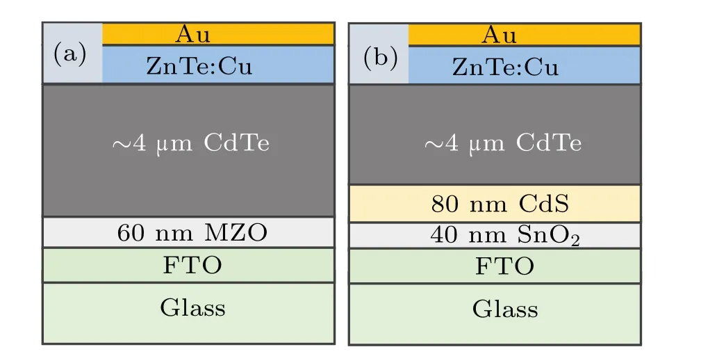
Fig.1. Schematic representation of CdTe solar cells used in this work: (a)FTO/MZO/CdTe and(b)FTO/SnO2/CdS/CdTe.
3. Results and discussion
3.1. Solar cell performance
The surface SEM images of CdTe deposited on MZO and CdS are given in Figs.2(a)and 2(c). The grain sizes(1 μm–2 μm)of polycrystalline CdTe deposited on CdS window layer are more uniform than on MZO,which range from a few hundred nanometers to several micrometers. This can be ascribed to the lack of O2in the CdTe deposition process. The O2can definitely affect the quality of CdTe film by tuning nucleation,grain size,pinhole formation,and defect chemistry.[19,21–23]
Figures 2(b)and 2(d)show the SEM cross-sectional microstructure of the window layer/CdTe junction region. The MZO layer is composed of densely-packed nanocrystals as shown in Fig.2(b). The nanocrystals indicate a large number of grain boundaries,which can increase recombination velocity at the p–n junction interface.[14,24]At the CdS/CdTe junction interface,the CdS film consists of mono grains.[25,26]And a thin CdSxTe1-xlayer is formed due to the interdiffusion between CdS and CdTe,which can reduce lattice mismatch and suppress interface recombination.The structural properties are significantly influenced by type and structure of the window layer, such as interface quality, preferential orientation, and grains size of CdTe.[27]And these properties will further affect the photovoltaic performance of cells.
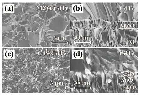
Fig.2. (a)SEM surface and(b)cross-sectional morphology at the interface of MZO/CdTe solar cell,(c)SEM surface,and(d)cross-sectional morphology at interface of CdS/CdTe solar cells.
The light and darkJ–Vcurves of the MZO/CdTe and CdS/CdTe solar cells with similar efficiencies are shown in Fig. 3(a). Detailed performance parameters are given in Table 1. Notably, neither of the cells shows “roll-over” or “Skink”phenomenon in theirJ–Vcurves. The lack of“S-kink”implies that CBO between the MZO and CdTe is not too high for solar cell devices.[16]TheVocof the MZO/CdTe solar cell is 805 mV,which is 42-mV higher than that of the CdS/CdTe cell. This is consistent with built-in voltage (Vbi) result obtained from thex-axis intercept of 1/C2–Vplots as shown in Fig.3(b). TheJscof MZO/CdTe solar cell is also a bit lower than that of the CdS/CdTe solar cell,which is counterintuitive as one should reduce optical loss and increaseJscby replacing CdS with MZO.[15]
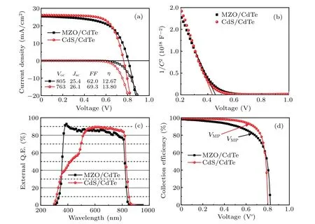
Fig.3. (a)Light(solid)and dark(hollow)J–V curves,(b)1/C2–V plots,(c)external quantum efficiencies(Q.E.),and(d)collection efficiency of the MZO/CdTe and CdS/CdTe solar cells,with VMP denoting optimum voltage.
Figure 3(c)shows the EQE curves of the two solar cells.The CdS/CdTe solar cell exhibits the typical optical loss in the short wavelength region(λ <510 nm)due to parasitic absorption of CdS window layer. As expected,this parasitic absorption is eliminated when CdS is replaced by MZO. However,for the MZO/CdTe devices,EQE loss occurs in the wavelength range of 600 nm–850 nm and this is responsible for failing to achieve highJscas expected. Generally,the reduced EQE response in this range is called deep-penetration loss,which results mainly from ineffective generation or insufficient carrier collection in bulk region or near back contact. The CdTe films of the devices in this study are all~4-μm thick,which is thick enough to absorb 99%photons with energy greater than band gap. Therefore,more significant losses in this range might result from more drastic bulk recombination in the CdTe film of MZO/CdTe solar cell than in CdS/CdTe solar cell. And this can be related to the lack of O2in the CdTe film deposition process of MZO/CdTe solar cell.
The current density (Jsc,EQE) integrated from the EQE data is 23.9 mA/cm2for the MZO/CdTe and 23.3 mA/cm2for the CdS/CdTe solar cell. TheJsc,EQEis lower than theJscat 1 sun, which results from the different setups for theJ–Vand spectral response measurements.[28]TheJsc,EQEof MZO/CdTe solar cell is higher than that of CdS/CdTe one,which is contrary to their correspondingJ–Vmeasurement results. There are two possible reasons for this phenomenon.Firstly, the EQE measurement is carried out in a range of 300 nm–900 nm, but the wavelength of light used in our solar simulator(Oriel Sol 3A)ranges from 400 nm to 1100 nm.The integrated current density calculated by the EQE data in the wavelength range of 300 nm–400 nm of the MZO/CdTe solar cell is~0.3 mA/cm2higher than that of CdS/CdTe solar cell. Secondary, both the CdS and CdTe exhibit photoconductivity under 1-sun illumination.[29]But for MZO, the photoconductivity usually occurs when wavelength of the incident light is lower than 400 nm.[30,31]The photoconductivity will increase the donor density in CdS and acceptor density in CdTe. The unchanged donor density in the MZO and increased acceptor density in the CdTe cause the depletion width to decrease. Consequently, the collection of carriers in the MZO/CdTe solar cell generated by the long wavelength light will decrease,while the collection of carriers generated by the long wavelength light will be less affected in the CdS/CdTe solar cell. Therefore,the difference in collection efficiency in the long wavelength range between the MZO/CdTe solar cell and CdS/CdTe solar cell will be lager under 1-sun illumination than under EQE measurement condition.
The PCE of the MZO/CdTe device is 12.67%,a bit lower than that of CdS/CdTe solar cell, 13.80%. The lower PCE is mainly caused by the lowerFF. TheFFis 62.0% for the MZO/CdTe and 69.3% for CdS/CdTe solar cell. TheFFdecreases with series resistance (RS,L) increasing and with shunt resistance (RP) decreasing. TheRS,LandRPare calculated from the line slope of the lightJ–Vcurves at the opencircuit voltage and short-circuit current points, respectively.As shown in Table 1, under 1-sun illumination theRS,Ldifference between the two solar cells is only 0.6 Ω·cm2. ButRPof the CdS/CdTe solar cell is about four times as great as that of the MZO/CdTe. This indicates more severe recombination in the MZO/CdTe solar cell than in the CdS/CdTe solar cell. Besides, theRpvalue of the CdTe solar cells is much larger under 532-nm monochromatic light illumination and/or infrared illumination(λ >850 nm)than under 1-sun illumination. According to our previous work,this phenomenon might result from the reduced incident light intensity and indicates that the shunting current is induced by the ohmic shunting path rather than the weak diode or space-charge limited current(SCLC).[32]
Table 1. The J–V parameters of CdTe solar cells.
3.2. Voltage-dependent collection efficiency
3.2.1. Under 1 sun
In order to ascertain the causes for poor performance of the MZO/CdTe solar cell, the voltage-dependent photocurrent collection efficiency,ηC(V′),is calculated. According to Hegedus,[33]theηC(V′)can be calculated from

whereJ1(V′)andJD(V′)are the output currents measured under illumination and in dark condition, respectively;JL01is the ideal photocurrent that can be approximated byJsc,or determined under reverse bias;Vis the applied voltage;V′represents theRS-corrected voltage. The actual voltage across absorption layer should be corrected toV′=V-RS×J(V),especially at high forward bias. In this work,RSis determined from the intercept of dV/dJ versus1/(J+Jsc)by using darkJ–Vdata,and is referred to asRS,D.[34]
Generally,collection loss of photocurrent occurs in these regions: space charge region(SCR),neutral region,and interfaces,and it is severely affected by carrier drift,diffusion and recombination.[33,35,36]For the CdTe absorber material, most of light is absorbed in SCR, where the electric field strength is high. Thus, the photo-generated carriers can be effectively separated by electric field when the applied voltage is low.As the applied forward bias increases, both the electric field strength and the width of SCR decrease. Reduction of the electric field strength leads the minority carriers to accumulate,and the carrier recombination to increase by defects at p–n junction interface. Meanwhile, the decrease of SCR width indicates that more light will be absorbed in neutral region.Without electric field, the photo-generated carriers cannot be separated effectively and then the bulk recombination will be enhanced. Figure 3(d) showsηC(V′) curves of the foregoing two cells under 1-sun illumination, which are calculated from Eq. (1). TheηC(V′) for each of the MZO/CdTe and CdS/CdTe solar cells is nearly 100%when the applied voltage is in a range of 0 V–0.2 V.For the applied voltage in a range of 0.2 V–0.7 V,theηC(V′)of MZO/CdTe solar cell is lower than that of CdS/CdTe solar cell. The greater collection loss in this region is related to more severe p–n junction interface and/or bulk recombination in MZO/CdTe solar cell. The photocurrent collection exhibits the lower loss in the MZO/CdTe solar cell when applied bias increases to aroundVoc. Because theVocandVbiin MZO/CdTe are a little higher than in CdS/CdTe solar cell.
Hegeduset al. reported that voltage-dependent photocurrentJL(V) reduces theFFof typical CdS/CdTe solar cell by 10%–15%,Vocby 20 mV–50 mV and efficiency by 2%–4%.[33]The decrement ofVocandFFcaused byJL(V) are calculated according to Eronet al.[37]and given below:
whereηC(Voc) andηC(VMP) are the collection efficiencies at forward bias ofVocand optimum voltage(VMP)at a maximum power (MP) point, respectively;A,k,T, andqare the ideal factor,Boltzmann constant,temperature,and electron charge,respectively.
The calculatedVocand FF loss caused byJL(V) of the CdS/CdTe solar cell under 1-sun illumination are 20.2 mV and 5.7%,respectively. And photocurrent loss at MP point is about 7.3%of theJsc. These results give an efficiency reduction of 1.53%.And the efficiency of this cell can increase from 13.80% to 15.33% after correcting forηC(V′). The losses in the MZO/CdTe solar cell are much higher, specifically, their values being 51.6 mV, 14.1%, 18.4%, and 3.89% for ΔVoc,ΔFF, photocurrent loss at MP point, and efficiency, respectively. The efficiency of this MZO/CdTe solar cell significantly increases from 12.67% to 16.56% after correcting forηC(V′). The more serious efficiency loss might result from the much more severe recombination in the MZO/CdTe solar cell.This is consistent withJ–Vresult that the MZO/CdTe solar cell has a lower shunt resistance.
3.2.2. Under 532-nm monochromatic illumination
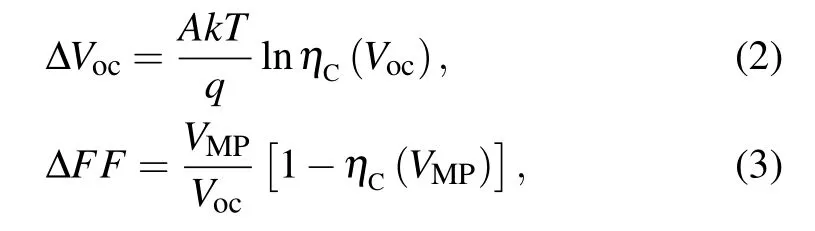
Figures 4(a)and 4(b)show theJ–Vcurves measured under 532-nm monochromatic illumination and the correspondingηC(V′)curves,respectively. The 532-nm monochromatic light will be absorbed within 100 nm from the layer/absorption layer interface due to high absorption coefficient of CdTe.[38]The carriers excited by 532-nm monochromatic light will be more seriously affected by p–n junction interface recombination. TheJ–Vcurves in Fig. 4(a) show that the MZO/CdTe solar cell has higherVoc,Jsc, and PCE than CdS/CdTe solar cell.While theηC(V′)of the MZO/CdTe cell is lower than that of CdS/CdTe cell when the applied forward bias is in a range of 0 V–0.7 V.This result suggests that there exists more serious p–n junction interface recombination in MZO/CdTe cells than in the CdS/CdTe cells, resulting in lower collection efficiency. TheηC(V′)of CdS/CdTe cell decreases very slowly when bias voltage is less thanVoc.This result indicates that the interface recombination between CdS and CdTe is quite weak.When the voltage is higher thanVoc,the electric field strength decreases to zero and the photo-generated carriers will accumulate in SCR and recombine by defects subsequently.
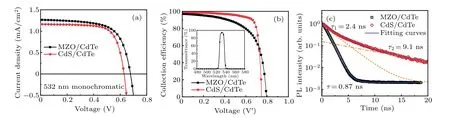
Fig.4. (a)The J–V curves and(b)collection efficiency of CdTe solar cells under 532-nm monochromatic illumination,with inset showing the transmission spectrum of the 532-nm monochromatic filter. (c)Time-resolved photoluminescence spectra of MZO/CdTe and CdS/CdTe solar cells.
The p–n junction interface recombination significantly affects the carrier lifetime in CdTe.Therefore,the TRPL is measured to compare the interface recombinations of the two solar cells. The incident light with a wavelength of 600 nm is excited from glass side and will be absorbed near the window layer/absorber interface. The TRPL spectra are shown in Fig.4(c). As can be seen,the CdS/CdTe solar cell exhibits the bi-exponential decay processes with two minority carrier lifetimes of 2.4 ns and 9.1 ns.The initial fast decayτ1is attributed to large recombination rate at the p–n junction interface.While the longer decayτ2represents the bulk recombination process in the CdTe film.[39]However,the MZO/CdTe solar cell shows only a much shorter carrier lifetime of 0.87 ns. These results prove that the MZO/CdTe solar cell exhibits more serious p–n junction interface recombination.
3.2.3. Under infrared illumination
The SCR width of a typical CdTe cell is in a range of 1 μm–2 μm, while the penetration depth in the CdTe film of light with a wavelength longer than 850 nm is more than 2 μm.Minority carriers excited by this infrared light are generated near the back contact and have to diffuse from neutral region to SCR before being collected. However, diffusion length is much shorter than drift length in the CdTe.[35]Therefore,carriers excited by infrared light are more likely to be recombined by defects located in CdTe bulk before arriving at p–n junction interface. Figures 5(a)and 5(b)show theJ–Vcurves andηC(V′)of the two solar cells under infrared illumination.Although the MZO/CdTe solar cell has higherVocthan the CdS/CdTe solar cell, itsηC(V′) is much lower in a range of 0 V–0.65 V. The lowerηC(V′) implies more severe bulk recombination in the MZO/CdTe solar cell than the CdS/CdTe solar cell.
Impedance spectroscopy is a useful tool to investigate carrier recombination at hetero-junction structural interface in solar cell device. In order to study the recombination around CdTe/ZnTe:Cu interface, the impedance spectroscopy is performed. In the measurements,the MZO/CdTe and CdS/CdTe solar cells are biased in the dark under a positive potential of 0.5 V and the applied frequency ranges from 50 Hz to 200 kHz. Figure 5(c) shows the Nyquist plots of the MZO/CdTe and CdS/CdTe solar cells. The inset in Fig. 5(c)shows the equivalent electronic circuit employed to fit the impedance spectra. The equivalent electronic circuit includes a series resistanceRS, a recombination resistanceRrec, and a capacitor. As shown in Fig. 5(c), the data can be well fitted with the equivalent electronic circuit. The obtained series resistances for the two solar cells are almost the same.The recombination resistanceRrecvalue is 228 Ω·cm2for the MZO/CdTe and 1079 Ω·cm2for the CdS/CdTe solar cell.When the applied forward bias is high, the recombination resistanceRrecrepresents the recombination near the back contact . Therefore, the MZO/CdTe solar cell suffers more serious recombination near the back contact interface than the CdS/CdTe solar cell. And the serious recombination near the back contact is responsible for the low EQE values of MZO/CdTe solar cell in the range of 600 nm–850 nm as shown in Fig.3(c).This is consistent with the photocurrent collection efficiencies of the two solar cells under infrared illumination.
Fig. 5. For MZO/CdTe and CdS/CdTe solar cells, (a) J–V curve, (b) curve of collection efficiency versus voltage under infrared illumination, with inset showing the transmission spectra of the infrared filter,and(c)curve of Nyquist plots,with inset showing equivalent electronic circuit model employed to fit the experimental spectrum data.
3.3. Collection loss mechanism
The collection efficiency losses under 532-nm monochromic and infrared illumination indicate more serious recombination both at p–n junction interface and in bulk CdTe near the back contact in the MZO/CdTe solar cell than in the CdS/CdTe solar cell. In order to ascertain which mechanism is dominant in each solar cell, theJ–V–Tcharacteristics are carried out. TheJ–Vcurves of the MZO/CdTe and CdS/CdTe solar cells, are measured at different temperatures and shown in Fig.6. None of these curves exhibits“S-kink”phenomenon over the temperature range we tested. The “roll-over” exists at low temperature(T ≤250 K)and results from non-Ohmic back contact. The activation energyEaof reverse saturation current is obtained by the model that Turcuet al.reported.[40]TheJscis a function ofVocexpressed as follows:whereJ0is the reverse saturation current density, andJ00is related to carrier mobility and defect concentration. Thus,Voccan be expressed by,IfA,Jsc, andJ00are temperature-independent, a plot ofVocversus Tyields a straight line. By extrapolating this line toT= 0 K, the activation energyEawill be obtained. This method has been widely used to determine the activation energy of CdS/CdTe solar cells.[34,41,42]IfEais smaller thanEgof the absorber material of a solar cell, the recombination is dominant at p–n junction interface. IfEais similar toEgof the absorption layer, the recombination is dominant in bulk region.[43]The curves ofVocas a function of temperature(T)for the MZO/CdTe and CdS/CdTe solar cells are plotted in Fig.7. TheEavalues obtained are 1.08 eV and 1.36 eV for the MZO/CdTe and CdS/CdTe solar cells,respectively,indicating that recombination mechanism of the CdS/CdTe solar cell is mainly controlled by Shockley–Read–Hall(SRH)recombination in the bulk region.[43]TheEavalue of the MZO/CdTe solar cell is much lower than 1.45 eV, which implies that the interface recombination is the dominant mechanism in this device.

Fig.6.The J–V curves of(a)MZO/CdTe solar cells and(b)CdS/CdTe solar cells at different temperatures.

Fig.7. The Voc as a function of temperature(T)of(a)MZO/CdTe solar cell and(b)CdS/CdTe solar cell.
The tunneling-enhanced interface recombinations widely exist in Cu(In,Ga)Se2, CuGaSe2, CdTe, and Cu2ZnSnS4thin film solar cells.[44–47]A quantitative analysis was introduced to describe the tunneling at the junction in a Schottky barrier.[48,49]Rauet al.extended this model to describe the diode current from pure SRH recombination to tunneling-enhanced interface recombination.[50]In the Padovani–Stratton model,the ideal factor can be described by
whereE00is characteristic tunneling energy and related to the tunneling probability. The contribution of tunneling increases withE00increasing andTdecreasing. WhenE00is close tokT,the tunneling-enhanced recombination is dominant,while whenE00≪kT,pure thermionic emission is dominant.[49,51]In the CdTe solar cell, the thermionic emission refers to the pure SRH recombination.

Fig.8.Plots of ideal factor A versus temperature T for MZO/CdTe solar cell and CdS/CdTe solar cell,in a temperature range of(a)80 K–320 K,and(b)230 K–320 K.
The ideal factors of the MZO/CdTe and CdS/CdTe solar cells together with fitting curves to Eq. (6) are shown in Fig. 8(a). From these fits the obtained characteristic tunneling energyE00is 55 meV for the MZO/CdTe and 45 meV for CdS/CdTe solar cells. For CdS/CdTe solar cell, equation (6) is not applicable around room temperature as shown in Fig. 8(b). It is believed that tunneling-enhanced interface recombination dominates the reverse saturation current of a CdS/CdTe solar cell only when the temperature is approximately below 240 K.[45,46]For the MZO/CdTe solar cell,tunneling-enhanced interface recombination is involved over the entire temperature range(80 K≤T ≤320 K)we tested. In our previous work,the electron concentration of MZO film after being annealed is about 1018cm-3,[13]which is higher than that in CdS film. Therefore,tunneling is more likely to occur in the MZO/CdTe devices.
3.4. SCAPS simulation
Capacitance–frequency(C–f)response can be used to determine the defect concentration in CdTe absorber.[52,53]Figure 9(a) shows the density of defect states calculated by using a model proposed by Walteret al. withC–fdata.[54]The peak at the energy of 0.44 eV–0.45 eV is corresponding to the VCd, or TeCdor (TeCd+2VCd)2-defect complex.[55,56]Total defect concentration(Nt)is obtained by integrating the defect distribution curve. The estimated defect concentration of the MZO/CdTe and CdS/CdTe solar cells are 4.53×1013cm-3and 5.15×1012cm-3, respectively. It is reported that the mid-gap defect (about 0.75 eV above the VBM) in the CdTe film plays the main role in degrading cell performance,which is thought to be associated with a complex of V2-Cdand an impurity.[57–59]But it is beyond ourC–ftesting range. Therefore,SCAPS simulation is carried out to study the influence of interface and bulk SRH recombination on CdTe solar cell performance. Detailed parameters used in simulation are listed in Table 2.[10,13,59,60]

Fig. 9. For MZO/CdTe solar cell and CdS/CdTe solar cell, (a) defect density of state versus Et–Ev, simulation J–V curve for different (b)concentrations of defects at(b)Et1–Ev=0.45,(c)Et2–Ev=0.75 eV,and(d)for interface recombination velocities(S)between CdS and CdTe.
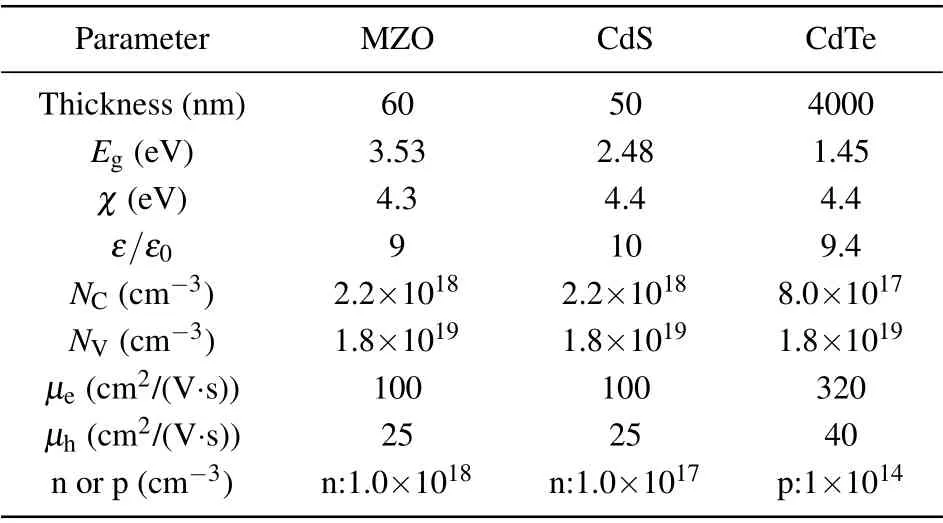
Table 2. Parameters used for SCAPS simulations.
In this one-dimensional simulation, the back contact is assumed to be Ohmic. Figures 9(b)–9(d) show the simulatedJ–Vcurves of a CdS/CdTe solar cell with different values of defect concentration(Nt)of a hole trap,Et1,located at 0.45 eV above valence band maximum (VBM), mid-gap defect level,Et2,and interface recombination velocity(S)between the CdS and CdTe, respectively. BothEt1andEt2existed in the bulk CdTe film. As shown in Figs. 9(b) and 9(c), when the concentrations of the two defects are both lower than 1014cm-3,theJ–Vcurves of the cell with different defect concentrations are almost overlapped. When the concentration is higher than 1014cm-3, the performance of the cell will significantly degrade with the increase of defect concentration,especially for the mid-gap defectEt2. According to theC–fmeasurements,the obtainedEt1concentration in the MZO/CdTe solar cell and CdS/CdTe solar cell are both lower than 1014cm-3. Thus,the defectEt2should be responsible for the difference in bulk recombination for CdTe. The device performance shows the strong correlation with the interface recombination velocity(S) between CdS and CdTe as shown in Fig. 9(d). TheVocof the cell drastically decreases withSincreasing. TheJscandFFare influenced by interface recombination only whenSis higher than 104cm/s.
ThenJ–Vperformance of the MZO/CdTe and CdS/CdTe solar cells shown in Fig. 3(a) are simulated. In the simulation, the concentration ofEt1is determined by theC–fmeasurements. And the influence of concentration of defectEt2and interface recombination velocity are taken into consideration. The simulated curves together with the experimental data are displayed in Fig. 10. From the simulation, the obtained interface recombination velocity of the MZO/CdTe and CdS/CdTe solar cells are 2×106cm/s and 2.4×104cm/s, respectively. This result is consistent with the conclusion derived from TRPL measurements. And the concentration of defectEt2obtained are 2×1014cm-3and 4×1013cm-3for the MZO/CdTe solar cell and CdS/CdTe solar cell, respectively.And this can explain the more severe photocurrent collection loss in MZO/CdTe solar cell under infrared illumination.

Fig.10.Experimental J–V data and simulated J–V curves of(a)MZO/CdTe and(b)CdS/CdTe solar cells.
According to the above discussion, the band diagram of MZO/CdTe heterojunction and CdS/CdTe heterojunction under equilibrium state at room temperature are depicted and shown in Figs.11(a)and 11(b),respectively.We conclude that the bulk SRH recombination in CdTe was dominated in the CdS/CdTe solar cell and the interface recombination is dominated in the MZO/CdTe solar cell. And tunneling enhanced interface recombination is also involved in the MZO/CdTe solar cell at room temperature. The bulk SRH recombination,p–n junction interface recombination,and tunneling-enhanced interface recombination are marked by path 1, path 2, and path 3 in these figures, respectively. And the dominated current mechanism in each solar cell is emphasized by bold arrows.

Fig. 11. Band diagram of (a) MZO/CdTe and (b) CdS/CdTe heterojunctions. EC, EV, and EF are the conduction-band-edge, valence-band-edge,and Fermi-level. Paths 1, 2, and 3 are three possible recombination pathways through defects at room temperature, namely, bulk Shockley–Read–Hall recombination,interface recombination,and tunneling-enhanced interface recombination, respectively. The dominant recombination process in each junction is marked by bold arrow.
4. Conclusions
In this work, a comparative study is performed between the MZO/CdTe and CdS/CdTe solar cells with similar performances. It was found that more serious performance loss existed in the MZO/CdTe solar cell than that in the CdS/CdTe solar cell. And this is induced by more severe recombination at the p–n junction interface and in the CdTe bulk region near the back contact. The activation energy is 1.08 eV for the MZO/CdTe solar cell and 1.36 eV for CdS/CdTe solar cell, respectively. This suggests that the bulk SRH recombination in CdTe is dominated in the CdS/CdTe solar cell,while the p–n junction interface recombination is dominated in the MZO/CdTe solar cell. In addition, we also find that the tunneling enhanced interface recombination mechanism is involved in the MZO/CdTe solar cells at room temperature.Moreover, the results of SCAPS simulation support the conclusion that the MZO/CdTe solar cell has a higher interface recombination velocity and bulk defect concentration than the CdS/CdTe solar cell. This work indicates that for poor performance MZO/CdTe solar cell, more efforts should be made to suppress the recombinations both at the p–n junction interface and in bulk CdTe.
Acknowledgement
Project supported by the National Natural Science Foundation of China(Grant Nos.61774140 and 61474103).
猜你喜欢
海峡姐妹(2021年2期)2021-03-07
科学导报(2020年24期)2020-04-24
音乐生活(2019年12期)2019-10-10
科学导报(2019年48期)2019-09-25
科学导报(2018年36期)2018-05-14
红领巾·探索(2016年10期)2016-12-07
- Chinese Physics B的其它文章
- Formation of high-density cold molecules via electromagnetic trap
- Dynamics of molecular alignment steered by a few-cycle terahertz laser pulse
- Terahertz spectroscopy and lattice vibrational analysis of pararealgar and orpiment
- Molecule opacity study on low-lying states of CS
- Finite-time Mittag–Leffler synchronization of fractional-order complex-valued memristive neural networks with time delay
- Ultrafast Coulomb explosion imaging of molecules and molecular clusters